

AN1126
V
®
APPLICATION NOTE
CURRENT SHARING OF THE L4973
IN A MULTIPHASE APPLICATION
by Domenico Arrigo & Giuseppe Gattavari
INTRODUCTION
The L4973 family is a 3.5A monolithic s tep-down dc-dc converter, available in POWERDIP18( 12+3+3)
and SO20L (12+4+4) plastic packages. The operating input supply voltage range is f rom 8V to 55V, and
the output ranges from 3.3V (L4973D3.3) and 5.1V(L4973D5.1) to 40V. Other regulated outputs below
3.3V are also possible (See Application Note AN938).
Using two L4973D is possible to deliver up to 7A with a good sharing between the two sections or a re-
dundant 3.5A. The two devices work at a switching frequency of 200kHz. At Vcc = 24V, V o = 5.1V at 7A
the efficiency is 87%. At 3.5A output, the efficiency is 90%.
Electrical Specifications
Input Voltage range 8V-30V
Output Voltage 5.1V ±3% (Line, Load and Temperature)
Output Voltage Ripple 47mV (0.92%/Vo)
Output Current range 0 to 7A
Max Output Ripple current 15%
Min Iomax Current limit 8A
Switching frequency 200kHz
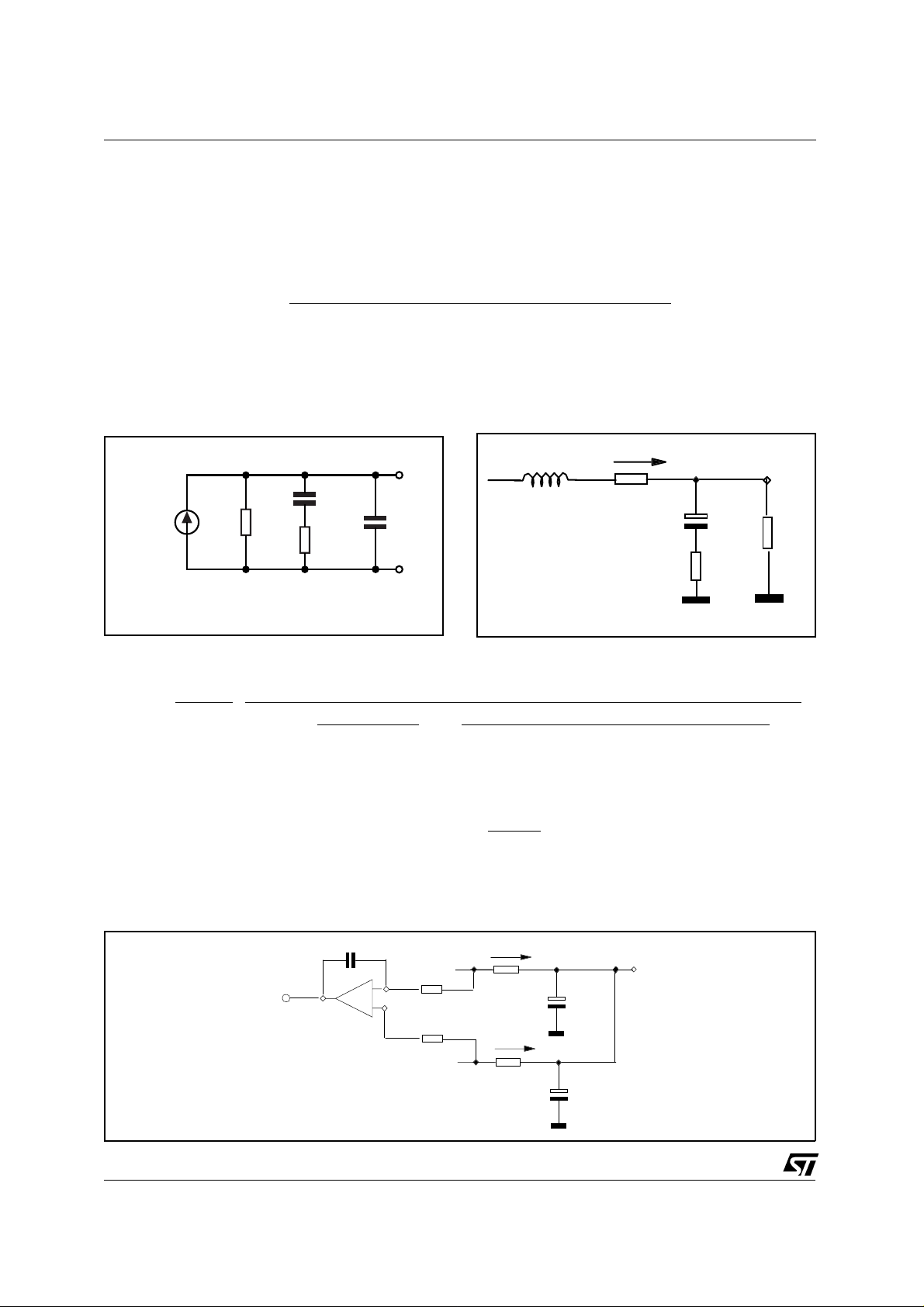
Current Sharing Operating Principle
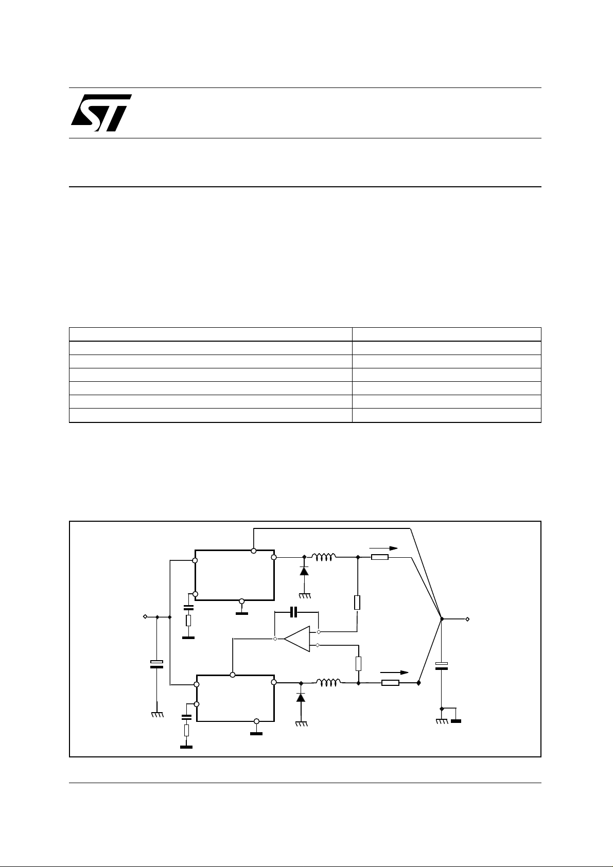
The current sharing configuration, shown in fig. 1, is based upon two L497x devices U1 and U2. Any device in the L497x family can be used for this purpose.
The U1 regulator acts as a master which regulates the output voltage.
The second section U2 works as a current follower. Its task is to deliver an output current equal to the
Figure 1. Current Sharing Operating Princi ple
Rint
I -FB
Rs
Vout
I +
Rs
Cout
Vcc
U1
COMP
cc
Vcc
COMP
L497x
FB
U2
L497x
GND
OUT
Cint
OP-AMP
OUT
GND
L
+
L
May 1999
1/16
AN1126 APPLICATION NOTE
current delivered from the first section. An op-amp compares the voltage drop through Rs which is proportional to the cur rent deliv er ed from the U2 section with the voltage drop across Rs proportional to the
current delivered from the U1 section. T he Cin and Rin components introduce a pole and a zero in the
current loop which allows integration of the error signal. The current loop regulates I
result the output current delivered to the load is Iout = 2I- = 2I+ for every load condition.
Current Sharing Accuracy
The accuracy of the current sharing between the two sections depends on the op-amp offset voltage,
Voff, and the value of Rs and its ac curacy . The of fset voltage introduce an error in the sensing voltage ,
Vs=Rs Iout/2 . The relative percentage current error due to the offset is given by :
e%= (∆ I/I) ⋅ 100 = (Voffset ⋅ 100) / (Rs ⋅ Iout)
This error is minimum at maximum load. The larger the value of Rs, the smaller the error. Rs must be
chosen as a compromise between error minimization and system efficiency.
For example with Iout = 7A choosing Rs = 25mΩ ,considering a maximum offset voltage of 3mV
(LM358A), the maximum relative percentage error is 1.7% (120mA @ Iout = 7A).
The total error is given by the sum of this error plus the error due to the sensing resistor ( which corresponds to its accuracy of 1% ). So the maximum error is 2.7% (190mA @Iout = 7A)
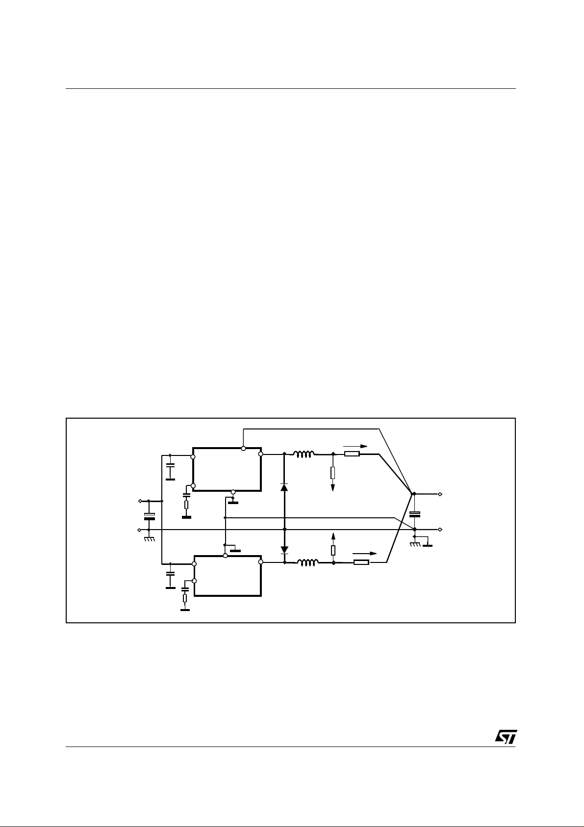
Layout Hints
The PCB layout requires some care. The power paths of the two sections must be as short and symmetrical as possible. The current sensing wires must be parallel and s hort to avoid induced noises. The
sensing resistor must be non induct ive. The ground pins of the two devices must be at the same voltage
and connected to the output ground point.
Figure 2. Layout hints.
+
equal to I- . As a
to the
current
FB
I -FB
Rs
to the
current
FB
Vout
Cout
GND
I +
Rs
Vcc
GND
COMP
Vcc
Vcc
COMP
U1
L497x
U2
L497x
L
OUT
GND
GND
L
OUT
Syncronization or Multiphase
In a current sharing application the two sections c an be synchronized. This permits a reduction of noise
induced from one section to another. In this case a single RC network can be used for both the oscillators and the two SYNC pins are connected.
In many application, instead of synchronizing the two oscillator, it is useful to introduce a delay between
the two PWM signals in order to achieve a multiphase application. The phase shift between the two
PWM signals can be easily achieved by two methods :
2/16
AN1126 APPLICATION NOTE
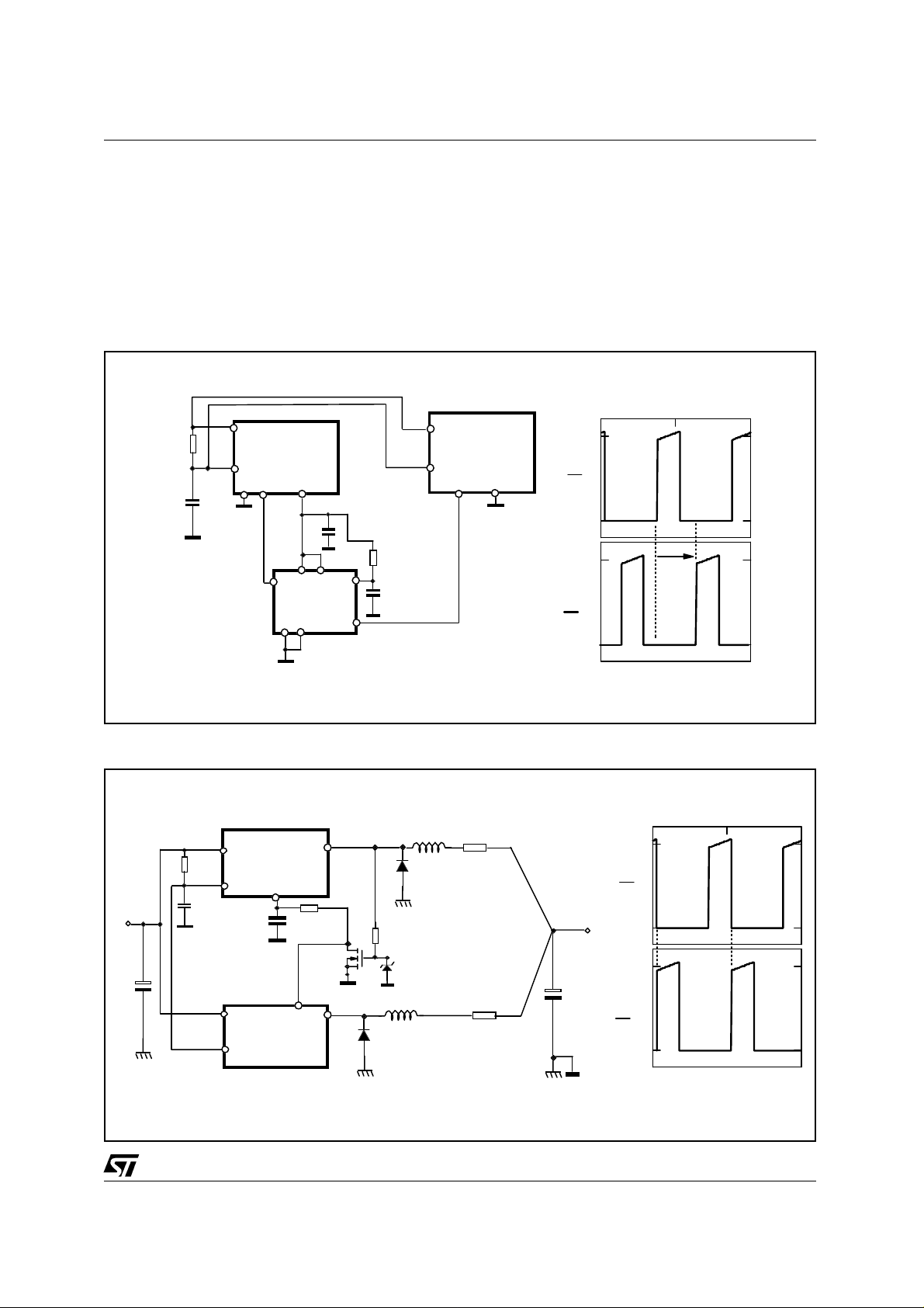
Case 1)
Programmable Phase Delay.
Fig. 3 shows how to program a phase delay with a monostable multivibrator whos e on time is equal to
the desired phase delay.
Case 2)
Fixed Phase Delay.
Figure 3 shows a method of setting a delay time for the 2nd PWM section to be slightly larger than the
ON-time of the 1st PWM section.
Figure 3. Case 1) Programmable Phase Delay.
Vcc
R1
OSC
GND
U1
L4973D3.3
SYNC
Vcc
1B
M74HC123
1A
GND
Vref=5.1C2
CLR
_
1Q
Vcc
OSC
U2
L4973D3.3
SYNC
U1
GND
U2
PWM OUTPUTS
0
α
0
Figure 4. Case 2) Programmable Phase Delay.
L
18V
*
L
Vcc
necessary if Vcc>18V
*
OUT1
OUT2
Vcc
R1
OSC
C2
Vcc
OSC
U1
L4973D3.3
Vref=5.1
SYNC
U2
L4973D3.3
t
PWM OUTPUTS
Rs
Vout
Cout
Rs
U1
0
U2
0
t
3/16
AN1126 APPLICATION NOTE
Multiphase Benefits
The main benefits are :
Minimization of the RMS current through the input capacitor therefore increasing of the efficiency and
reducing of the capacitor cost and size.
Minimization of ripple current through the output capacitor and ground path.
Fast load transient response.
Improved reliability /MTBF.
RMS current through the input capacitor are equivalent in Case 1) and Case 2). Even though the circuitry of Case 2) is simplifier than Case 1), Case 1) provides the opportunity to optimize this ripple current.
Minimization of the RMS Current Through the Input Capacitor.
In Case 1) , Figure 3 shows the RMS current through the input capacitor, referred to the output current
(Iout), for various phase delays, α , of the two PWM sections. This assumes a duty cycle of 0.5 and a
ripple current through the coil of 0.1⋅ Iout.
For α equal to a half period (180 degrees of phase delay) the RMS current is approximately zero. If the
two PWM signals are synchronized the RMS value is Irms = Iout/2. For example if Vout = 5V and
Iout = 7A the Output Power is 35W. If the Input capacitor has an ESR of 100mOhm the phase delay
allows a savings of 1.23W which corresponds to the 3.5% of the power delivered to the load.
Figure 5. RMS current through the input capacitor for a different phase delay, α , with a duty
cycle of 0.5.
[ A ]
α=120
°
Iout/2
0
- Iout/2
α=40
0
Assuming the same duty cycle for the two sections, the RMS Current through the input filter for different
duty cycle, considering a phase delay of the second PWM signal equal to the Ton of the first section (
Case 2) ), is given approximately (the output c urrent ripple can be negleted for this calculation) by the
following formula:
2
− (Iout ⋅
I
RMS
(α)
Iout
√
=
⋅
√2 ⋅ δ
2
Iout
√
where δ = duty cycle
2
(3
⋅
2
⋅ δ −1)
√
⋅
α=180
°
δ
2
− (iout ⋅
2
)
°
if
δ)
α=90
°
α=0
time
0.5
δ ≤
2
if δ > 0.5
°
Multiphase (1)
4/16
AN1126 APPLICATION NOTE
Iout is the total output current equal to the sum of the individual output currents delivered from the two
sections.
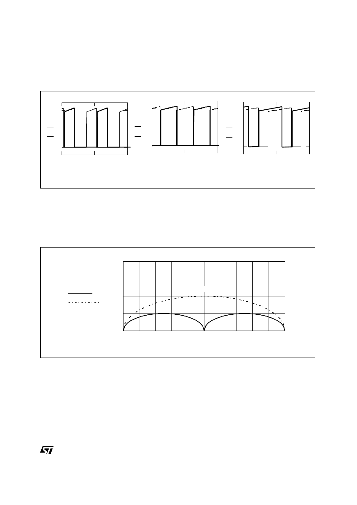
Figure 6. Input current of the two sections for different dut y cycle.
PWM1
PWM2
PWM1
PWM2
1
0
0
t
δ=0.5
1
0
0
t
δ<0.5
1
PWM1
PWM2
0
0
t
δ>0.5
If the PWM signals are synchronized without any delay, the RMS current through the input filter as a
function of duty cycle is :
Irmssync
(Iout
(δ) =
√
⋅ √δ )
2
− (Iout ⋅
2
synchronized (2)
δ)
Figure 7. RMS current through the input capacitor with synchronizat ion and with multiphase.
Iout
[ A ]
3Iout/4
δ
Irms ( )
Irmssync ( )
δ
Iout/2
Irms
Iout/4
Irmssync
0
0 0.1 0.2 0.3 0 .4 0.5 0.6 0.7 0.8 0.9 1
δ
Figure 7 shows Equations (1) and (2) versus the duty cycle.
The maximum RMS current with synchronized PWMs is 1/2 of the total output current and it is obtained
for δ = 0.5.
In contrast, considering the multiphase PWM,
RMS value is 1/4 of the total output current.
the RMS value is 0 with δ = 0.5
So the maximum RMS current with multiphased PWMs
and the max value of the
is a half of that syncronized PWMs.
For every duty cycle condition the RMS current with multiphase application is lower than the case with
synchronized PWMs and it is quite regular for different duty cycles.
It allows to optimize the input capacitor for the real working condition. In the synchronized case the input
capacitor has to be dimensioned f or the worst case of δ = 0.5 that can be far from the real working conditions.
5/16
AN1126 APPLICATION NOTE
If Psync is the wasted power on the input capacitor with synchronized PWMs, given by :
Psync = ESR ⋅ Irmssync
2
and Pmulti is the wasted power with multiphased PWMs, given by :
Pmulti = ESR ⋅ Irms
2
the power saved using the multiphase instead of the synchronized method for various duty cycle is :
Psaved (δ) = ESR ⋅ (Irmssyn c
ESR
Psaved
(δ) =
ESR
I
⋅
out
2
⋅ I
out
2
2
2 ⋅
⋅
2
(δ) - Irms2 (δ))
δ if
1
if δ >
δ)
(
−
δ
≤
0.5
0.5
For example considering an input capacitor ESR of 0.1 Ohm and an output current of 7A the power
saved using the multiphase instead of the synchronized method for different duty cycle is shown in fig.8.
Figure 8. Power saved using the multiphase instead of the synchronized method for various
duty cycle.
2
[W]
1.5
1
Psaved (δ)
Psync
Pmulti
(δ)
(δ)
Psync
0.5
0
0 0.1 0.2 0.3 0.4 0.5 0.6 0.7 0.8 0.9 1
Figure 9. Power saved vs. Vout
[W]
2
Vin=12V
Ω
Iout=10A
Iout=7A
Vout [ V ]
6/16
Psaved
ESR=60m
1.5
1
0.5
0
3 3.5 4 4.5 5 5.5 6 6.5 7 7.5 8
Iout=5A
Psaved
Pmulti
δ
[W]
Psaved
2
Vin=12V
Iout=7A
1.5
1
0.5
0
33.544.555.566.577.58
ESR=100m
Vo u t [ V ]
Ω
ESR=75m
ESR=50m
Ω
Ω

Figure 10. Power saved vs. Iout.
AN1126 APPLICATION NOTE
Psaved
[ W ]
Psave( ),,,Iout 5.1 12 0.05
Psave( ),,,Iout 5.1 12 0.085
Psave( ),,,Iout 5.1 12 0.1
2
Vcc=12V
Vo=5.1V
1.5
fsw=200kHz
1
0.5
0
0 1 2 3 4 5 6 7 8 9 10
ESR=100m
Iout
[ A ]
Ω
85m
50m
Ω
Ω
The gained power as a percentage of the output power using the multiphase PWMs instead of synchronized PWMs is :
∆P%(δ) =
∆P%(δ) =
Psaved
ESR
(δ)
⋅ 100
Po
Iout
⋅ 100
⋅
2
Vcc
So the percentage gained power, ∆P%, for a fixed Iout, Vcc and ESR does not change with the output
voltage.
For example if the input capacitor has an ESR of 100mOhm for a 12V/3.3V or 12V/5V power conversion,
with Iout = 7A, there is in both cases a ∆P% gain of 3% .
Table1 shows in details the major tips for different output voltages.
Table 1. Vcc = 12V , Iout = 7A, ESR=100mΩ.
Vo
(V)
3.3 3.13 1.74 1.39 0.98 0.3 0.68 3%
5.1 3.46 1.25 2.21 1.2 0.16 1.04 3%
6 3.5 0 3.5 1.23 0 1.23 3%
Irmssync
(A)
Irmsmulti
(A)
Irms
∆
(A)
Psync
(W)
Pmulti
(W)
Psaved
(W)
P%
∆
Gained
The gained power ∆P% versus duty cycle is shown in figure 10.
7/16

]
AN1126 APPLICATION NOTE
Figure 11. ∆P% vs. duty cycle.
6
5
4
∆
P%(δ)
3
2
1
0
0 0.1 0.2 0.3 0.4 0.5 0.6 0.7 0.8 0.9 1
Figure 12. ∆P%
∆
P%=(Psaved/Po) · 100
∆
P%
6
ESR=60m
5
4
3
2
1
Ω
Vcc=8V
δ
Vcc=12V
Vcc=24V
∆
P%
10
8
6
4
2
The gained power ∆P% as a function
of input voltage, output voltage, output
current and input capacitor ESR is
shown in figure 12.
Figure 12 shows the measured efficiency with the L4973D board , with
Vin = 12V, Vout = 5.1V, fsw = 200kHz,
using a input capacitor 470µF/50V
ROE with an ESR = 85mΩ. Using the
multiphase application with a phase
delay, α, equal to half period, case1) ,
there is a gained efficiency of 2%
compared to the synchronous application. So it is possible to maintain high
efficiency values using low cost and
size capacitor.
∆
P%=(Psaved/Po) · 100
Vcc=12V
ESR=100m
Ω
50m
75m
Ω
Ω
0
02468101214161820
Iout [ A ]
Figure 13. Efficiency vs. Output Current.
V
⋅ I
O
VIN ⋅ I
O
⋅ 100
IN
η
=
[%]
95
Cin = 470µF/50V ROE EKE
ESR = 85 m Ohm
Multiphase
α=180
90
synchronous
85
Vcc = 12V
Vo = 5.1V
fsw = 200kHz
80
012345678
Io [A
02 4 6 8 101214161820
Iout [ A ]
Conclusions
To sum up in application in which the duty
cycle is between 0.2 and 0.8 t here is a big
advantage using the multiphase PWMs, in
terms of dissipated power on the input capacitor compared with the added circuitry to
achieve it. The more the output current is
the more this advantage increases.
Applications with δ = 0.5, using a half period
of multiphase phase delay, gives the best
benefit because the RMS current through
the input capacitor is approximately zero.
Minimization of the Ripple Current
Through the Output Capac itor.
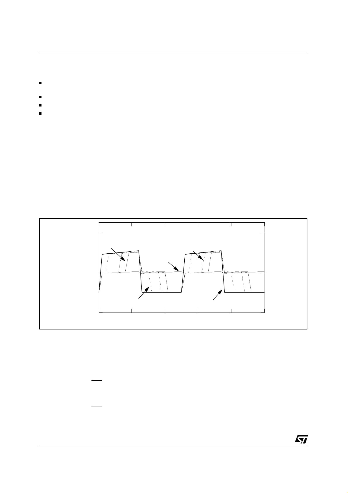
Figure 13 shows the current ripple through
the output filter for different phase delay, α,
of the two PWMs considering a duty cycle of
0.5.
8/16

AN1126 APPLICATION NOTE
For α equal to half period (180 degrees
Figure 14. Ripple current through the output
of phase delay) the ripple current is approximately zero.
This allows to chose low cost output filtering
capacitor. Or, with the same ESR, to reduce drastically the output voltage ripple.
The phase shift between the two PWM signals can be easily achieved in two way.
If the duty cycle is far from 0.5, the ripple
current through the output capacitor is
higher in Case 2 than in Case 1 in which
the delay time can be programmed.
−∆Ιο/2
Current Sharing Evaluation Board for L4973D
Figure 15. Current sharing schematic diagram.
+∆Ιο/2
capacitor for different phase delay, α.
α=40
α=0
α=90
°
°
α=180
0
α=120
°
0
°
°
t
α=240
°
Vcc (8V to 30V)
C1
680uF
35V
C3
680uF
35V
C7
220nF
220nF
C17
C2
1.2nF
J2
INH1
Vcc
22k
R1
OSC
OSC
Vcc
INH2
J3
1uF
C20
INH
V5.1
8,9
1111
19
SS
15nF
SYNC
1
8,9
11
18
FB
INH
11
U1
L4973D
20
SYNC
C5
20
U2
L4973D
19
SS
13
V5.1
C10
1uF
1/2
LM358
SO8
FB
13
4,..,7
14,..,17
C15
15nF
BOOT
18
Vcc
4,..,7
14,..,17
7
R7*
BOOT
COMPGND
C16
4.7nF
R8
10K
GND
Z1*
220nF
C6
10
OUT
2,3
12
COMP
C4
22nF
R2
10K
C14
Cin=10nF
4
+
8
C13
100nF
220nF
C18
10
2,3
OUT
D2
STPS
640CB
12
C19
220pF
D1
STPS
640CB
6
5
C9
220pF
R11
Rin=10K
10K
L1 43uH
(77120) N=34
R5
L2 43uH
(77120) N=34
25m
R6
25m
C12
220nF
Iout=7A
Ω
R3
C8
220uF
R4
Ω
R9
C21
220uF
C23
220nF
* Z1 and R1 are necessary only if Vcc>25V
9/16

AN1126 APPLICATION NOTE
Electrical Specifications and Performance:
Input Voltage range 8V-30V
Output Voltage 5.1V ±3% (Line, Load and Temperature)
Output Voltage Ripple 47mV (0.92%/Vo)
Output Current range 0 to 7A
Max Output Ripple current 15%
Min Iomax Current limit 8A
Switching frequency 200kHz
Efficiency 87% @ 7A Vin = 24V
Figure 16. Board efficiency vs. output current.
η
[%]
95
Vcc=8V
10V
12V
90
15V
20V
85
24V
Table 2. Output voltage selection
L4973D3.3
Vo (V) R3 (KΩ)R4 (K
3.3 0 4.7
5.1 2.7 4.7
L4973D5.1
5.1 0 4.7
)
Ω
80
Main Components Description.
Vo=5.1V
75
fsw=200kHz
It follows a description of the chosen output and input capacitor and of the i nductor for each of the two sections.
70
012345678
Io [A ]
Input Capacitors
The input capacitors have t o be able to support the maximum input operating voltage of the device and
the maximum RMS input current.
At full load, Io = 7A and duty cycle of 50% the RMS current flowing through the input capacitors is
maximum and is given by Io/2 . So the RMS current to be sustained is 3.5A.
The two selected capacitor, FA 680µF/50V Panasonic, are able to support this current.
Inductor Selection
The minimum duty cycle is:
Dmin = (Vo + Vf )/(Vin max + Vf )= 0.184
where Vf is the freewheeling diode forward voltage.
The inductor ripple current is fixed at 15% of Iomax and it is 0.525A.
The inductor needed for each of the two sections is:
The L ⋅ Io
Vo
(
L =
2
is 0.533 and the size cor e chose is 77120 (125µ) Magnetics KoolMµ material. In order t o
+ Vf
1 – D
⋅ (
)
f
I
⋅
∆
o
sw
min
)
= 43µH
compensate a 40% reduction of in ductance at full load due to t he DC current level, it is necessary to
wire 34 turns, which correspond to 84µH of inductance at light load.
10/16

AN1126 APPLICATION NOTE
With this choice the core losses are approximately 280mW. The temperature increasing of the core is
12°C approximately.
Output Capacitor
The selection of Cout is driven by the output ripple voltage required, 1% of Vo. This is defined by the
ESR of the output capacitance and by the maximum ripple current (0.525A).
The maximum ESR is:
ESR = ∆Vo/∆Io = 0.051/0.525 = 97m
Ω
The selected capacitance is 220µF/35V FA Panasonic with ESR = 90mW and the ripple voltage is
0.92% of Vo (47mV).
Bill of Material
C1, C3 680µF / 35V FA PANASONIC 16x15 Irms=1690mA
C2 1.2nF/35V SMD 1206
C4 22nF SMD 1206
C16 4.7nF SMD 1206
C13 100nF/35V SMD 1206
C5,C15 15nF/35V SMD 1206
C6,C7,C12,C17,C18,C23 220nF/50V SMD 10% Kemet 1206 X7R
C8,C21 220µF/35V FA PANASONIC 8x15
C10,C20 1µF/10V electrolitic (not SMD)
C11,C22 not used
C14 10nF/35V SMD 1206
C9,C19 220pF SMD 1206
U1,U2 L4973D3.3
R1 22k SMD 1% 1206, 0.25W
R2 9.1k SMD 1% 1206, 0.25W
R3,R10 2.7k SMD 1% 1206, 0.25W
R4,R12 4.7k SMD 1% 1206, 0.25W
R6,R9 0.025 Ohm 1W 1% DALE WSL-2512
R7 0 SMD 1206
R11,R5,R8 10K SMD 1% 1206, 0.25W
D1 STPS640CB (DPAK)
D2 STPS640CB (DPAK)
U3 LM358 SO8 ST
Z1 Diodo Zener 25V SOT23
L1,L2 43µH KoolMu Magnetics core 77120 34 Turns d(mm)=0.91 AWG19
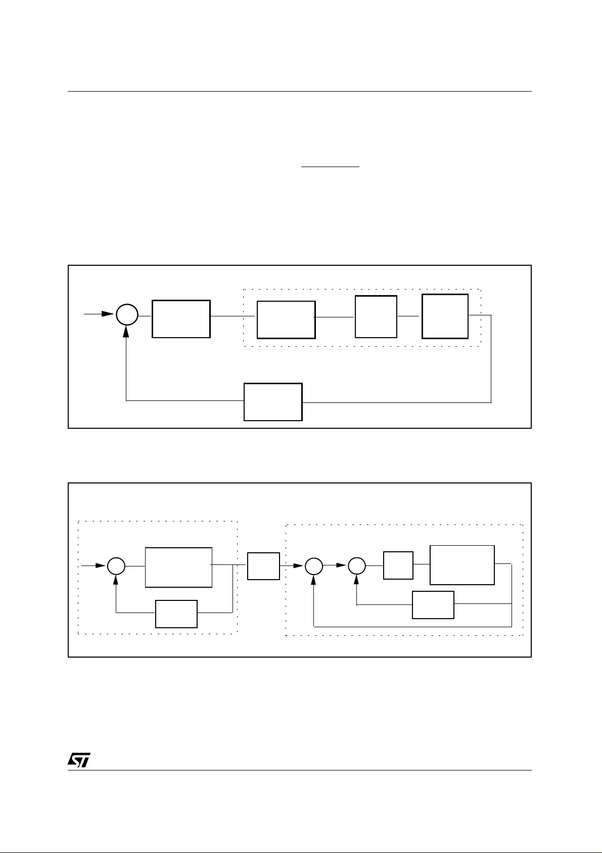
Stability Analysis of the Current Loop.
In the current sharing configuration the U1 regulator acts as a master in order to regulate the output
voltage. The second section U2 works as current follower. Its task is to deliver an output current equal to
the current delivered from the first section. For the analysis of the stability, see Fig. 21, the current loop
of the U2 section can be considered as a separated loop from the voltage loop of the U1 section, considering that the current loop is quite faster than the voltage one.
11/16
AN1126 APPLICATION NOTE
For the stability of the voltage loop see the AN938.
The open loop transfer functions is composed of the following blocks :
- Error amplifier and compensation block :
R
⋅ C
)
c
c
1
)
+
c
A
=
(s)
2
s
⋅ Ro ⋅ C
o
R
⋅
c
Avo ⋅ (1 + s ⋅
C
+ s ⋅ (Ro ⋅ Cc + Ro ⋅ Co + Rc ⋅ C
⋅
c
in which Ro = 1.2MΩ and Co = 220pF are internal capacitance and resistance of the Error Amplifier
while R
Figure 17. Error Amplifier Compensation Cir-
and Cc are the compensation values.
c
Figure 18. Output filter
cuit
L
Cc
Rogm
Rc
Co
D99IN1022
I +
Vout
Rs
Cout
ESR
RL
- Output LC filter:
Gfil
(s)
=
RL
1
+
Rs
Cout ⋅
+ s ⋅
⋅
Cout
⋅
2
Cout
s
⋅
ESR + RL) ⋅ L
(
⋅
RL + Rs
⋅
ESR
RL
(
+
Rs
RL + ESR) + L + RL ⋅ ESR ⋅ Cout
⋅ (
) +
1
RL + Rs
1
+
s
Rs is the sensing resistor, RL is the load resistance.
PWM gain:
=
Gpwm
Vcc
where Vct is the peak to peak saw tooth oscillator.
Figure 19. Current feedback.
Cint
6
+
Rint
5
R
12/16
FB
7
LM358
Vct =
⁄
Vcc
Vcc
I -
Rs
I +
⋅ 6
6
≈
1
−
Vout
Cout
Rs
Cout
AN1126 APPLICATION NOTE
The LM358 configured as an integrator introduces a gain given by Rs , a pole in Gint(s) and a zero in
Z(s) :
Vfb= ( Rs / s ⋅ Cint ⋅ Rint )[ (I
Assuming :
Gint
(s) =
and :
H(s) = (1 + s ⋅ Rint ⋅ Cint)
the current control loop block diagram can be considered as shown in Figure 20.
Figure 20. Block diagram of the current loop
+
) ⋅ (1 + s ⋅ Cint ⋅ Rint) - (I-) ]
s
Rint
⋅
1
Cint
⋅
Rs ⋅
G(s) ( Compensated E/A, PWMGain, Output Filter )
I-
Gint(s)
Current
integrator
Current
Feedback
Vfb
A(s)
Compensated
E/A
H(s)
PWM
Gain
The complete block diagram of the current sharing loop is shown is figure 21.
Figure 21. Complete block diagram of the current sharing loop
U1 section (Volt age Loop )
Vref
∆ V
Vfb
G(s)
( Compensated E/A,
PWMGain,
Output Filter )
Av
Vout
1/Rload
Iout
I-
-
I+
∆ I
Gint(s)
-
Gfilt(s)
Output
Filter
U2 section ( Current Loop )
G(s)
( Compensated E/A,
PWMGain,
Output Filter )
H(s)
I+
I+
The open loop function of the current loop is given by :
F(s) := GpwmZint(s) ⋅ Gfil(s) ⋅ A(s)
In figures 22 and 23 are shown t he open loop Gain and Phase Bode plot . The capacitor C5 does not
influence the system stability but is useful only to reduce the noise. The cut off f requency and a phase
margin are: Fc = 8KHz; Angle = 40°
13/16

AN1126 APPLICATION NOTE
Figure 22. Gain Bode open loop plot.
120
[ dB ]
100
80
60
40
20
0
-20
110100110
Figure 23. Phase Bode open loop plot.
0
[ ° ]
-20
-40
-60
-80
-100
-120
-140
-160
-180
1 10 100 1 10
| F |
f [ Hz ]
φ
F
f [ Hz ]
3
3
110
110
4
4
110
110
5
5
Figure 24. Load transient response.
14/16
Load Transient Response
Figure 24 shows the load transient behavior of the schematic circuit of Figure 15.
In Figure 24 are shown the current deliveder from the two sections, the load
current and the drop voltage on the
output . After 20µs the total current delivered from the two section is equal to
the current required from the load. So
the response time of the application is
20µs approximately for a load transient
from 1A to 6A.
TEST CONDITIONS (fig 24):
Vin = 5V, Vout = 3.3V, Load transient
form 1A to 6A, dIout/dt = 20A/µs.
AN1126 APPLICATION NOTE
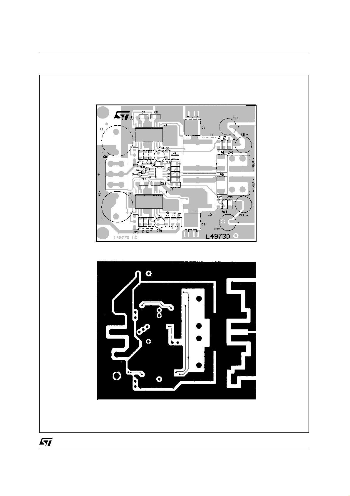
Figure 25. PCB Layout top view: Silk, component side and bottom layer (1:1.25 scale).
15/16

AN1126 APPLICATION NOTE
Information furnished is bel i eved to be accurat e and reliable. However, STMicroelec tronics assumes no responsibility for the consequences
of use of such inform ation nor for any infringement of patents or other rights of third parties which may result from its use. No license is
granted by implication or otherw ise under any patent or patent rights of STMic roelectronics . Specification mentioned in this publi cation are
subject to c hange without notice. Thi s publication supersedes and replac es all information previously su ppl ie d. S TMicroelectroni cs products
are not authorized for use as critical components in life support devices or systems without express written approval of STMicroelectronics.
The ST logo is a registered trademark of STMicroelectronics
© 1999 STMicroelectronics – Printed in Italy – All Rights Reserved
STMicroel ec tr on i c s GRO U P OF COMPANIES
Australia - Brazil - Canada - China - France - Germany - Italy - Japan - Korea - Malaysia - Malta - Mexico - Morocco - The Netherlands -
Singapore - Spain - Sweden - Switzerland - Taiwan - Thailand - United Kingdom - U.S.A.
http://www.st.com
16/16
 Loading...