

Page 1
AN1094
Application note
Solution for off-line SMPS using VIPer100-E
Introduction
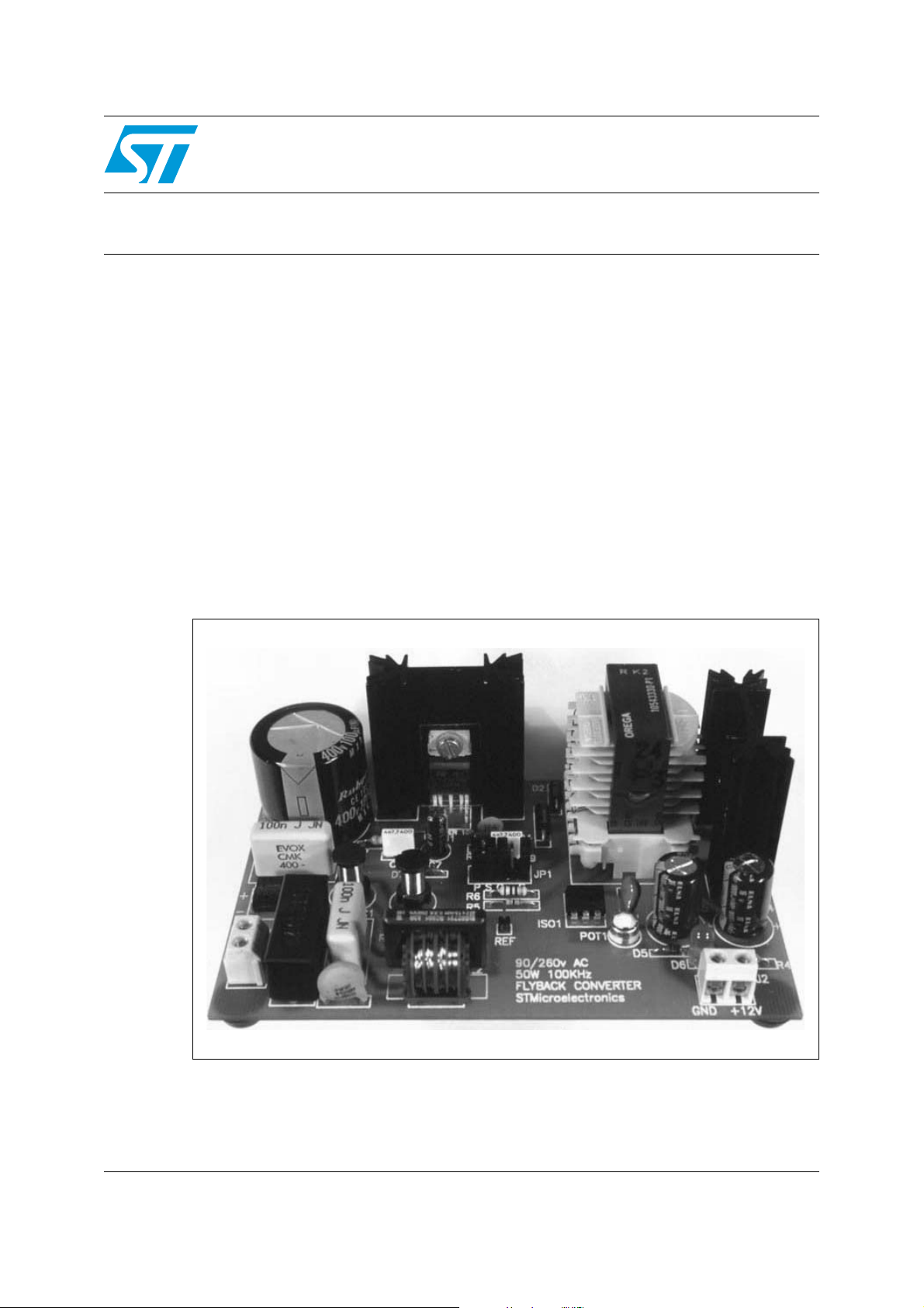
The present board prototype is a wide-range input off-line 50 W single switch Flyback,
working at 100 kHz. It is based on a new off-line smart switcher: the VIPer100-E.
The VIPer100-E is a current mode PWM with a 620 V / 2.5 Ω power switch, able to
withstand an avalanche current during normal operation. The start-up of the circuit is done
with an internal high voltage current source, which is switched off during steady state. It also
includes a regulation function designed to minimize the pin count, while maintaining design
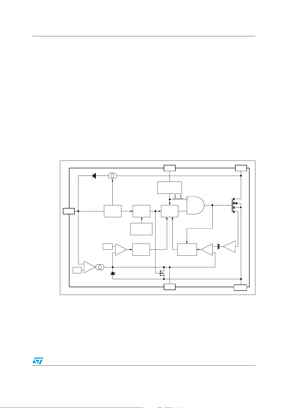
flexibility. Figure 2 presents the internal block diagram of this monolithic device. Such a
device can be easily used in any off-line flyback SMPS, with a 100 W power capability for a
single input voltage range, or 50 W with a wide input range. This stand-alone off-line Smart
Switcher concept provides a cost effective solution for SMPS for many applications such as
VCRs, TV sets, satellite receivers or decoders. The benefits for the customer are a simpler
design phase and a reduced overall components count due to the optimization of the
product configuration.
Figure 1. Standard evaluation board VIPerKITBD
October 2007 Rev 2 1/9
www.st.com
Page 2

Contents AN1094
Contents
1 VIPer100-E major features . . . . . . . . . . . . . . . . . . . . . . . . . . . . . . . . . . . . 3
1.1 VIPer100-E pin description . . . . . . . . . . . . . . . . . . . . . . . . . . . . . . . . . . . . . 4
2 Board features . . . . . . . . . . . . . . . . . . . . . . . . . . . . . . . . . . . . . . . . . . . . . . 4
2.1 Feedback loop . . . . . . . . . . . . . . . . . . . . . . . . . . . . . . . . . . . . . . . . . . . . . . 4
2.2 Special operations . . . . . . . . . . . . . . . . . . . . . . . . . . . . . . . . . . . . . . . . . . . 4
3 Schematics and board layout . . . . . . . . . . . . . . . . . . . . . . . . . . . . . . . . . . 5
4 BOM . . . . . . . . . . . . . . . . . . . . . . . . . . . . . . . . . . . . . . . . . . . . . . . . . . . . . . 7
5 Revision history . . . . . . . . . . . . . . . . . . . . . . . . . . . . . . . . . . . . . . . . . . . . 8
2/9
Page 3
AN1094 VIPer100-E major features
duc
1 VIPer100-E major features
● Adjustable Switching Frequency up to 200 kHz
● Optimized for current mode control topology
● Inherent feedforward compensation
● Soft-start and enable functions
● Overcurrent protection
● Overtemperature protection
● Overvoltage protection
● Undervoltage lock-out with hysteresis
● Low standby current
● Integrated start-up supply
● Automatic burst mode operation in standby condition
● Internally trimmed BANDGAP reference
Figure 2. Block diagram
OSC
ON/OFF
OSCILLATOR
SECURITY
LATCH
DD
V
ERROR
AMPLIFIER
_
13 V
+
UVLO
LOGIC
0.5 V
+
_
4.5 V
FF
R/S
S
OVERTEMP.
DETECTOR
1.7
µ
DELAY
PWM
LATCH
Q
s
R1
R2 R3
S
FF
Q
250 ns
BLANKING
0.5V
+
+
_
_
CURRENT
AMPLIFIER
DRAIN
1 V/A
olete Product(s) - Obsolete Pro
COMP
SOUR CE
FC00231
3/9
Page 4

Board features AN1094
1.1 VIPer100-E pin description
● VDD: this is the low level supply pin of the device. At start-up, it delivers 2 mA of
charging current. It is also connected to the inverted input of the error amplifier.
● Osc: to be connected to an external R-C network to fix the switching frequency.
● Comp: the control pin of the device. Its voltage sets the peak current of the power
switch, and it is the output of the error amplifier. As this amplifier is transconductance,
the compensation network on that pin is simply grounded.
● Drain & source: the two power pins of the device. The source is also the ground
reference of the device for compensation and oscillation networks.
2 Board features
● AC input voltage: 90 ~ 265 V
● DC output voltage / load: Vout = + 12 V, 4 A
● Operating frequency: 100 kHz
● Par. 3 gives the complete schematics of this off-line flyback converter.
2.1 Feedback loop
This evaluation board allows the user to choose between primary and secondary regulation.
Primary regulation is done through the primary auxiliary winding which delivers the low level
supply voltage on the Vdd pin of the device. This voltage represents also the secondary
output voltage, if correctly filtered in order to avoid the spikes at the beginning of each off
phase. This mode of running is achieved by putting one strap on JP1 in the "P" position.
Secondary regulation is made with an optocoupler directly from secondary output voltage. It
acts on the "COMP" pin, and the auxiliary winding is delivering the low level supply voltage
at a lower value than when in primary regulation configuration, thanks to R6. The internal
error amplifier is consequently saturated in high state, sourcing a constant current of about
0.5 mA on the "COMP" pin. To address this configuration, just put two straps on JP1 in the
"S" position. In any case, a strap in "G" position must be always present.
2.2 Special operations
No limitation has been set on the VIPer device. This limitation can be implemented on the
"COMP" pin with a zener or a Vbe multiplier, or whatever else able to clamp the voltage on
this pin at about 3 V. When the voltage is clamped, the evaluation board is able to deliver up
to 130 W of power, in continuous running. This operation must not last for more than 5
seconds. The evaluation board is fully protected against short circuits. This type of condition
leads to a burst operation, with peak current of up to 25 A on the output. As the burst duty
cycle is rather low, no risk exists and this situation can continue indefinitely. The board
withstands the no-load condition. Notice that in primary regulation, the output voltage rises
at about 20 V. Secondary regulation provides better behavior by maintaining the output
voltage at about 12 V, and has also the lowest consumption on the main lines: less than 1
watt on a 325 VDC input voltage.
maximum output power: 50 W
ac
4/9
Page 5

AN1094 Schematics and board layout
ct
Ob
3 Schematics and board layout
Figure 3. Printed board - copper side (scale 1:1)
Figure 4. Printed board - components side (scale 1:1)
e Product(s) -
rodu
5/9
Page 6

Schematics and board layout AN1094
od
Figure 5. Board schematics
J2
1
2
CON2
1k
D5
BZX55C11V
D3
POT1
D6
LED
R4
2k
C5
1000uF
16V
C4
1000uF
16V
BYW81P150
R6
10
L5
10543330-P1
OREGA
R5
4.7
C6
1nF
1kV
ISO1
4N25
PSG
D4
D2
+
D1
-
3.9k
INDUCTOR
L1
3.9k
R2
R1
DIODE ZENER
DIODE
C3
100nF
400V
C2
100uF
400V
600V, 1A
INDUCTOR
L4
D7
S
JP1
JUMPER
C9
4.7nF
R8
DRAINVDD
1N4448
-
+
23
13V
OSC
U1
VIPer100-E
1
R7
3.9k
C7
22uF
16V
54
COMP SOURCE
C8
4.7n
5.1k
C10
100nF
Product(s) - Obsolete Pr
L2
B82731-R2801-A30
SIEMENS
C1
100nF
400V
F1
1.6A
33
R3
1
2
J1
CON2
6/9
Page 7

AN1094 BOM
4 BOM
Table 1. Bill of material
Device
C1 15 0.1 µF 400 V Film
C2 10 100 µF 400 V Electrolytic, high voltage, high temp
C3 15 0.1 µF 400 V Film
C4 5 1000 µF 16 V Electrolytic, low ESR
C5 5 1000 µF 16 V Electrolytic, low ESR
C6 7.5 1 nF 400 V Ceramic high voltage - classY
C7 2 22 µF 16 V Electrolytic
C8 5 4.7 nF Film, WYMA
C9 5 4.7 nF Ceramic
C10 5 100 nF Ceramic
D1 8x5 1 A/600 V DIL diodes bridge
D2 9 BYT11-400
D3 5 BYW81/100
D4 9 BZW50-180
D5 7 BZX55C10 Zener
D6 4 GREEN LED
Pitch
(mm)
Type Description
D7 7 1N4448
F1 23 2 A FUSE
ISO1 5x8 4N25
J1 5 2contacts screw PCB connector
J2 5 2contacts screw PCB connector
L1 5 100 µH inductor 1 A rated
(1)
L2 (*) B82731-R2801-A30
L4 5 100 µH inductor 1 A rated
POT1 4+3 1 kΩ POT 3/4 turn, horizontal, miniature
R1 10 3.9 kΩ 0.25 W
R2 10 3.9 kΩ 0.25 W
R3 7.5 33 Ω NTC LCC
R4 10 2 kΩ 0.25 W
R5 10 4.7 kΩ 0.25 W
R6 10 10 Ω 0.25 W
7/9
Page 8

Revision history AN1094
Table 1. Bill of material (continued)
Device
R7 10 3.9 kΩ 0.25 W
R8 10 5.1 kΩ 0.25 W
L5 (*) OREGA 10543330-PI
1. L2 is a SIEMENS MATSUSHITA component.
2. L5 was specially developed by OREGA (THOMSON TELEVISION COMPONENT FRANCE) for this
evaluation board.
Pitch
(mm)
5 Revision history
Table 2. Document revision history
Date Revision Changes
04-Jan-2005 1 Initial release
25-Oct-2007 2
Type Description
(2)
– Document reformatted no content change
– VIPer100 replaced by VIPer100-E
8/9
Page 9

AN1094
Please Read Carefully:
Information in this document is provided solely in connection with ST products. STMicroelectronics NV and its subsidiaries (“ST”) reserve the
right to make changes, corrections, modifications or improvements, to this document, and the products and services described herein at any
time, without notice.
All ST products are sold pursuant to ST’s terms and conditions of sale.
Purchasers are solely responsible for the choice, selection and use of the ST products and services described herein, and ST assumes no
liability whatsoever relating to the choice, selection or use of the ST products and services described herein.
No license, express or implied, by estoppel or otherwise, to any intellectual property rights is granted under this document. If any part of this
document refers to any third party products or services it shall not be deemed a license grant by ST for the use of such third party products
or services, or any intellectual property contained therein or considered as a warranty covering the use in any manner whatsoever of such
third party products or services or any intellectual property contained therein.
UNLESS OTHERWISE SET FORTH IN ST’S TERMS AND CONDITIONS OF SALE ST DISCLAIMS ANY EXPRESS OR IMPLIED
WARRANTY WITH RESPECT TO THE USE AND/OR SALE OF ST PRODUCTS INCLUDING WITHOUT LIMITATION IMPLIED
WARRANTIES OF MERCHANTABILITY, FITNESS FOR A PARTICULAR PURPOSE (AND THEIR EQUIVALENTS UNDER THE LAWS
OF ANY JURISDICTION), OR INFRINGEMENT OF ANY PATENT, COPYRIGHT OR OTHER INTELLECTUAL PROPERTY RIGHT.
UNLESS EXPRESSLY APPROVED IN WRITING BY AN AUTHORIZED ST REPRESENTATIVE, ST PRODUCTS ARE NOT
RECOMMENDED, AUTHORIZED OR WARRANTED FOR USE IN MILITARY, AIR CRAFT, SPACE, LIFE SAVING, OR LIFE SUSTAINING
APPLICATIONS, NOR IN PRODUCTS OR SYSTEMS WHERE FAILURE OR MALFUNCTION MAY RESULT IN PERSONAL INJURY,
DEATH, OR SEVERE PROPERTY OR ENVIRONMENTAL DAMAGE. ST PRODUCTS WHICH ARE NOT SPECIFIED AS "AUTOMOTIVE
GRADE" MAY ONLY BE USED IN AUTOMOTIVE APPLICATIONS AT USER’S OWN RISK.
Resale of ST products with provisions different from the statements and/or technical features set forth in this document shall immediately void
any warranty granted by ST for the ST product or service described herein and shall not create or extend in any manner whatsoever, any
liability of ST.
ST and the ST logo are trademarks or registered trademarks of ST in various countries.
Information in this document supersedes and replaces all information previously supplied.
The ST logo is a registered trademark of STMicroelectronics. All other names are the property of their respective owners.
© 2007 STMicroelectronics - All rights reserved
STMicroelectronics group of companies
Australia - Belgium - Brazil - Canada - China - Czech Republic - Finland - France - Germany - Hong Kong - India - Israel - Italy - Japan -
Malaysia - Malta - Morocco - Singapore - Spain - Sweden - Switzerland - United Kingdom - United States of America
www.st.com
9/9
 Loading...