

AN1089
®
APPLICATION NOTE
CONTROL LOOP MOD ELING OF L6561-BASED TM PFC
by Claudio Adragna
This paper provides a model and a tool for evaluating and improving the control loop characteristics
of L6561-based PFC preregulators in boost topology and operated in Transition Mode (TM).
Such a subject is now becoming topical since TM PFC preregulators are more and more used in systems other than electronic lamp ballast where the input voltage range is limited and the load current
is almost constant.
The ability to operate under large variations of bot h input voltage and load current, as well as the use
of TM PFC systems as preregulators for switching converters, requires a more accurate design of the
control loop. The goal will be not only to ensure a narrow bandwidth in or der to achieve a high Power
Factor, but also to have enough phase margin so as to make sure the system is stable over a large
range of operating conditions.
INTRODUCTION
PFC preregulators based on the boost topology working in Transition Mode (TM, see fig. 1) have been
widespread in electronic lamp ballast systems. This kind of equipm ent almost always works under a single mains supply (110 or 220 VAC, with some tolerance) and the use of a PFC preregulator is mainly
aimed at optimising the downstream half-bridge lamp driver and improving their inherent extremely poor
PF.
The PFC preregulator sees the downstream stage as a constant load, so it is requested to work under a
limited range of operat ing conditions. From the control loop standpoint, this means that the frequency
compensation of the error amplifier can be very simple, t ypically just a feedback capacitor. Its capacitance will be high enough to ensure the crossover frequency of the open loop gain is low, so as to
achieve a high PF (see Ref. [1]).
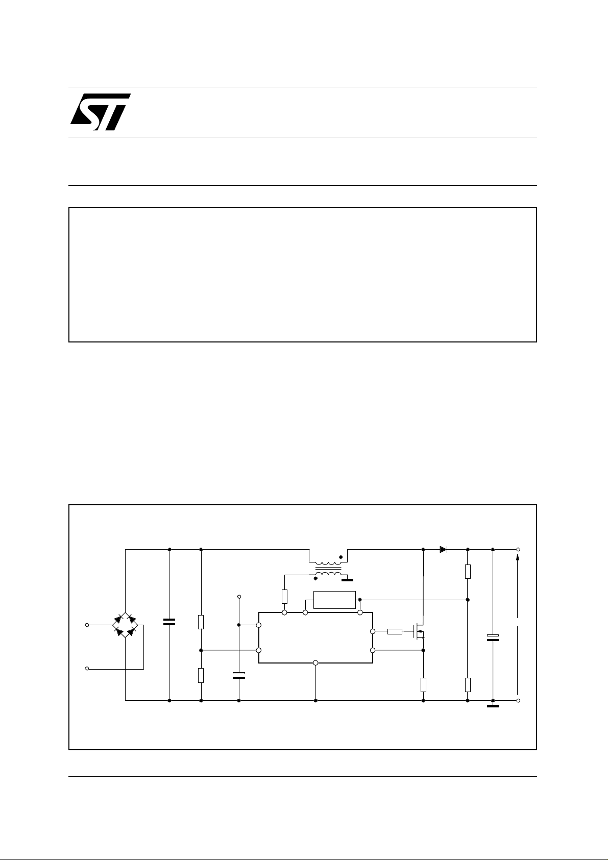
Figure 1. Typical L6561-based TM PFC preregulator
Vcc
+
-
Vac
March 2000
R9
R10
5
8
3
21
L6561
Compensation
Network
6
R7
Vo
7
4
Rs
R8
Co
1/12
AN1089 APPLICATION NOTE
Things get more complicated when an electronic ballast can supply two lamps and is required t o work
even if one lamp is not used or is exhausted, so that it is expected to work at half load as well.
The L6561, thanks to its highly linear , wide dynamics multiplier, extends the use of TM PFC boost preregulators to applications that experience a wide range of operating condit ions, both in terms of input
voltage variations and load change. High power (60 to70 W) AC-DC adapters for portable equipment
and computer monitor SMPS’ are the most noticeable examples.
This, however, calls for a more accurate design of the control loop than the one illustrated in Ref.[1]. The
control goal will no longer be to achieve only a low crossover frequency but also an adequate phase
margin. Besides ensuring stability over a large variety of operating conditions, this is necessary to prevent dangerous oscillations of the output voltage as a result of load changes.
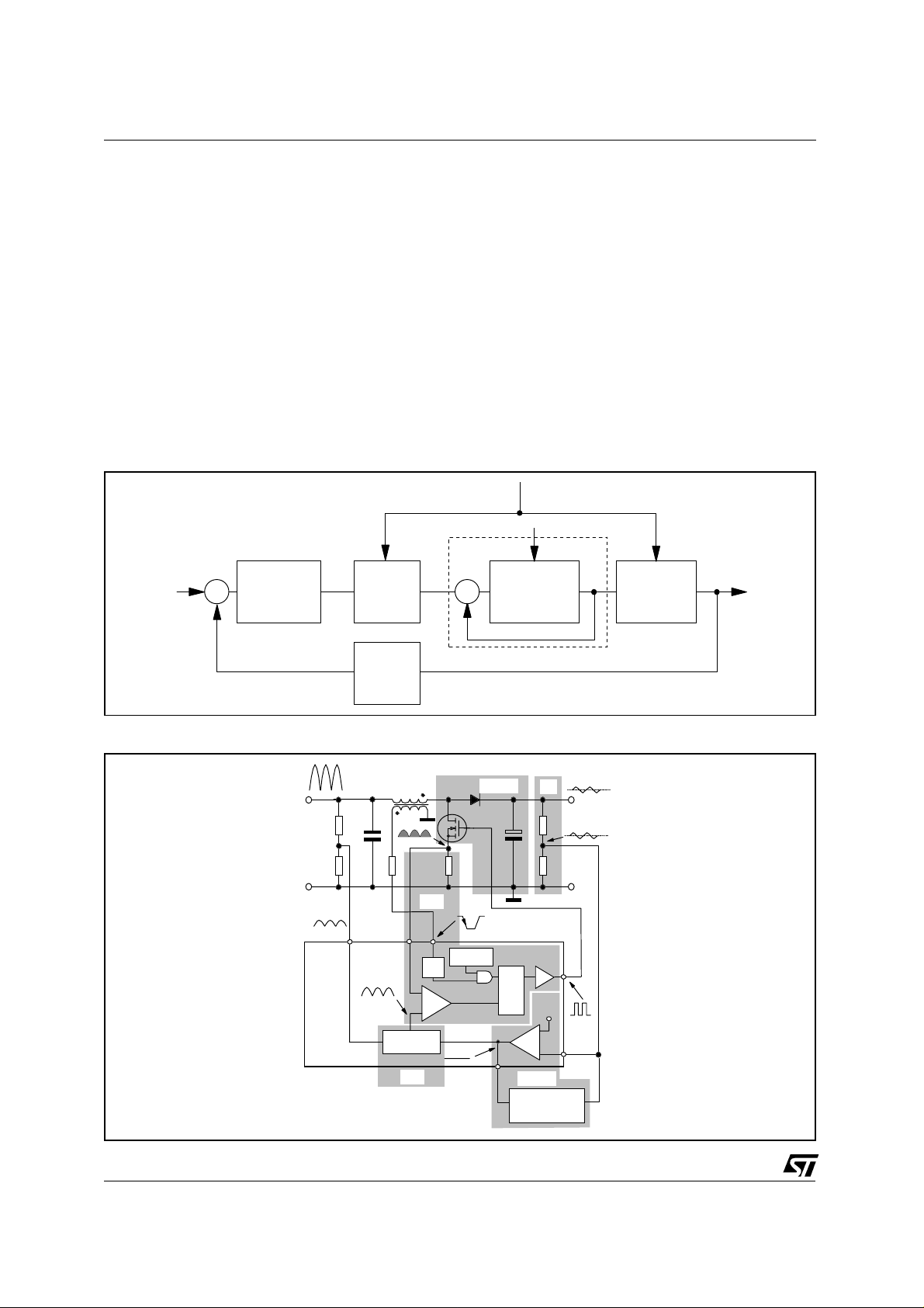
PFC Boost Preregulator Control Loop
To the aim of finding a compensation network able to achieve the above mentioned control goal, it is
necessary to get an insight into the control loop of such systems. This can be synthesised as shown in
the block diagram of fig. 2.
Figure 2. Control loop of a PFC Preregulator: Block Diagram
Virms
ZCD
G3
+
-
ERROR AMPLIFIER
G1(s)
Vref VoV
COMP
MULTIPLIER
G2
FEEDBACK
H
V
cspk
PWM MODULATOR POWER ST AG E
+
-
I
Lpk
G4(s)
Figure 3. Control loop of a PFC Preregulator: electrical circuit and main quantities
Vi
R9
R10
KP· Vi
L6561
L
V
cs
MULT CS ZCD
V
cs
MULTIPLIER
4
3
G2
Q
Rs
G3
5
STARTER
ZCD
-
PWM
+
COMPARATOR
V
G4(s)
D
Co
COMP
COMP
H
DRIVER
Q
S
VREF
R
(2.5V)
+
E/A
-
2
G1(s)
E/A
COMPENSATION
NETWORK
Vo
R7
R8
GD
7
INV
1
REF
V
2/12
AN1089 APPLICATION NOTE
Fig. 3 illustrates how the various blocks of fig. 2 relate with the electrical circuit, both external and inside
the L6561. For details on the internal circuit and its operation please refer to Ref. [1].
The loop gain of PFC preregulators must have a very low crossover frequency (fc) so as to maintain
COMP
(Error Amplifier output) fairly constant over a given line cycle and ensure a high PF.
V
As a rule of thumb, fc should not exceed 20-25 Hz at maximum mains voltage.
This allows to assume that the c ontrol action t akes place on the peak amplitude ( or, which is the same,
the RMS value) of the various quantities inside the loop.
The first step is to determine the transfer function of the power stage, G4(s), defined as:
dV
dV
G4(s) =
dI
Lpk
o
=
dI
dI
o
o
⋅
dI
o
Lpk
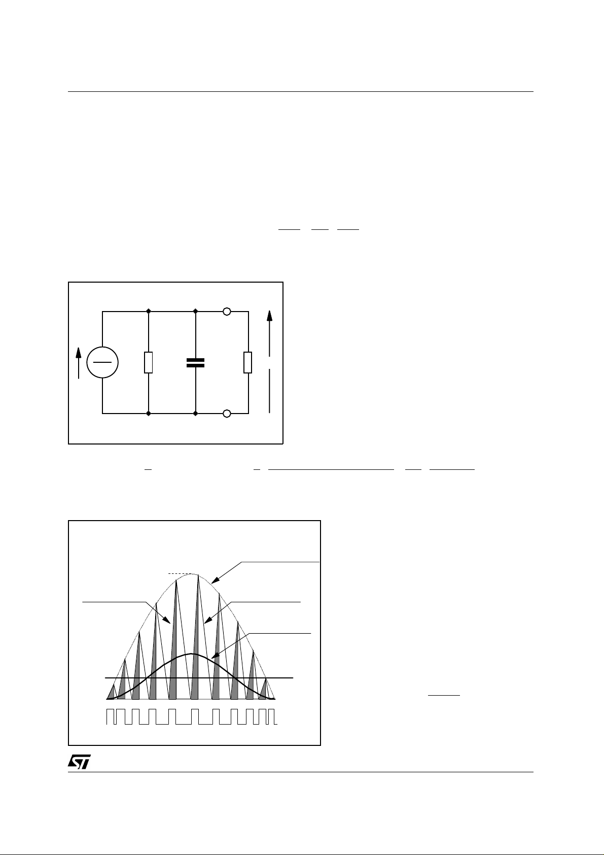
Figure 4. Power stage model,G4(s)
Io
=
I
o
Co RoRe
_________________
1
⋅
2
(1 − D) ⋅
I
Lpk
⋅ sin
Figure 5. Boost PFC currents
I
Lpk
Switch current
Vo
_________________________
√2 ⋅
1
⋅
=
θ
2
Inductor current
peak envelope
Diode current
Low frequency
Diode current
where Vo is the DC output voltage, Io the DC output
current and I
Lpk
is the peak value of the inductor cur-
rent.
Under the above assumption, the power stage can
be modeled as illustrated in fig. 4: a controlled current source (with a shunt resistor Re) t hat drives the
output bulk capacitor Co and the load resistance Ro
(= Vo / Io). The zero due to the ESR associated with
Co is far beyond the crossover frequency thus it is
neglected.
The current source can be characterised with the following considerations: the low frequency component
of the boost diode current is found by averaging the
discharge portion of the inductor current (the white
triangles of fig. 5) over a given switching cycle.
The low frequency current, averaged over a mains
half-cycle yields the DC output current Io:
V
irms
⋅ sin
V
o
θ ⋅
I
⋅ sin
Lpk
2
V
⋅
irms
⋅ I
Lpk
V
o
√
θ
=
4
where D is the switch duty cycle, θ is the instantaneous phase angle of the mains volt-
irms
age and V
its effective (RMS) value.
The AC model illustrated in fig. 4 can be
found by calculating the total differential of
the above expression of Io. A few algebraic
manipulations would show that the shunt resistor Re always equals the DC load resistance Ro, thus it changes depending on the
power delivered by the system. Now it is
necessary to consider two separate cases.
If the load is purely r esistive (or equiv alent to
a resistor, like in the case of a lamp ballast
circuit), the AC load resistance equals Ro.
The parallel of this resistance with Re, combined with the output bulk capacitor, gives
Io
origin to a pole located at:
SWITCH
ON
OFF
2
=
ω
p
R
⋅ C
o
o
which is usually in the range of 1 to 5 Hz.
3/12
AN1089 APPLICATION NOTE
In case the PFC preregulator provides a DC bus supplying a downstream switching converter, the load
should be regarded as a "constant power" load rather than a resistor. In fact, as long as a switching converter is in regulation, the power it demands of the source is practically independent of the input voltage
(converter’s efficiency changes very little).
In this case, the AC load resistance is equal to -Ro (if the DC bus decreases the current demanded of
the PFC increases, whence the negative sign). As a result, the parallel combination with Re tends to infinity and the two resistances cancel. The current source drives only the output capacitor and the pole location tends to zero. In the end, G4(s) will be given by:
2
√
V
irms
⋅
⋅
V
o
V
irms
⋅
⋅
V
o
G4(s) =
8
2
√
4
The gain of the PWM modulator, G3, which includes the current loop, is simply:
R
o
R
1 + s ⋅
1
.
(constant power load
s ⋅C
o
(resistive load)
⋅ C
o
o
2
)
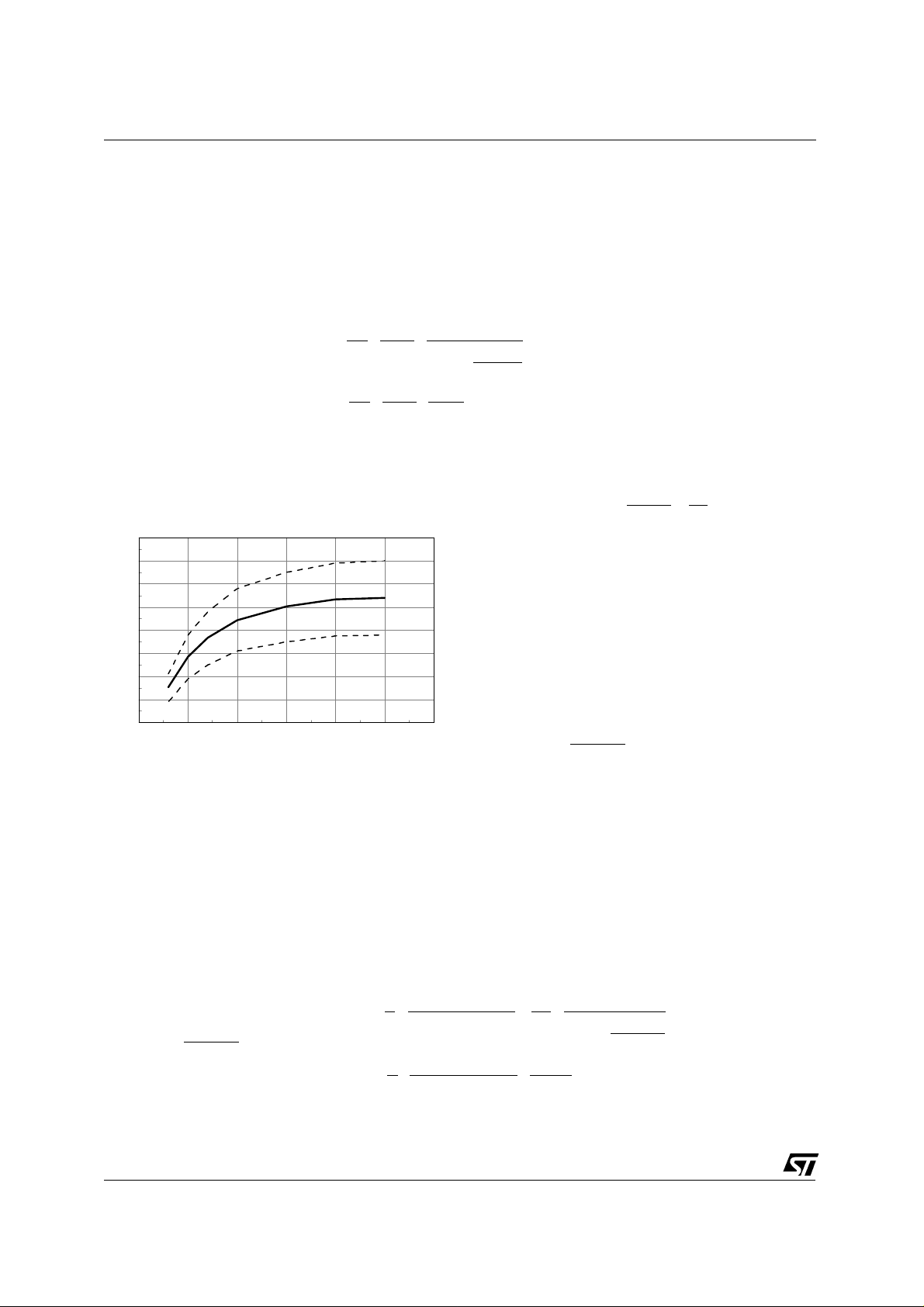
Figure 6. Plot of KM vs. E/A output
KM
0.9
0.8
0.7
0.6
0.5
0.4
0.3
0.2
0.1
2.5 3 3.5 4 4.5 5 5.5
VCOMP
where Rs is the sense resistor connected between the source of the external MOSFET and
ground (across which the L6561 reads the inductor current through pin 3).
To calculate the transfer function G2 of the multiplier block, one can consider that a variation
COMP
V
∆
, due to a line and/or load change, modifies the peak amplitude Vcspk of the rectified
sinusoid at the output of the multiplier.
Therefore:
dV
G2 =
dV
G3 =
cspk
COMP
dI
Lpk
=
dV
cspk
R
= KM ⋅ KP ⋅
1
s
V
√2⋅
irms
where KM is the gain of the multiplier and KP the partition ratio of the resistor divider that feeds a portion
of the input voltage into pin 3.
The electrical characteristics of the L6561 specify K
but actually KM decreases for low values of V
COMP
along with the tolerance limits. Since V
V
M
ation of K
partly compensates for t he increase of G2 with V
COMP
COMP
M
= 0.6 ±25% (@V
. In fig. 6 t he typical value of KM is plotted against
gets lower when the mains voltage is high, this vari-
irms
COMP
= 4V, including temperature)
, thus providing a mild voltage feedforward effect.
If one wants to take this non-linearity into account, he or she should linearise the large-signal multiplier
gain in the neighborhood of the quiescent point of the error amplifier, so as to get the small-signal gain
(km). Please refer to [1] and the Appendix for the relevant calculation technique.
Ultimately, the control-to-output transfer function will be:
⋅ V
P
V
O
⋅ V
P
Rs ⋅ V
2
O
irms
2
irms
⋅
⋅
R
o
R
s
1
s ⋅ C
⋅
1 + s ⋅
O
G(s) =
dV
dV
O
= G2 ⋅ G3 ⋅ G4(s) =
COMP
km ⋅ K
1
⋅
4
km ⋅ K
1
⋅
2
where the small-signal multiplier gain km could be assumed equal to K
4/12
1
R
(resistive load
⋅ C
O
O
2
(constant power load
for simplicity.
M
)
)

AN1089 APPLICATION NOTE
Figure 7. Typical compensation scheme in
PFC preregulators for lamp ballast
Vo
C3
R7
1
INV
R8
2.5V
2
_
E/A
+
TO MULTIPLIER
L6561
From the above equations, it is apparent that the gain
of the control-to-output function is strongly dependent
on the input voltage, despite the slight compensation
M
provided by K
. For design purpose, G(s) will have to
be considered at the maximum mains voltage, where
the gain is maximum and the loop bandwidth is maximum as well.
The feedback block is usually made up of a simple
resistor divider (see fig. 7). Only the upper resistor R7
is significant to the loop gain (the lower resistor R8
just sets the value of Vo). It is then convenient to assume H=1 and to consider R7 as a part of the error
amplifier block G1(s).
Error Amplifier Compensation
In PFC preregulators that supply an electronic lamp ballast the error amplifier is compensated typically
as shown in fig. 7 (see also Ref. [2] and [3]).
For this kind of load this circuit gives satisfactory results. It may not be acceptable, however, in other
systems where stability must be ensured over a wide range of input voltage and load current, and does
not work at all when the PFC preregulator supplies a switching converter.
Figure 8 shows the suggested compensation schemes for both the cases under consideration.
With a resistive load the loop can be stabilised by adding a pole in the origin plus a low frequency zero
that compensates the pole of the control-to-output gain (network a). Ideally, this can give the desired
bandwidth with 90° phase margin as well as high DC gain for good load regulation.
With a constant power load the control-to-output gain has a pole in the origin thus the DC gain of the error amplifier should be externally limited with a feedback resistor. If not, a second pole in the origin
would be introduced, which would result in a system whose stability might be critical.
Limiting the gain goes to t he detriment of preregulator’s load regulation but this has not a serious impact
on the overall system since the downstream converter will easily compensate for that.
The compensation network (b) adds a pole-zero couple that both makes the gain roll off at low frequency
(so as to cross the 0 dB axis at low frequency) and boosts the phase in the neighborhood of the crossover frequency (so as to increase phase margin).
The transfer functions of the compensation networks of fig. 8 a) and b) are respectively:
1 + s ⋅ C3 ⋅ R11
G1(s) =
dV
COMP
dV
s ⋅ C3 ⋅ R7
=
O
R12
⋅
R7
1 + s ⋅ C3 ⋅ (R11 + R12
(circuit a − resistive load
1 + s ⋅ C3 ⋅ R11
(circuit b − constant power load
)
Figure 8. Suggested compensation networks for TM boost PFC
Vo
R11
R7
R8
C3
COMP
1
INV
2.5V
a) resistive load b) constant power load
2
_
E/A
+
TO MU LTIP LI ER
L6561
Vo
R7
R8
INV
)
)
R12
R11
C3
1
_
E/A
+
2.5V
COMP
2
TO MU LTIP LI ER
L6561
5/12

AN1089 APPLICATION NOTE
As a tool to ease the design of L6561’s E/A compensation networks in TM boost PFC preregulators, the
Appendix contains a Mathcad® file gathering the theory above illustrat ed and performing all the necessary calculations.
Conclusions
This paper gets an insight into the control loop of TM controlled Boost PFC preregulators based on the
L6561 PFC controller. This reveals that the simple feedback capacitor used to compensate the error amplifier in preregulators for lamp ballast may not be adequate in systems that may experience large variations in input voltage and/or load current. Moreover it leads to an unstable loop if the load is a switching
converter. Appropriate compensation schemes are suggested for both cases and a calculation tool
(Mathcad® file) is provided so as to make control loop design easier in such systems.
References
[1] "L6561, Enhanced Transition Mode Power Factor Corrector", (AN966)
[2] "L6569 - L6561 Lighting Application with PFC" (AN991)
[3] "Electronic Ballast with PFC Using L6574 and L6561" (AN993)
[4] "Design Equations of High-Power-Factor Flyback Converters Based on the L6561" (AN1059)
[5] "Flyback Converters with the L6561 PFC Controller" (AN1060)
Appendix
This Mathcad® file allows to design the control loop and performs a stability analysis of PFC preregulators in boost topology operated in Transition Mode and controlled by the L6561.
Highlighted equations indicate data that must be manually entered. These data are supposted to be
known to the user as a result of the design of the PFC preregulator (the use of the PFC design software
included in the CD-ROM "Linear and Switching Voltage Regulators" is recommended). The example values are taken from the L6561 demo board circuit.
PFC Converter Data:
Output Voltage V
Output Capacitor C
Sense Resistor R
O
:= 400 V
O
:= 47
s
:= 0.41
Output Overvoltage Threshold OVP := 40 V
Expected Efficiency
:= 0.9
η
Multiplier Biasing:
Input Divider Upper Resistor R
Input Divider Lower Resistor R
up
:= 1240 k
low
:= 10 k
Analysis Setpoint:
irms
Mains RMS Voltage V
Output Power P
:= 264 V
O
:= 80 W
F
µ
Ω
Ω
Ω
6/12

Preliminary calculations & Service Variables:
Equivalent Load Resistance
Input Divider Gain
R
KP
o
:=
Large-signal Multiplier Gain: KM(V
2
V
O
RO = 2 ⋅10
P
O
R
:=
low
R
low
COMP
KP = 8 ⋅10
+ R
up
) := 0.651 ⋅ (1 - 85.29 ⋅ e
AN1089 APPLICATION NOTE
3
-3
-1.776 ⋅ VCOMP
Ω
)
Error Amplifier Quiescent Point: V
V
COMP
:
=
root
2.5
+
KM(V
η ⋅
V
Small signal Multiplier Gain
:= 4
COMP
R
Po ⋅
2
⋅
COMP
COMP
km
S
KP
) ⋅
V
⋅
irms
= 2.898 [V]
d
:
=
dV
COMP
[KM(V
− V
2
COMP
COMP
) ⋅
(
, V
V
COMP
COMP
−
2.5
]
)
km = 0.557
---------- -------------------------------------------- --------------------------------------------- ---------------------- -----------------
Dec
w ⋅
− 1
j: = √ -1 n: = 100 Dec: = 6 w:= 0,1..n
(w): = 10
ω
f: = 1
n
Control-to-Output Transfer Function (constant power load):
6
10
j ⋅ ω ⋅ C
O
/G
150
100
¦G¦
G
(ω)
km ⋅ KP ⋅ V
: =
2 ⋅ V
2
⋅
1
⋅
R
S
89
irms
O
50
dB
0
50
0.1 1 10 100 1.10
f
3
90
deg
91
0.1 1 10 100 1.10
f
Compensated E/A Transfer Function (constant power load, refer to fig.8b)
O
DC gain (∆V
/∆V
COMP
): GO := 0.30
Pole: p := 0.23 Hz
Zero: z := 15 Hz
3
7/12

AN1089 APPLICATION NOTE
Transfer Function: G1
(ω) :=
0
20
dB
40
60
0.1 1 10 100 1.10
¦G1¦
3
f
Open Loop Transf e r Func tion (constant powe r loa d):
F(ω): = G (ω) ⋅ G1 (ω)
1 + j ⋅
GO ⋅
1 + j
0
20
40
deg
60
80
100
0.1 1 10 100 1.10
ω
z
2
⋅ π ⋅
ω
⋅
2
p
⋅ π ⋅
/G1
f
3
): = arg (F(ω)) ⋅
ΦF(ω
100
0
dB
100
0.1 1 10 100 1.10
¦F¦
f
40
80
deg
120
160
3
200
Crossover Frequency: fc: = |root (|F(2
fc = 18.836 Hz
Phase Margin:
: = 180 + ΦF
Φ
= 52.167 °
Φ
180
π
0
0.1 1 10 100 1.10
f)| - 1, f)|
⋅ π ⋅
fc)
(2 ⋅ π ⋅
/F
f
3
8/12

AN1089 APPLICATION NOTE
Feedback Network Implementation (constant power load, refer to fig. 8b):
OVP
Output Divider Upper Resistor
R7:
=
40
⋅ 103
R7 = 1 ⋅ 10
R8:
Output Divider Lower Resistor
=
V
Parallel Feedback Resistor: R12: = G
C3:
Series Feedback Capacitor
=
2
C3 = 2.271 ⋅ 10
Series Feedback Resistor R11: =
2
Control-to-Output Transfer Function (resistive load):
2
irms
R
O
⋅
⋅
R
s
100
G
(ω)
km ⋅ KP ⋅ V
: =
4 ⋅ V
O
¦G¦
3
2.5
⋅ R7 R8 = 6.289 k
2.5
−
O
O
⋅ R7 R12 = 300 k
6
10
R12
⋅ π ⋅
3
6
10
z
C3
⋅
⋅ π ⋅
1 + j ⋅ ω ⋅ C
0
1
1
⋅
⋅
z
p
R11 = 4.672 k
1
R
O
⋅
O
2
⋅ 10
6
−
/G
k
nF
Ω
Ω
Ω
Ω
50
dB
0
50
0.1 1 10 100 1.10
f
Pole Location: p :
20
40
deg
60
80
π ⋅
100
0.1 1 10 100 1.10
f
6
10
R
p = 3.386 Hz
⋅ C
O
O
3
9/12
3
=

AN1089 APPLICATION NOTE
Compensated E/A Transfer Function (resistive Load, refer to fig. 8a):
High Frequency Gain: G
Zero: z := 15 Hz
Transfer Function: G1
h
:= 0.005
(ω) :=
G
ω
j
1 +
⋅
z
2
2
⋅
h
⋅
π ⋅
z ⋅
⋅ π ⋅
j
⋅
ω
20
0
20
dB
40
60
0.1 1 10 100 1.10
¦G1¦
f
0
20
40
deg
60
80
3
100
0.1 1 10 100 1.10
/G1
f
Open Loop Transfer Function (resistive load)
3
F(ω): = G(ω) ⋅ G1(ω)
180
0
40
80
deg
120
160
200
0.1 1 10 100 1.10
100
50
0
dB
50
100
0.1 1 10 100 1.10
¦F¦
f
): = arg (F(ω)) ⋅
ΦF(ω
3
Crossover Frequency: fc: = |root (|F(2
fc = 19.805 Hz
π
⋅ π ⋅
/F
3
f
f )| - 1, f)|
10/12

AN1089 APPLICATION NOTE
Phase Margin:
: = 180 + ΦF
Φ
= 62.563 °
Φ
(2 ⋅ π ⋅
Feedback Network Implementation (resistive load, refer to fig. 8a):
OVP
Equivalent Load Resistance
Output Divider Lower Resistor
Series Feedback Capacitor
Series Feedback Resistor R11: =
R7:
R8:
C3:
=
=
=
⋅ 103 R7 = 1 ⋅10
40
V
2
O
⋅ π ⋅
2
2.5
−
⋅
2.5
6
10
z ⋅ Gh ⋅ R7
6
10
z ⋅ C3
⋅ π ⋅
R7 R8 = 6.289
R11 = 5 k
fc)
C3 = 2122 ⋅ 10
3
k
Ω
k
Ω
3
nF
Ω
11/12

AN1089 APPLICATION NOTE
Information furnished is bel i eved to be accurat e and reliable. However, STMicroelec tronics assumes no responsibility for the consequences
of use of such inform ation nor for any infringement of patents or other rights of third parties which may result from its use. No license is
granted by implication or otherw ise under any patent or patent rights of STMic roelectronics . Specification mentioned in this publi cation are
subject to c hange without notice. Thi s publication supersedes and replac es all information previously su ppl ie d. S TMicroelectroni cs products
are not authorized for use as critical components in life support devices or systems without express written approval of STMicroelectronics.
The ST logo is a registered trademark of STMicroelectronics
© 2000 STMicroelectronics – Printed in Italy – All Rights Reserved
STMicroel ec tr on i c s GRO U P OF COMPANIES
Australia - Brazil - China - Finland - France - Germany - Hong Kong - India - Italy - Japan - Malaysia - Malta - Morocco -
Singapore - Spain - Sweden - Switzerland - United Kingdom - U.S.A.
http://www.st.com
12/12
 Loading...