

Page 1
AN1088
®
APPLICATION NOTE
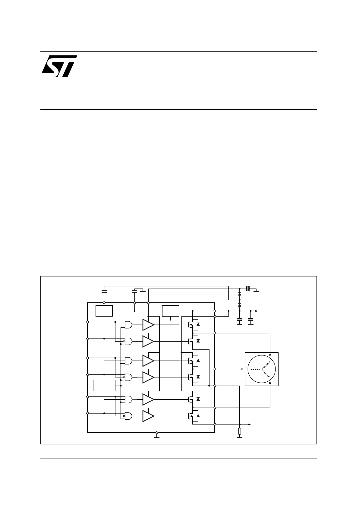
L6234 THREE PHASE MOTOR DRIVER
by Domenico Arrigo
INTRODUCTION
The L6234 is a DMOSs triple half-bridge driver with input supply voltage up 52V and output current of
5A. It can be used in a very wide range of applications.
It has been realized in Multipower BCD60II technology which allows the combination of isolated DMOS
transistors with CMOS and Bipolar circuits on the same chip. It is available in Power DIP 20 (16+2+2)
and in Power SO 20 packages.
All the inputs are TTL/CMOS compatible and each half bridge can be driven by its own dedicated input
and enable.
The DMOS structure has an intrinsic free wheeling body diode so the use of external diodes, which are
necessary in the bipolar configuration, can be avoided. The DMOS structure allows a very low quiescent
current of 6.5 mA typ. at Vs=42V , irrespective of the load.
DEVICE DESCRIPTION
The device is composed of three channels. Each channel is composed of a half bridge with two power
DMOS switches ( typ. Rdson of 300mW @ 25°C) and intrinsic free wheeling diodes. Each channel includes two TTL/CMOS and uP compatible comparators, and a logic block to interface the inputs with the
drivers. The device includes an internal bandgap reference of 1.22V, a 10V voltage reference to supply
the internal circuitry of the device, a central charge pump to drive the upper DMOS switch, thermal shutdown protection and an internal hysteretic function which turns off the device when the junction temperature exceeds approximately 160 °C. Hysteresys is about 20 °C.
Figure 1. L6234 Block Diagram
April 2001
IN1
EN1
IN2
EN2
IN3
EN3
C3
10nF
CHARGE
PUMP
THERMAL
PROTECTION
1µF
VREFVCP
C4 220nF
C5
VBOOT
T1
T2
T3
T4
T5
T6
Vs
Vs C2
OUT1
OUT2
SENSE1
OUT3
SENSE2
D98IN940A
100nF
GND
V
10V
REF
D2
1N4148
D1
1N4148
100µF
BRUSHLESS
MOTOR
WINDINGS
R
SENSE
Vs
C1
1/14
Page 2
]
AN1088 APPLICATION NOTE
PIN DESCRIPTION.
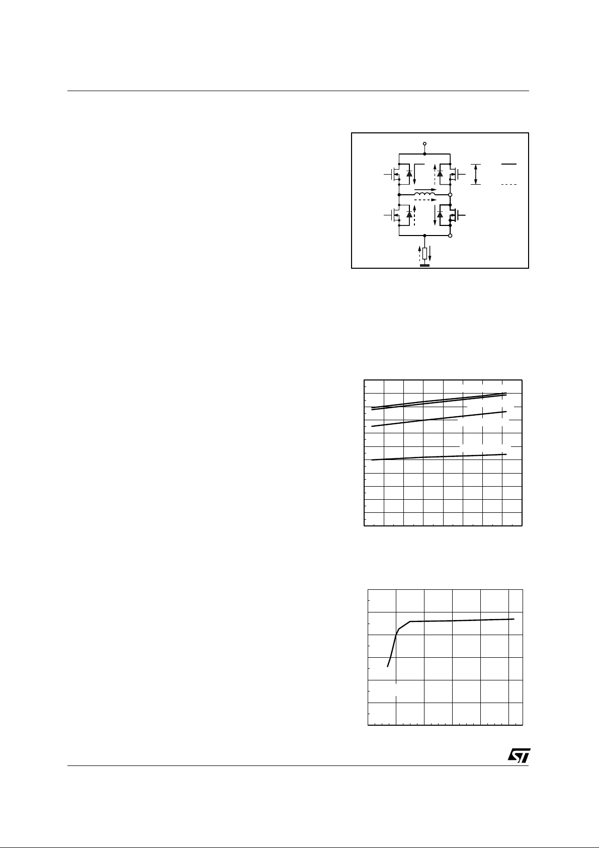
Vs ( INPUT SUPPLY VOLTAGE PINS).
Figure 2.
V
S
These are the two input supply voltage pins. The unregulated
input DC voltage can range from 7V to 52V.
With inductive loads the recommended operating maximum
supply voltage is 42V to prevent overvoltage applied to the
DMosfets. In fact considering a full bridge configuration (see
ON/OFF
T1
L
B
-V
F
T3
C
(VS+VF)
ON
V
F
OFF
fig. 2), when the br idge is switched of f (ENABLE CHOPPING)
the current recirculation produces a negative voltage to the
source of the lower DMOS switches (point A). In this condition the drain-source voltage of T
Dinamically V
slope, dI/dt, and also V
can be same Volts depending on the current
F
sense
and T4 is VS + VF + V
1
sense
, depending on the parasitic in-
ductance and current slope can be some Volts. So the drain-
T2 T4
.
-V
A
SENSE
Rsense
ON/OFF
S
D98IN938A
source voltage of T1 and T4 DMOS switches can reach more
than 10V over the V
voltage. The input capacitors C1 and C2 are chosen in order to reduce overvoltage
S
due to current decay and to parasitic inductance. For this reason C2 has to be placed as closed as possible to V
and GND pins.
S
The device can sustain a 4A DC input current f or each of the two Vs pi ns, in accordance with the
power dissipation.
Figure 3. Reference Voltage vs.
OUT1, OUT2, OUT3 (OUTPUTS).
These are the output pins
that correspond to the mid point of each half bridge. They are
designed to sustain a DC current of 4A.
SENSE1, SENSE2.
SENSE1 is the common source of the lower DMOS of the half
bridge 1 and 2.
SENSE2 is the source of the lower DMOS of the half bridge
3.
Each of these pins can handle a current of 5A.
A resistance, Rsense, connected to these pins provides feed-
back for motor current control.
Care must be taken with the negative voltage applied to these
pins : negative DC voltage lower than -1V could damage the
device. For duration lower than 300ns the device can sustain
pulsed negative voltage up to -4V.
For example, if enable chopping current control method is
used, negative voltage pulses appear to these pins, due to the
current recirculation through the sensing resistor.
Vref ( Voltage Reference).
This is t he internal 10V voltag e reference pi n to bias the log ic
and the lo w volt a ge circu it ry of the d evic e. A 1µF electrolytic capacitor connected from this pin to GND ens ur es the s tability of the
Vref [V]
11
10
9
8
7
6
5
4
3
2
1
0
-50 -25 0 25 50 75 100 125 150
Figure 4. Reference Voltage vs.
Vref [V]
12
10
8
Junction Temperature.
Vs = 52V
Vs = 24V
Vs = 10V
Vs = 7V
Tj [°C]
Supply Voltage.
DMOS drive circuit. This pin can be externally loaded up to 5mA .
Figure 3 and 4 show the typical be havior of the Vref pin.
6
4
Vcp ( CHARGE PUMP ).
Tj = 25°C
2
This is the internal oscillator output pin for the charge pump.
The oscillator supplied by the 10V Voltage Reference
switches from GND to 10V with a typical frequency of
2/14
0
01020304050
Vs [V
Page 3

AN1088 APPLICATION NOTE
1.2MHz (see fig 4). When the oscillator output is at ground , C3 is charged by Vs through D1. When it
rises to 10V, D1 is reverse biased and the charge flows from C3 to C4 through D2, so the Vboot pin after a few cycles reaches the maximum voltage of Vs + 10V - VD1- VD2.
Vboot ( BOOTSTRAP).
This is the input bootstrap pin which gives the overvoltage nec essary to dr iv e all the upper DMOS of the
three half bridges (see fig 5).
Figure 5. Charge Pump Circuit.
Vs
C1
C2
100µF
0.1µF
Vs
Vs-VD1
Vs+Vref-VD1
f=1.2 MHz
VCP
D1
1N4148
C3
10nF
Vref
D2
1N4148
Vs+Vref-VD1-VD2
C4
0.22µF
VBOOT
CHARGE
PUMP
f=1.2 MHz
Vref
10V
HIGH
SIDE
DRIVER
OUT
SENSE
LOGIC INPUTS PINS.
EN1, EN2, EN3 (ENABLES).
These pins are TTL/CMOS and µP compatible. Each half bridge can be enabled by its own dedicated
pin with a logic HIGH. The logic LOW on these pins switches off the related half bridge (see Fig. 6). The
maximum switching frequency is 50kHz.
Figure 6. Control logic for each half bridge.
INPUT
ENABLE
UPPER
DMOS
LOWER
DMOS
low level
high level
DMOS OFF
DMOS ON
high level
high level
DMOS ON
DMOS OFF
low level
low level
DMOS OFF
DMOS OFF
high level
low level
DMOS OFF
DMOS OFF
time
time
time
time
Figure 7. Cross Conduction Protection.
DMOS ON
tdelay
DMOS OFF
high level
low level
tdelay
300ns
DMOS OFF
DMOS ON
INPUT
PIN
UPPER
DMOS
LOWER
DMOS
low level
DMOS OFF
300ns
DMOS ON
time
time
time
IN1, IN2, IN3 (INPUTS).
These pins are TTL/CMOS and µP compatible. They allow switching on the upper DMOS ( INPUT at
high logic level) or the lower Dmos (INPUT at low logic level) in each half bridge (see Fig. 6).
3/14
Page 4
AN1088 APPLICATION NOTE
Cross conduction protection (see Fig. 7) avoids simultaneously turning on both the upper and lower
DMOS of each half bridge. There is a fixed delay time of 300ns between the turn on and the turn off of
the two DMOS switches in each half bridge. The switching operating frequency is up 50kHz. High commutation frequency permits the r eduction of ripple of the output current but increa ses the device’s power
dissipation, however low commutation frequency causes high ripple of the output current. The switching
frequency should be higher than 16kHz to avoid acoustic noises.
The sink current at the INPUTS and ENABLES pins is approximately 30µA if the voltage to these pins is
at least 1V less than the Vref voltage (see Fig. 3 and Fig. 4). To avoid overload of the logic INPUTS and
ENABLES , voltage should be applied to Vs prior to the logic signal inputs.
POWER DISSIPATION
An evaluation of the power dissipation of the I C driving a three phase motor in a chopping current control application follows.
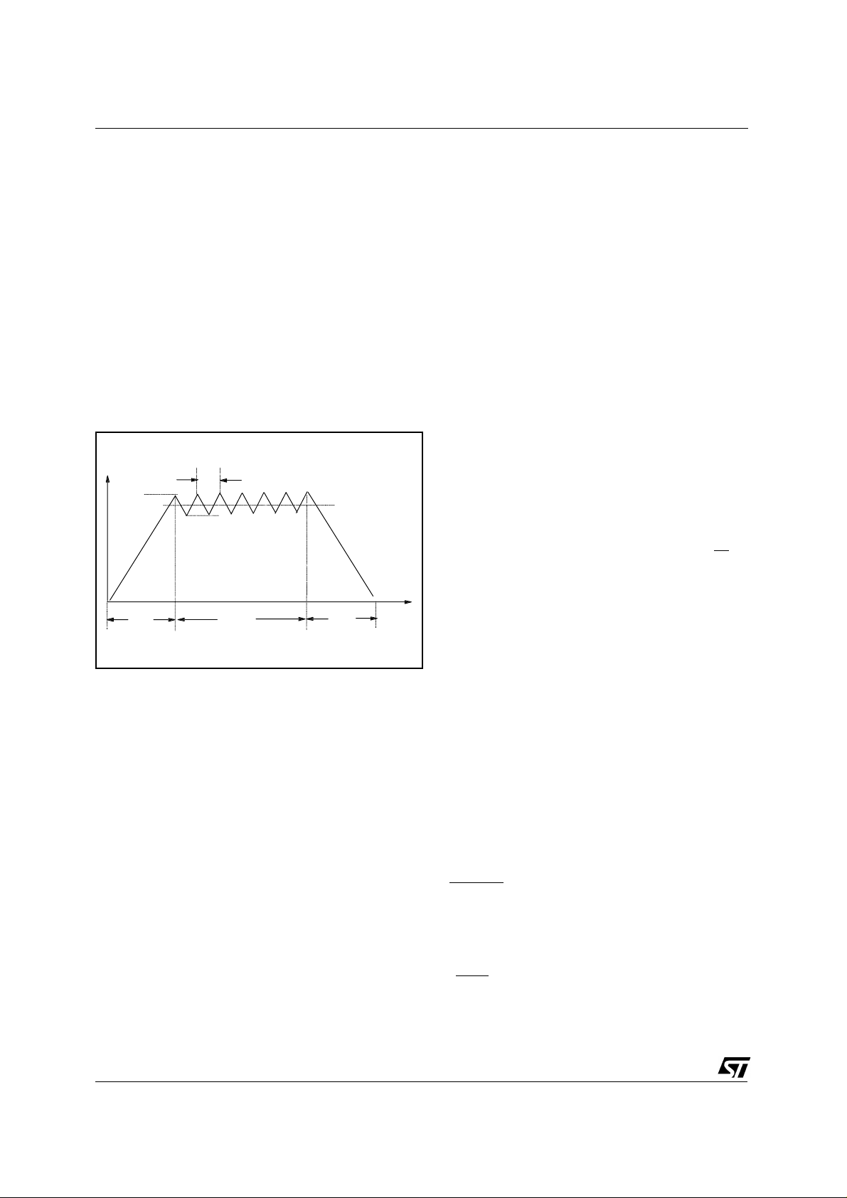
With a simplified approach it can be distinguished three periods (see Fig. 8) :
Figure 8.
Rise Time, Tr, period.
This is the rise time period, Tr, in which the current switches from one winding to another. In this
Tchop
Ipk
Iload
Ival
time a DMOS is switched on and the current increases up to the peak value Ipk with the law i(t)
= (Ipk/Tr) t. T he energy lost for t he rise time in
the period T is :
Erise =
Tr
Rdson ⋅ i
∫
0
2
dt = Rdson ⋅ I
(t)
2
pk ⋅
Tr
3
Fall Time,Tf, period.
Trise
Tload
Tfall
When the current switches from one winding to
another, there is a fall time in which the current
that flows in the intrisic diode of the DMOS decreases from Ipk to zer o. If VD is t he voltage fall
of the diode, the energy lost is :
tf
Efall =
VD(t) ⋅ i(t)dt
∫
0
Tload
During this time the current that flows in the winding is limited by the chopping current control. The energy dissipated due to the ON resistance of the DMOS is :
Eload = Rdson ⋅ (I
rms
2
⋅ Tload
)
In the formula, Irms is the RMS load current, given by :
Irms =
Iload
(
2
+
)
√
I
pk
2
3
√
− Ival
and Iload is the average load current.
When the switch is ON, the energy dissipated due to the commutation of the chopping current control in
the DMOS can be assumed to be:
Eon = Vs ⋅ Ival ⋅
tcom
2
where tcom is the commutation time of the DMOS switch.
4/14
Page 5
AN1088 APPLICATION NOTE
When the switch is OFF :
Eoff = Vs ⋅ Ipk ⋅
tcom
2
The energy lost by commutation in a chopping period, given by Eon + Eoff, is :
Ecom = Vs ⋅ Iload ⋅ tcom
The energy lost by commutation during the Tload time is given by :
Ecom = Vs ⋅ Iload ⋅ tcom ⋅ Tload ⋅ fchop
Quiescent Power Dissipation, Pq.
The power dissipation due to the quiescent current is Pq = Vs ⋅ Iq , in which Iq is the quiescent current
at the chopping frequency, fchop = 1/Tchop.
Total Power Dissipation
.
Let’s evaluate the power dissipation of the device driving a three phase brushless motor in chopping current control. In the driving sequence only one upper DMOS and a lower one are on at the same time
(see fig. 9 and 10). The total power dissipation is given by :
2 ⋅ (Erise + Efall + Eload + Ecom
Ptot =
T
)
+ Pq
Figure 11 shows the total power dissi pation, Pd, of the L6234 driving a three phase brushless motor in
input chopping current control at different chopping frequency.
EVALUATION BOARD.
The L6234 Power SO20 board has been realized to evaluate the device driving, in closed loop control, a
three phase brushless motor with open collector Hall effect sensors.
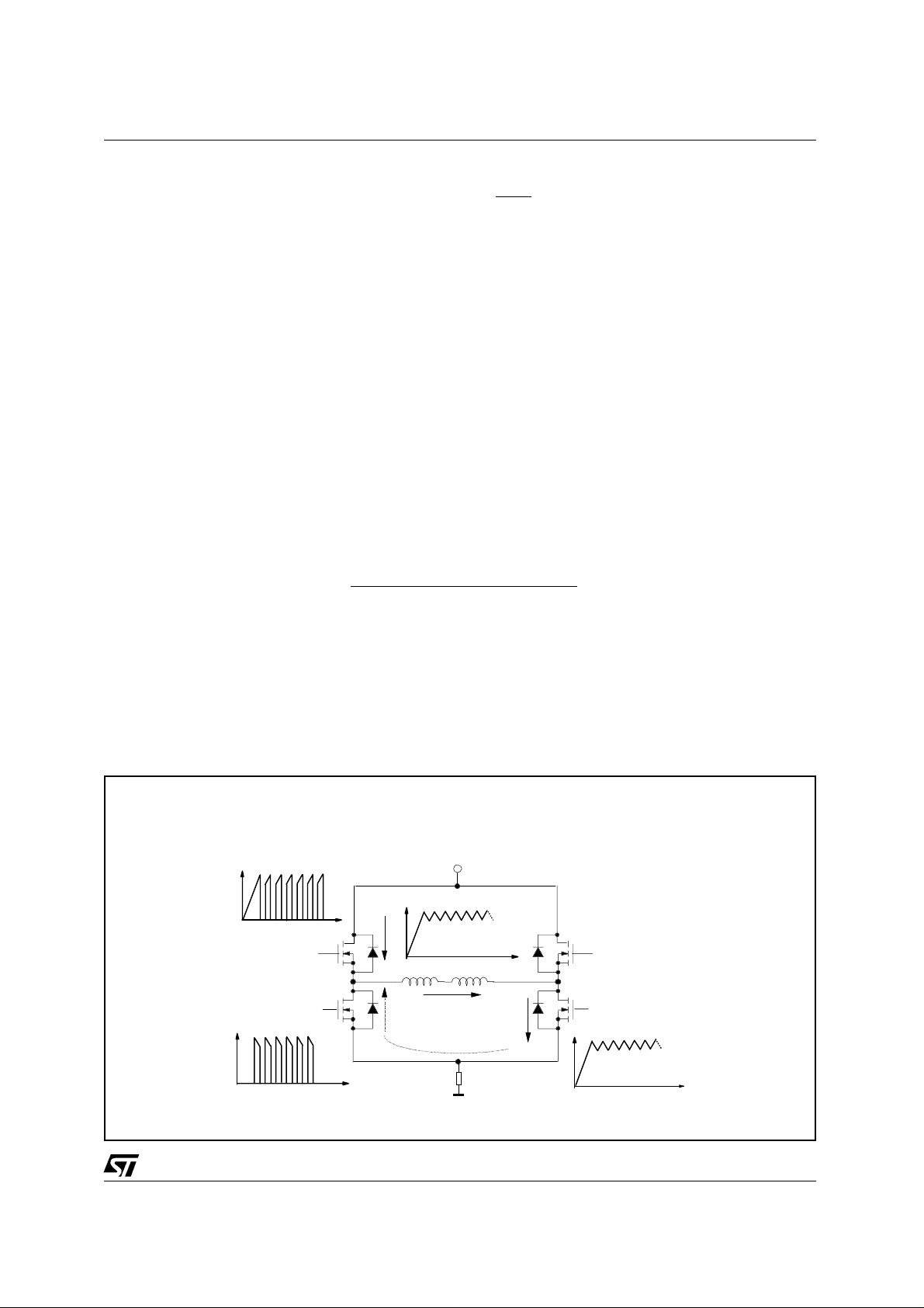
Figure 9. In put chopping curren t cir c ulation.
_
PHASE 12
CHOPPING INPUT
Vs
ILOAD
ILOAD
I1B
IOFF
half bri dge 2
I2B
OFF
ON
I2B
I1B
I1A
half bri dge 1
I1A
ON/OFF
OUT1 OUT2
OFF/ON
5/14
Page 6

AN1088 APPLICATION NOTE
Figure 10. Three Phase Brushless motor control sequence.
IOUT1
BRUSHLESS MOTOR
OUT1
OUT2
L6234
OUT3
IOUT2
IOUT3
T
The device soldered on the copper heat dissipating
area on the board ,without any additional heat sink,
can sustain a DC load current of 2.3 A at T
amb
approximately 40 °C.
The board provides a closed loop speed and torque
control, with a constant TOFF chopping current control method. It allows the user to change the direction and brake the motor.
Constant t
Chopping Current Control.
OFF
Figure 11. L6234 Power Dissipation in Three
of
Pd [W]
Phase Brushless Motor Control.
INPUT CHOPPING
Vs=36V
15
L=2mH
T=2ms
Tj=100C
10
fchop=50 k Hz
fchop=30 k Hz
DC
When the current through the motor exceeds the
threshold, fixed by the ratio between the control
voltage Vcontrol and the sensing resistor, Rsense,
5
an error signal is generated, the output of the
LM393 comparator switches to ground. This state is
maintained by the monostable (M74HC123) for a
constant delay time ( t
) generating a PWM sig-
OFF
nal that achieves the chopping current control. The
PWM signal is used for chopping the INPUT pat-
0
01
2
ILOAD [A ]
3
45
tern. During the toff in chopping current control, the
current flows in the low side loop ( see fig. 9 ) and does not flow through the sensing resistor.
The t
A suitable value of toff for the majority of applications is 30µs. The larger the t
rent ripple. If t he t
value can be set by the R9 and C11 to values shown in the table 1.
OFF
is too large the ripple current becomes excessive . On the other hand if the t
OFF
, the higher is the cur-
OFF
OFF
is
too small the winding current cannot decrease under the threshold and current regulation is not guaranteed.
6/14
Page 7

Figure 12. Application board Schematic Circuit.
AN1088 APPLICATION NOTE
+5V
HALL
EFFECT
SIGNALS
BRAKE
DIR
PWM
OUT
C7
10uF
3
PWM
L7805
2
GND
CONTROL
LOGIC
1
C6
220nF
CONSTANT toff
T1
IN
Z1
18V
IN1
IN2
IN3
EN1
EN2
EN3
CHOPPING
10k
R5
J7
CURRENT
CONTROL
Figure 13. Constant toff current control.
+5V
+5V
C9
100nF
1
LM393
4
PWM
+5V
C10
100nF
+5V
Vcontrol
_
Q
R9
100k
2316
M74HC123
monostable
4
15
B
14 8
C11
330pF
R11
10k
1
A
100uF
60V
Vsense
Vcontrol
8
+
Vs=8V to 42
C1
R1010K each
2
3
R8
1K
IN1
IN2
IN3
EN1
EN2
EN3
TORQUE &
1K
R6
C8
470pF
R7
11 k
C2
100nF
7
4
14
8
3
13
GND
+5V
SPEED
CONTRO L
Vsense
+5V
J1
1N4148 1N4148
D1 D2
912 17
L6234
POWER SO20
1
10 11 20
Vref
Table 1. toff selection
C3
10nF
18
16 19
C5
1uF
Hall effect signal
Reference
Speed
C4
220nF
VbootVcpVs
OUT1
6
OUT2
5
OUT3
15
2
SENSE
R1
Ω
1
BRUSHLESS MOTOR
R2 R3
Ω
1
Ω
1
REFERENCE
SPEED
1
toff R9 C11
20µs 100k 270pF
30µs 100k 330pF
45µs 100k 560pF
70µs 100k 1nF
HALL
EFFECT
SENSORS
R4
Ω
Torque & Speed Clos e d Loop C ontrol.
The motor’s rotational speed is determined by the frequency of the Hall effect signals. The speed control
loop has been achieved by comparing this f requency with a frequ ency of a reference os cillator (see f ig.
14) that corresponds to a desired speed limit.
Figure 14. PLL Motor Control.
REFERENCE
FEEDBACK
PHASE/
FREQUENCY
DETECTOR
Vcontrol
Amp.
COMPENSATION
NETWORK
D01IN1209
PWM
MOTOR
HALL
SENSORS
7/14
Page 8

AN1088 APPLICATION NOTE
Figure 15. Oscillator for Reference Speed.
Reference Speed
+5V
R26
C21
36K
8
3
NE555
1
R27
4
7
16K
6
2
5
C20
100nF
C19
100nF
100nF
Figure 16. Phase Locked Loop and filtering.
+5V
C12
100nF
Vcontrol
+5V
GND
HALL1 (Speed feedback)
Reference Speed
LM358
8
+
-
1
4
R12
47K
R14
47K
3
2
1uF
C13
R13
47K
+5V
BAT47
+5V
R15
P2
47K
1K
P1
5K
C14
100nF
+5V
R17
10M
R18
33K
R16
270K
810
9
Loop
Amplifier
+VIN
13
Phase/ Frequency
14
6
Figure 17. Control Logic Circ uit.
+5V
R29
10k
2
3
4
5
6
100nF
SW2
7
191
18
GAL 16V8
C18
17
16
15
14
10
20
DIRECTION CHANGE
DIR =0 GND : BACK ROTATION
DIR = 5V : FORWARD ROTATION
BRAKE FUNCTION
BRAKE = GND : BRAKE
BRAKE = 5V : GO
MOTOR
HALL
EFFECT
SIGNALS
+5V
GND
+5V
R22
10k
BRAKE DIR
R23
10k
R25
10k
SW1
R24
10k
HALL1
HALL2
HALL3
BRAKE
R26
10k
J1
DIR
PWM
100nF
R20
Aux.
OP-AMP
2.5V
Detector
EN1
EN2
EN3
IN1
IN2
IN3
C15
11
3635
2
TP8
C17
47nF
3
C16
220nF
12
R19
91K
15
EN1
EN2
EN3
IN1
IN2
IN3
PWM
When the hall effect signal frequency is lower than the reference
frequency, the control voltage is
maintained to a value that set s the
motor current limit and therefore the
torque control limit. The peak current limit is given by Ipeak = Vcontrol/Rsense.
When the frequency from the Hall
Effect sensors exceeds the reference frequency and an error signal
is generated by the PLL (see Fig.
14). An LM358 comparator, a loop
amplifier and an auxiliary OP-AMP
ensure the right gain and filtering to
guarantee the stability (see fig.16).
The error signal causes Vcontrol
decrease to a value that sets the
PWM chopping current control in order to reduce the torque and set
the desired speed. The motor
speed is regulated to within ± 0.02
% of the desired speed.
R21
91K
Output
4
Control Logic Ci r c uit.
The logic sequence to the motor is
generated by a GAL16V8, which
decodes the Hall Effect signals and
5
7
1
16
GND
generates the INPUT and ENABLE
pattern shown in Fig. 18.
The brake function is obtained by
setting the input pattern to logic low
and thus turning on the lower
DMOS switches of the enabled halfbridges.
The PWM signal is used for chopping the INPUT pattern.
The control logic circuit decodes
Hall effect sensors having different
phasing.
With the DIR jumper opened the
application achieves forward rotation for motors having 60° and 120°
Hall Effect sensor electrical phasing
and the reverse rotation for motors
having 300° and 240° Hall Effect
sensor phasing.
Connecting the DIR jumper to
ground sets the reverse rotation for
motors having 60° and 120° Hall
sensors phasing and the forward
rotation for motors having 300° and
240° Hall sensor phasing.
The SW2 switch performs the startstop function.
8/14
Page 9

Figure 17.
AN1088 APPLICATION NOTE
SENSOR
SIGNALS
ENABLE
FORWARD
ROTATION
HALL1
HALL2
HALL3
EN1
EN2
EN3
IN1
IN2
IN3
0˚
ELECTRICAL DEGREES
360˚
REVERSE
ROTATION
MOTOR
DRIVE
CURRENT
IN
FORWARD
ROTATION
IN1
IN2
IN3
IOUT1
IOUT2
IOUT3
0
0
0
NO PWM PWM CONSTANT t
OFF
D98IN912
9/14
Page 10

AN1088 APPLICATION NOTE
Layout Considerations.
Special attention must be taken to avoid overvoltages at Vs and additional negative voltages to the
SENSE pins and noise due to distributed inductance. Thus the input capacitor must be connected close
to the Vs pins with symmetrical paths. The paths between the SENSE pins and the input capacitor
ground have to be minimized and symmetrical . The sensing resistors must be non-inductive. The device GND has to be connected with a separate path to the input capacitor ground.
Figure 19. Application Board Layout.
Figure 20. Com pone nt side.
10/14
Page 11

AN1088 APPLICATION NOTE
Figure 21. Coppe r s ide.
APPLICATION ID EAS.
The L6234 can be used in many different applications. Typical examples are a half bridge driver using
one channel and a full bridge driver using two channels. In addition, the bridges can be paralleled to reduce the RDSon and the device dissipation.
The paralleled configuration can also be used to increase output current capability. Channel 1 can be
paralleled with Channel 3 or Channel 2 can be paralleled with Channel 3. Channel 1 should not be paralleled with Channel 2 because the sources of their low side DMOSs are connected to the same SENSE1
pin .
Application ideas for the L6234 follow.
Figure 22. Constant frequency current control
Vs
EN1
+5V
EN2
EN3
IN1
IN2
IN3
Reset
Q
S
R
S
R
Q
OSC
Rx
Cx
+5V
100nF
L6506
Vsense
Vcontrol
CONTROL
LOG IC
100uF
EN1
EN2
EN3
IN1
IN2
IN3
Constant frequency
+5V
Curren t Co n t ro l
1
Fchop= __________
0.69 Rx Cx
for Rx>10kOhm
100nF
GND
1N4148 1N4148
10nF
Vs
L6234
POWER SO20
Vref
SENSE1
1uF
220nF
VbootVcp
OUT1
OUT2
OUT3
SENSE2
RSENSE
11/14
Page 12

AN1088 APPLICATION NOTE
Low Cost Application with Speed and Torque Control Loops.
Figure 23. Complete three phase brushless motor application with speed and torque control.
V
S
HALL
EFFECT
BRUSHLESS MOTOR
V5
Vm
2
R1 100K
3
Vref
(Reference
SENSORS
+5V
1/fe
Ton
1Q
Rx1
100K
SPEED LOOP
163
1/2
M74HC123
MONOSTABLE
13
15 1 14 8
Cx1
V5=+5V
27
1B
HALL EFFECT SIGNAL
HALL
EFFECT
SIGNALS
PWM
+5V
V5=+5V
Q
Rx2
CONTROL
LOGIC
1/2
M74HC123
MONOSTABLE
12
IN1
IN2
IN3
EN1
EN2
EN3
1110
1
6
Cx2
912
L6234
POWER SO20
V
SENSE
6
5
+
17 18
16 2 19
R3 4KVCONTROL
R4
1K
7
4
14
8
3
13
1,10,11,20
GND SENSE
+5V
A
7
11
1/4
TSM221
D01IN1210
1/4
TSM221
6
5
15
C1 200nF
R2 1M
1
4
OUT1
OUT2
OUT3
R
SENSE
0.3W
+
Speed Voltage)
A low cost solution to obtain a complete three phase brushless motor control application with speed and
torque closed control loop is shown in Fig. 23. This simple low cost solution is useful when high dynamic
performances and accuracy of the speed loop are not required.
The current regulation limit, which determines the torque , is given by Vcontrol/Rsense. The constant
toff of the PWM is fixed by Rx2 and Cx2.
The speed loop is realised using a Hall effect signal, whose frequency is proportional to the motor
speed. At each positive transition of the Hall effect sensors the monostable maintains the pulse for a
constant time , Ton, with a fixed amplitude, V5. The average value of this signal is proportional to the frequency of the Hall effect signal and the motor speed . An OP-AMP configured as an integrator , filters
this signal and compares it with a reference voltage, Vref, which sets the speed . The generated error
signal is the control voltage, Vcontrol, of the currrent loop. Therefore the current loop modifies the produced torque in order to regulate the speed at the desired value.
The values of Cf and R2 should be chosen to obtain a nearly ripple free op-amp output, even at low motor speed. This constrain limits the system bandwidth and so limits the response time of the loop.
The regulated speed, for a rotor with n pairs of permanent magnetic poles , is given by :
R1
1 +
ωm =
V5 ⋅ Ton ⋅ n +
with KG =
R2
⋅ Vref ⋅ 60 [RPM]
1
KG
R4
R3 + R4
⋅ Kt ⋅
1
Rsense
⋅
1
B
R2
⋅
R1
in which Kt, expressed in [Nm/A] , is the Motor Torque constant and B, expressed in [Nms], is the Total
Viscous Friction.
In most cases 1/KG can be neglected.
12/14
Page 13

AN1088 APPLICATION NOTE
The Ton values, given by KCx1Rx1, must be less than the period of the Hall effect electrical signal at
the desired motor speed , so Ton must meet the requirement of 1.1 :
( 1.1 ) Ton <
For the motor and the load used in this application, which have the following parameters :
-4
Jt = 10
[Kg ⋅ m2] (Motor plus Load Inertia Moment); Kt = 10-2 [Nm/A] ; B = 10-5 [Nms]
n=4 ; R1=100k +/- 10% [kΩ] ; R2=1M ±1[kW] ; Cf=220n [F]
A regulated speed of 6000RPM can be obtained with an accuracy of around +/-3%, considering Ton accuracy of +/-1% , the V5 and Vref mismatch of +/-1% .
If the speed is 6000RPM, there are 100 rotor revolution for second, with n=4, the Hall effect frequency
is 400Hz. Therefore Ton has to be lower than 2.5ms (according to equation 1.1).
The phase margin is about 45° and the response time of the speed loop for a speed step variation is
around 200ms .
6X6 BRUSHLESS APPLICATION
Figure 24. 6x6 Three Phase Brushlees Application Circuit
60
n ⋅ ωm
SPEED AND POSITION
FEEDBACK
CONTROL
LOGIC
Constant Toff PWM
Current Control. Two M74HC124 plus an LM339
Compara tor & monostable
+5V
100nF
1
A
15
PWM3
+5V
100nF
_
4
Q
16
23
M74HC123
monostable
14 8
B
1
+5V
+5V
8
+
4
IN1A
IN1B
IN2A
EN1
IN3A
IN3B
IN2B
EN3
LM339
EN2
1K
470pF
Vs
100uF
Vs
100uF
Vsense3
Vcontrol
100nF
IN1
IN2
IN3
EN1
EN2
EN3
100nF
IN1
IN2
IN3
EN1
EN2
EN3
1N4148
Vs
GND
1N4148
Vs
GND
1N4148
10nF
Vcp
L6234
Vref
Vcp
L6234
Vref
Vboot
SENSE2
1uF
1N4148
10nF
OUT1
OUT2
OUT3
SENSE1
Vboot
OUT1
OUT2
OUT3
SENSE1
SENSE2
1uF
220nF
220nF
OUT1A
OUT1B
OUT2A
OUT2B
OUT3A
OUT3B
THREE PHASE
BRUSHLESS
MOTOR
PWM2
PWM1
Compar ator & monostable
Compara tor & monostable
Vsense2
Vsense1
13/14
Page 14

AN1088 APPLICATION NOTE
Information furnished is believ ed to be accurate and reliable. How ever, STMicroelect ronics assumes no responsibility for the consequences
of use of such informati on nor for any infringement of patents or other ri ghts of third parties which may result from its use. No license is
granted by implication or otherw ise under any patent or patent rights of STMic roelectronics . Specification mentioned in this publication are
subject to c hange without notice. Thi s publication supersedes and replac es all information previously su ppl ie d. S TMicroelectronics products
are not authorized for use as critical components in life support devices or systems without express written approval of STMicroelectronics.
The ST logo is a registered trademark of STMicroelect roni cs
© 2001 STMicroelectronics – Printed in Italy – All Rights Reserved
STMicroelectronics GROUP OF COMPANIES
Australia - Brazil - China - Finland - France - Germany - Hong Kong - India - Italy - Japan - Malaysia - Malta - Morocco -
Singapore - Spain - Sweden - Switzerland - United Kingdom - U.S.A.
http://www.st.co m
14/14
 Loading...