

Page 1
AN1061
APPLICATION NOTE
DESIGNING WITH L4978,
2A HIGH EFFICIENCY DC-DC CONVERTERY
1 INTRODUCTION
The L4978 is a 2A monolithic dc-dc converter, step- down , operating at fix frequency continuous mode.
It is realised in BCD60 II technology, and it’s available in two plastic packages, MINIDIP and
SO16L.
One direct fixed output voltage at 3.3V ±1% is available, adjustable for higher output voltage
values, till 40V, by an external voltage divider.
The operating input supply voltage ranges from 8V to 55V, while the absolute value, with no
load, is 60V.
New internal design solutions and superior technology performance allow to generate a device
with improved efficiency in all the operating conditions and with reduced EMI due to an innovative internal driving circuit, and reduced external component counts.
While internal limiting current and thermal shutdown are today considered standard protection
functions, mandatory for a safe load supply, oscillator with voltage feedforward improves line
regulation and overall control loop.
Soft-start avoids output overvoltages at turn-on, while, shorting this pin to ground, the device
is completely disabled, going into zero consumption state.
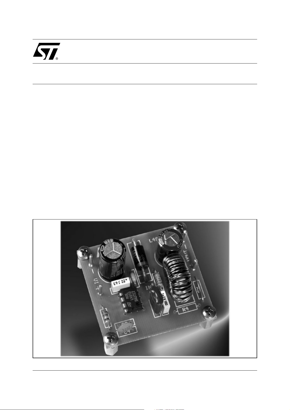
Figure 1.
AN1061/0505
Rev. 9
1/21
Page 2
AN1061 APPLICATION NOTE
2 DEVICE DESCRIPTION
For a better understanding of the device and its working principles, a short description of the
main building blocks is given here below, with packaging options and complete block diagram.
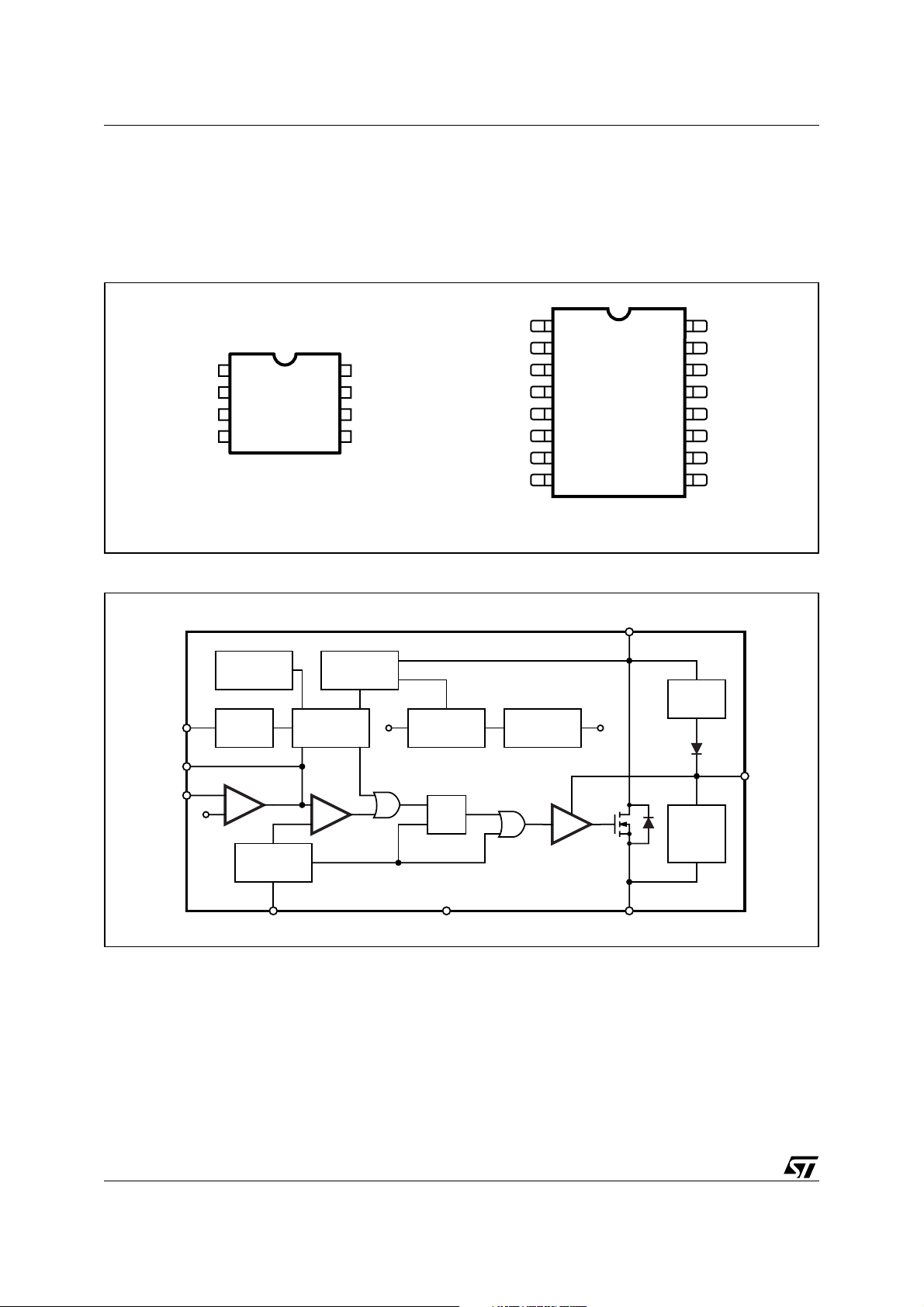
Figure 1 shows the two packaging options, with the pin function assignments.
Figure 2. Pins Connection.
GND
SS_INH
OSC
OUT
1
2
3
4 VCC
D97IN595
Figure 3. Block Diagram
THERMAL
SHUTDOWN
FB
2
INHIBIT SOFTSTART
7
8
3.3V
E/A
OSCILLATOR
SS_INH
COMP
7
6
5
VOLTAGES
MONITOR
PWM
FB8
COMP
BOOT
3.3V
INTERNAL
REFERENCE
R
Q
S
N.C.
SUPPLY
2
3
4
5
6
7
8
D97IN596
5.1V
DRIVE
GND
SS_INH
OSC
OUT
OUT
N.C.
N.C. N.C.
INTERNAL
16
15
14
13
12
11
10
9
VCC
5
CBOOT
CHARGE
CBOOT
CHARGE
AT LIGHT
LOADS
N.C.1
N.C.
FB
COMP
BOOT
VCC
N.C.
6
BOOT
3
OSC GND OUT
1
4
D97IN594
3 POWER SUPPLY & VOLTAGE REFERENCE
The device is provided with an internal stabilised power supply (of about 12V typ. ) that powers
the analog and digital control blocks and the bootstrap section.
From this preregulator, a 3.3V reference voltage ±2%, is internally available.
Oscillator and voltage feedforward.
Just one pin is necessary to implement the oscillator function, with inherent voltage feedfor-
ward.
2/21
Page 3
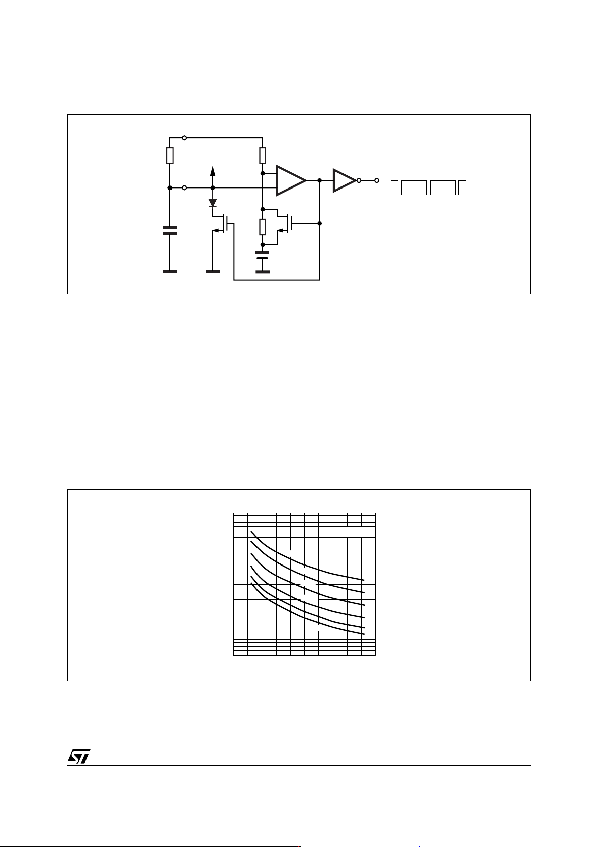
Figure 4. Oscillator Internal Circuit.
V
CC
AN1061 APPLICATION NOTE
R
OSC
C
OSC
TO PWM
COMPARATOR
Osc
Q
1
5R
-
+
Q
R
2
1V
CLOCK
D97IN655A
A resistor Rosc and a capacitor Cosc connected as shown in Figure 4, allow the setting of the
desired switching frequency in agreement with the below formula:
1
6
-- -
5
100 C
⋅+
osc
Where F
is in kHz, R
sw
in KΩ and C
osc
SW
--------------------------------------------------------------------------------------=
R
oascCosc
in nF.
osc
⋅()In
The oscillator capacitor, Cosc, is discharged by an internal mos transistor with 100W of Rdson
(Q1) and during this period the internal threshold is set at 1V by a second mos, Q2 . When the
oscillator voltage capacitor reaches the 1V threshold, the output comparator turns off the mos
Q1 and turns on the mos Q2, restarting the Cosc charge.
The oscillator block, shown in figure 5, generates a sawtooth wave signal that sets the switching frequency of the system.
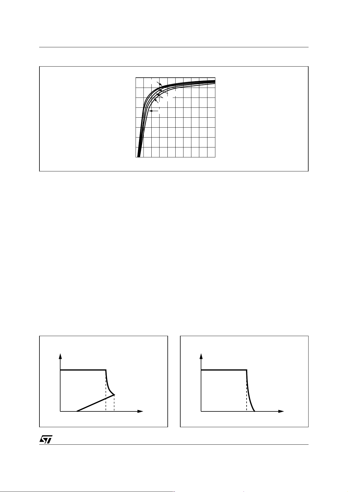
Figure 5. Switching frequency vs. Rosc and Cosc.
fsw
(KHz)
500
200
100
50
20
10
5
0 20 40 60 80 R2(KΩ)
0.82nF
1.2nF
2.2nF
3.3nF
5.6nF
D97IN630
Tamb=25˚C
4.7nF
This signal, compared with the output of the error amplifier, generates the PWM signal that will
modulate the conduction time of the power output stage.
The way the oscillator has been integrated,does not require additional external components to
benefit of the voltage feedforward function.
3/21
Page 4
AN1061 APPLICATION NOTE
The oscillator peak-to-valley voltage is proportional to the supply voltage, and the voltage
feedforward is operative from 8V to 55V of input supply.
osc
VCC1–
--------------------=
6
∆V
Also the ∆V/∆t of the sawtooth is directly proportional to the supply voltage. As Vcc increases,
the Ton time of the power transistor decreases in such a way to provide to the chocke, and
finally also the load, the product Voltxsec constant.
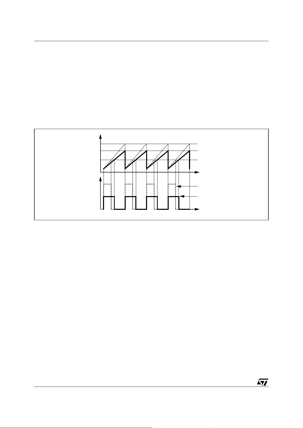
Figure 6 shows how the duty cycle varies as a result of the change on the ∆V/∆t of the sawtooth
with the Vcc.
Figure 6. Voltage Feedforward Function
V1
V2-3
D97IN684
Vi=30V
Vi=15V
Vc
t
Vi=30V
Vi=15V
t
The output of the error amplifier doesn’t change in order to maintain the output voltage constant and in regulation.
With this function on board, the output response time is greatly reduced in presence of an
abrupt change on the supply voltage, and the output ripple voltage at the mains frequency is
greatly reduced too.
In fact, the slope of the ramp is modulated by the input ripple voltage, generally present in the
order of some tens of Volt, for both off-line and dc-dc converters using mains transformers.
The charge and discharge time are approximable to:
6
In
-- -
5
T
ch
⋅⋅=
R
oscCosc
T
100 C
dis
⋅=
osc
The maximum duty cycle is a function of Tch, Tdis and an internal delay and is expressed by
the equation:
Dmax
R
oscCosc
----------------------------------------------------------------------------------=
R
oscCosc
In
In
6
-- -
5
6
-- -
5
100 C
80 10
⋅–⋅⋅
⋅+⋅⋅
9–
osc
and is represented in figure 7.
4/21
Page 5
AN1061 APPLICATION NOTE
Figure 7. Maximum Duty Cycle vs Rosc and Cosc as Parameter
D
max
0.90
0.80
0.70
0.60
5.3nF
4.7nF
2.2nF
1.2nF
0.8nF
0 4 8 121620242832R
D97IN685
OSC
(KΩ)
3.1 Current Protection
The L4978 has two current limit levels, pulse by pulse and hiccup modes.
Increasing the output current till the pulse by pulse limiting current threshold (Ith1 typ. value of
3A) the controller reduces the on-time till the value of TB = 300ns that is a blanking time in
which the current limit protection does not trigger. This minimun time is necessary to avoid undesirable intervention of the protection due to the spike current generated during the recovery
time of the freewheeling diode.
In this condition, because of this fixed balnking time, the output current is given by:
I
max
----------------------------------------------------------------------------------------------------------------------------------------------------=
R
ORDRL
VCCTBF
SWVf
+()1TBFSW⋅–()R
1TBFSW⋅–()⋅–⋅⋅[]
+()TBFSW⋅++[]
dsonRL
Where Ro is the load resistance, Vf is the diode forward voltage. RD and RL are the series
resistance of,
respectively, the freewheeling diode and the choke.
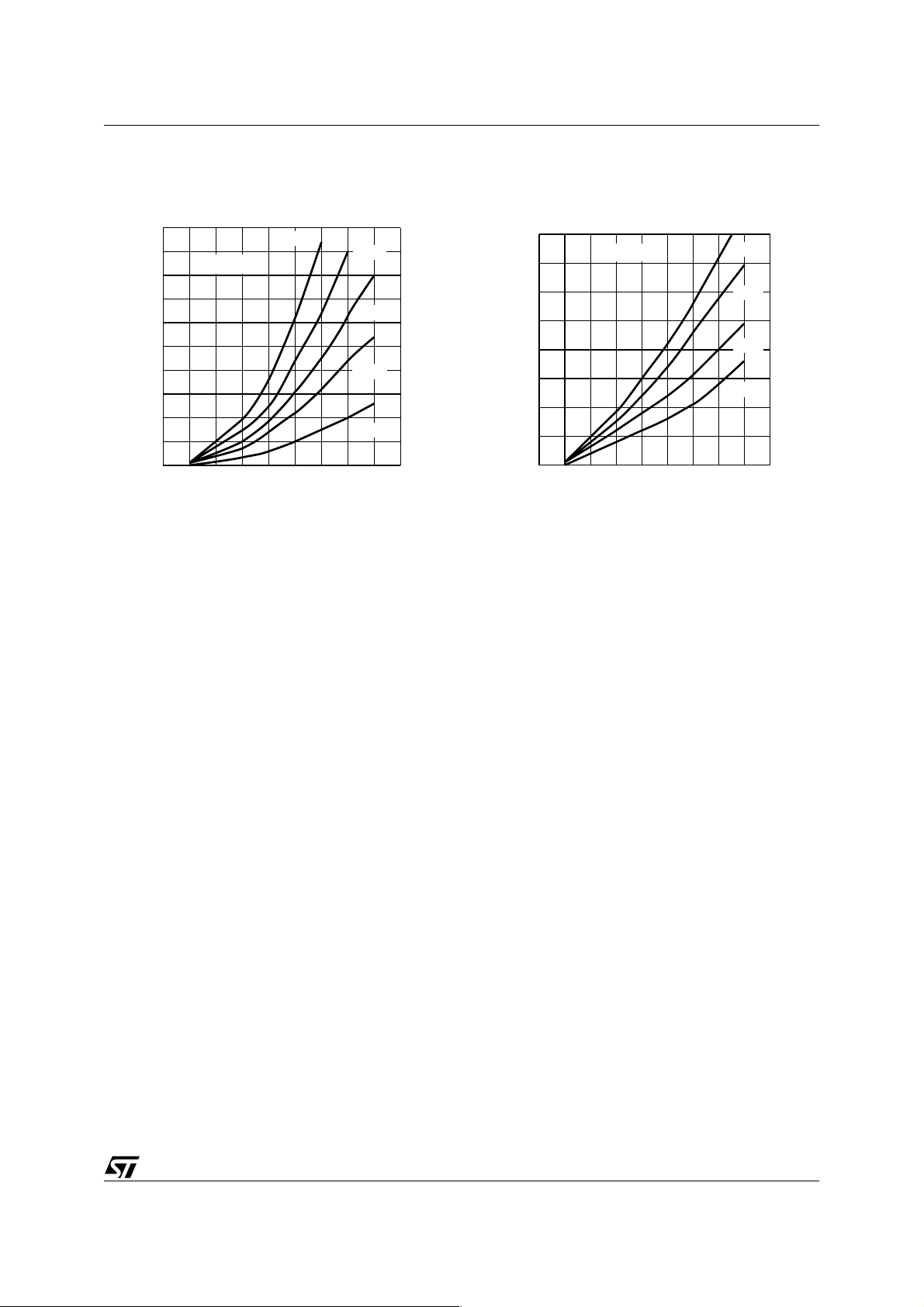
Typical output characteristics are represented in figure 8 and 9.
In fig 8, the pulse by pulse protection is sufficient to limit the current.
In fig 9 the pulse by pulse protection is no more effective to limit the current due to the minimun
Ton fixed by the blanking time TB, and the hiccup protection intervenes because the output
peak current reachs the relative threshold.
Figure 8. Output Characteristic Figure 9. Output Characteristic
V
O
D98IN909A
A
B
C
3.6A
3A
I
O
V
O
D99IN1077
3A
A
I
3.6A
O
5/21
Page 6
AN1061 APPLICATION NOTE
At the pulse by pulse intervention (point A) the output voltage drops because of the Ton reduction, and the current is almost constant. Going versus the short circuit condition, the current is
only limited by the series resistances RD and RL (see relation above) and could reach the hiccup threshold (point B), set 20% higher than the pulse by pulse. Once the hiccup limiting current is operating, in output short circuit
condition, the delivered average output current
decreases dramatically at very low values (point C).
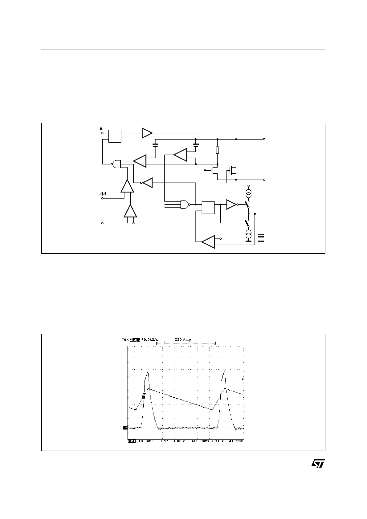
Figure 10. Current Limit internal schematic circuit.
Q
S
OSC
R
V
Th1
+
-
V
Th2
+
-
V
CC
12V
OUT
C
SS
OSC
VFB
PWM
+-
VREF
+-
HICCUP
THERMAL
UNDERVOLTAGE
D97IN658
SOFT START
LATCH
Q
S
R
+
-
0.4
Figure 10 shows the internal current limiting circuitry. Vth1 is the pulse by pulse while Vth2 is
the hiccup threshold.
The sense resistor is in series with a small mos realised as a partition of the main DMOS.
The Vth2 comparator (20% higher than Vth1) sets the soft start latch, initialising the discharge
of the soft start capacitor with a constant current (about 22µA). Reaching about 0.4V, the valley
comparator resets the soft start latch, restarting a new recharge cycle.
Figure 11 Shows the typical waveforms of the current in the output inductor and the soft start
voltage (pin 2).
Figure 11. Output current and soft-start voltage
6/21
Page 7
AN1061 APPLICATION NOTE
Figure 12. Maximum Soft Start
Capacitance with f
L
(µH)
fsw=100KHz
400
300
200
100
0
15 20 25 30 35 40 45 50 V
680nF
SW
= 100kHz
D97IN745
470nF
330nF
220nF
100nF
(V)
CCmax
Figure 13. Maximum Soft Start
Capacitance with fSW = 200kHz
L
(µH)
300
200
100
0
15 20 25 30 35 40 45 50 VCCmax(V)
fsw=200KHz
D97IN746
56nF
47nF
33nF
22nF
During the recharging of the soft start capacitor, the Ton increases gradually and, if the short
circuit is still present, when Ton>T
and the output peak current reachs the threshold, the hic-
B
cup protection intervenes again. So, the value of the soft start capacitor must not be too high
(in this case the Ton increases slowly thus taking much time to reach the T
value) to avoid
B
that during the soft start slope the current exceeds the limit before the protection activation.
The folllowing diagrams of Figure 12 and Figure 13 show the maximum allowed soft-start ca-
pacitor as a function of the input voltage, inductor value and switching frequency. A minimun
value of the soft start capacitance is necessary to guarantee, in short circuit condition, the
functionality of the limiting current circuitry. Infact, with a capacitor too small, the frequency of
the current peaks (see figure 11) is high and the mean current value in short circuit increases.
3.2 Soft Start and Inhibit functions.
The soft start and the inhibit functions are realised using one pin only, pin2. Soft-start is requested to inizialise all internal functions with a correct start-up of the system without overstressing the power stage, avoiding the intervention of the current protection, and having an
output voltage rising smoothly without output overshoots.
At Vcc Turn-on or having had an intervention of inhibit function, an initial 5µA internal current
generator starts to charge the soft-start capacitor, from 0V to about 1.8V. From this hysteretic
threshold, a 40µA current generator is activated, putting in off state the previous generator.
At this point, the output PWM starts, initiating the rising phase of the output voltage.
The soft-start capacitor is quickly discharged in case of:
■ Thermal protection intervention
■ Hiccup limiting current condition
■ Supply voltage lower than UVLO off threshold.
The soft-start and inhibit schematic diagram is shown in figure 14.
7/21
Page 8

AN1061 APPLICATION NOTE
Figure 14. Soft-Start and inhibit functions Internal Circuit .
12V
UNDERVOLTAGE PROT.
HICCUP PROT.
THERMAL PROT.
S
R
Q
Comp2
+
-
1.3V
40µA
S1
S2
10µA
5µA
S4
S3
Comp1
+
-
1.2V 1.8V
SS_INH
1KΩ
C
D97IN808A
SS
At device turn-on, the soft-start capacitor has no charge, with 0V at its terminals.
From 0V to 1.8V, switch S3 is opened and S4 is closed.
Soft-start capacitor is charged with 5µA.
At 1.8V, comp1 change the output status, opening S4 and closing S3, and the device starts to
generate the PWM signal, rising smothly the output voltage.
Till this moment, S2 is opened, S1 closed.
By closing S3, the soft-start capacitor is charged with 40mA reaching its saturation voltage.
This procedure is repeated at each Vcc turn-on.
Turning Vcc off, the soft-start capacitor is discharged with a constant 10µA (S2 closed, S3
closed, S1 and S4 open), from the moment when Vcc is crossing the UVLO off threshold.
The final discharge value is 1.2V.
In case of the Css is discharged using an external grounded element when the voltage at Css
reaches the threshold of 1.3V Comp2 resets the flip flop, S1 is closed, S2 is opened and the
40µA current generator is activated. The external switch, sinking some mA, discharges the
soft-start under the 1.2V Comp1 threshold, opening S3 and closing S4. At this point the device
is in disable, sourcing only 5µA through pin 2.
When the external grounding element is removed, the device restarts charging the soft start
capacitance, initially, with 5µA till the voltage reaches the 1.8V threshold and Comp1 connects
the 40µA charging current generator.
In case of thermal shutdown or overcurrent protection intervention the power is turned off and
the flip flop turns off S2 and turns on S1. The soft-start is discharged till the voltage reaches
the 1.3V threshold, and Comp2 resets the flip flop. S1 is closed, S2 is opened and the softstart capacitance is charged again.
Figure 15 shows the systems signals during Inhibit, overcurrent and Vcc turn off.
t1 and t2 can be calculated by the following equations:
V
O
t1 0.36 Css;⋅= t2
----------------------------------- C
Ich6D
⋅⋅
max
⋅=
ss
where Dmax is 0.95, Css is in µF and Ich is in µA .
Soft-start time (t2) versus output voltage and Css is shown in Figure 17.
Thanks to the voltage feedforward, the start-up time (t2) is not affected by the input voltage.
Figure 18 shows the output voltage start-up using different soft-start capacitance values.
It is mandatory a minimum capacitor value of 22nF. The pin 2 cannot be left open.
8/21
Page 9

AN1061 APPLICATION NOTE
Figure 15. Timing Diagram in Inhibit, overcurrent and turn off condition
INHIBIT OVER-CURRENT TURN-OFF
V
SS/INH
1.8V
1.3V
1.2V
I
C
PWM
V
O
I
I
LIM
I
O
LIM
t
t
t
t
V
CC
Figure 16. Start up sequence.
V
V
CC
UVLO
ON
SS/INH
1.8V
I
PWM
UVLO
D97IN811
OFF
t
t
t
1
C
t
t
V
O
t
2
D97IN812
t
9/21
Page 10

AN1061 APPLICATION NOTE
3.3 Feedback Disconnection
In case of feedback disconnection, the duty cycle increases versus the max allowed value
bringing the output voltage close to the input supply. This condition could destroy the load.
To avoid this dangerous condition, the device is forcing a little current(1.4µA typical) out of the
pin 8 (E/A Feedback). If the feedback is disconnected, open loop, and the impedance at pin 8
is higher than 3.5MΩ, the voltage at this pin goes higher than the internal reference voltage
located on the non-inverting error amplifier input , and turns-off the power device.
Figure 17. Soft start time(t2) vs Vo and
Css
Figure 18. Output rising voltage with Css
56nF, 100nF, 220nF.
t
ss
(ms)
70
60
50
40
30
20
10
0
0 3 6 9 12 15 18 21 24 VO(V)
D97IN687
1µF
470nF
330nF
220nF
100nF
3.4 Zero load
In normal operation, the output regulation is also guaranteed because the bootstrap capacitor
is recharged, cycle by cycle, by means of the energy flowing into the chocke.
Under light load conditions, this topology tends to operate in burst mode, with random repetition rate of the bursts.
An internal new function makes this device capable of keeping the output voltage in full regulation with 1mA of load current only.
Between 1mA and 500µA, the output is kept in regulation up to 8% above the nominal value.
Here the circuitry providing the control:
■ 1- a comparator located on the bootstrap section is sensing the bootstrap voltage; when this
is lower than 5V, the internal power VDMOS is forced ON for one cycle and OFF for the
next..
■ 2- during this operation mode, i.e. 500µA of load current, the E/A control is lost. To avoid
output overvoltages, a comparator with one input connected to pin 8, and the second input
connected to a threshold 8% higher that nominal output, turns OFF the internal power device
the output is reaching that threshold. When the output current, or rather, the current flowing
into the choke, is lower than 500µA, that is also the consumption of the bootstrap section,
the output voltage starts to increase, approaching the supply voltage.
3.5 Output Overvoltage Protection (OVP)
The output overvoltage protection, OVP, is realised by using an internal comparator, which input is connected to pin 8, the feedback, that turns-off the power stage when the OVP threshold
10/21
Page 11

AN1061 APPLICATION NOTE
is reached. This threshold is typically 8% higher than the feedback voltage.
When a voltage divider is requested for adjusting the output voltage, the OVP intervention will
be set at:
Ra Rb+()
V
OVP
1.08 V
---------------------------⋅⋅=
fb
Rb
where Ra is the resistor connected to the output.
3.6 Power Stage
The power stage is realised by a N-channel D-mos transistor with a Vdss in excess of 60V and
typ. Rdson of 290mOhm (measured at the device pins).
To minimise the Rdson, means also to minimise the conduction losses. But also the switching
losses have to be taken into consideration, mainly for the two following reasons:
a- they are affecting the system efficiency and the device power dissipation
b- because they generate EMI.
3.7 TURN - ON
At turn-on of the power element, or better, the rise time of the current(di/dt) at turn-on is the
most critical parameter to compromise.
At a first approach, it looks that the faster it is the rise time and the lower are the turn-on losses.
It’s not completely true.
There is a limit, and it’s introduce by the recovery time of the recirculation diode. Above this
limit, about 100A/µsec, only drawbacks are obtained:
1- turn-on overcurrent is decreasing efficiency and system reliability
2- big EMI encreasing.
The L4978 has been developed with a special focus on this dynamic area.
An innovative and proprietary gate driver, with two different timings, has been introduced.
When the diode reverse voltage is reaching about 3V, the gate is sourced with low current (see
Figure19) to assure the complete recovery of the diode without generating unwanted extra
peak currents and noise.
After this threshold, the gate drive current is quickly increased, producing a fast rise time till
the peak current, so maintaining the efficiency very high.
3.8 TURN - OFF
The turn-off behaviour, is shown at Figure19. Figure 20 shows the details of the internal power
stage and driver, where at Q2 is demanded the turnoff of the power switch, S.
4 TYPICAL APPLICATION
Figure 21 shows the typical application circuit, where the input supply voltage, Vcc, can range
from 8 to 55V operating, and the output voltage adjustable from 3.3V to 40V.
The selected components, and in particular input and output capacitors, are able to sustain the
device voltage ratings, and the corresponding RMS currents.
4.1 Electrical Specification
Input Voltage range 8V-55V
Output Voltage 5.1V ±3% (Line, Load and Temperature)
11/21
Page 12

AN1061 APPLICATION NOTE
Output ripple 34mV
Output Current range 1mA-2A
Max Output Ripple current 20% Iomax
Current limit 3A
Switching frequency 100kHz
Target Efficiency 85%@2A Vin = 55V
92%@0.5A Vin = 12V
Main components description
Figure 19. Turn on and Turn off (pin 2, 3)
Figure 20. Power Stage Internal Circuit.
Q
3
I
2
Q
5
I
3
DELAY
12/21
I
1
Q
4
I
4
I
5
from PWM LATCH
C
SS
V
1
2
i
S
D97IN659
C
SS
S
RS
L
+
V
CD
O
-
Q
Q
Page 13

AN1061 APPLICATION NOTE
4.2 INPUT CAPACITOR
The input capacitors have to be able to support the max input operating voltage of the device
and the max rms input current.
Figure 21. Application Circuit
Vin=8V to 55V
R
1
20K
C
220µF
63V
C
1
C1=220µF/63V EKE
C2=2.7nF
C5=100nF
C6=100nF
C7=220nF/63V
C8=330µF/35V CG Sanyo
L1=126µH KoolMu 77120 - 55 Turns - 0.5mm
R1=20K
R2=9.1K
D1=STPS3L60U
7
220nF
C
2.7nF
2
C
5
100nF
5
3
2
C
22nF
8
L4978
4
1
7
R
2
9.1K
4
6
C
6
100nF
STPS3L60U
D98IN915
D1
L1
126µH
(77120)
C
330µF
8
VO=5.1V/2A
R
3
R
4
L4978
VO(V) R3(KΩ) R4(KΩ)
3.3
5.1
12
15
18
24
2.7
12
16
20
30
0
4.7
4.7
4.7
4.7
4.7
The input current is squared and the quality of these capacitors has to be very high to minimise
its power dissipation generated by the internal ESR, improving the system reliability.
Moreover, input capacitors are also affecting the system efficiency.
The max Irms current flowing through the input capacitors is:
2
2
⋅
I
rmsIO
D
2D
-------------- -–
D
------ -+⋅=
2
η
η
where h is the expected system efficiency, D is the duty cycle and Io the output dc current. This
function reaches the maximum value at D = 0.5 and the equivalent rms current is equal to Io/2.
The following diagram is the graphical representation of the above equation, with an estimated
efficiency of 85% at different output currents.
The maximum and minimum duty cycles are:
D
VOVf+
---------------------------- 0.66==D
max
V
+
inminVf
max
VOVf+
------------------------------ 0.1==
V
+
inmaxVf
This formula is not taking into account the power mos Rdson, considering negligible the inherent voltage drop, respect input and output voltages.
At full load, 2A and D = 0.5% the rms capacitor current to be sustained is of 1A.
The selected EKE 220µF/63V Roderstain is able to support this current.
13/21
Page 14

AN1061 APPLICATION NOTE
Figure 22. Efficiency vs Output Current Figure 23. Input Capacitance rms current
vs duty cycle
I
RMS
1
IO=2A
D98IN916
0.8
0.6
0.4
0.2
0
0.1 0.2 0.3 0.4 0.5 0.6 0.7 0.8 D
IO=1.5A
IO=1.2A
IO=1A
IO=0.5A
IO=0.2A
4.3 Inductor Selection
The inductor ripple current is fixed at 20% of Iomax and is 0.4A, the inductor needed is:
1D
–()
min
LVOVf+()
2
L . I
is 0.53 and the size core chose is 77120 (125µ) Magnetics KoolMµ material. At full load
O
-------------------------- - 126µ H=⋅=
∆I
⋅
Ofsw
Eq 1
the magnetising force is about 25 Oersted, so, in order to compensate a 30% reduction of inductance due to the DC current level, they are wiring 55 turns, which corresponds to 213µH of
inductance at light load.
It is possible to graficate the Eq 1 as a function of Vo and Vinmax at 100kHz and 200kHz (see
Figure 24 and 25).
These curves are useful to define the inductor value immediately.
Figure 24. Inductor needed as a function
of maximum input voltage and
output voltage at fsw=100kHz
14/21
L
O
(µH)
V
=
CCmax
250
200
150
100
18V
15V
50
0
0 4 8 12 16 20 24 28
24V
D98IN917
40V
35V
30V
32 0 4 8 12 16 20 24 28
V
(V)
O
Figure 25. Inductor needed as a function
of maximum input voltage and
output voltage at fsw=200kHz
L
(µH)
250
200
150
100
50
0
O
V
=
CCmax
15V
18V
24V
30V
32
D98IN918
40V
35V
V
(V)
O
Page 15

AN1061 APPLICATION NOTE
4.4 Core Losses
Core losses are proportional to the magnetic flux swing into the core material. To evaluate the
flux swing is used the following formula:
L ∆I
⋅
⋅⋅
OAle
O
4–
10
where A
B
∆
is the core cross section [m2].
le
------------------------------------- 477G a u s s==
N
The choosen core material family has an empirical equation to calculate the losses:
sw
1.5
VI180m W=⋅⋅=
Where Vl is the core volume in cm
P
∆B2f
I
3
, ∆B is expressed in KGauss and fsw in KHz. The core in-
creasing temperature is:
∆T
-----------
13.6
8.5° C==
0.833
P
I
4.5 Output Capacitor
The selection of Cout is driven by the output ripple voltage required, 1% of Vo. This is defined
by the output capacitance ESR and with the maximum ripple current (0.4A) the maximum ESR
is:
ESR
∆V
----------- -
∆I
0.051
O
-------------- - 127.5m Ω== =
0.4
O
The selected capacitance is 330µF/35V CG Sanyo with ESR = 86mΩ and the ripple voltage is
0.67% of Vo (34mV).
The drop due to a fast load variation of 1A produce an output drop of :
ESR . ∆Io = 86mV
that is the 1.6% of the output voltage.
Output capacitance has to support a load transient until the inductor current reaches the in-
creased current. The output drop during an output current variation is:
∆V
-------------------------------------------------------------------------- -=
O
2C
)
Where ∆Io is the current load variation (0.5A to 2A), D
is 5.1V and Lo is 126µH .
V
o
∆IO()2LO⋅
OVinminDmaxVO
–⋅()⋅⋅
max
Eq 2
is the maximum duty cycle (0.95),
Equation 2, normalised by Vo is represented in the following diagram( Figure 26) as a function
of the minimum input voltage.
These curves are represented for different output capacitor 220µF, 330µF, 2x330µF.
Compensation Network
The complete control loop block diagram is shown in Figure 27
The transfer functions described are:
Error amplifier and compensation block
15/21
Page 16

AN1061 APPLICATION NOTE
A
1sRcC
As()
---------------------------------------------------------------------------------------------------------------------------------------------------- -=
2
s
RoCoRcCcsRoCcRoCoRcCc⋅+⋅+⋅()1+⋅+⋅⋅⋅⋅
VO
⋅⋅+()⋅
Figure 26. Output drop (%) vs minimum input voltage
∆V
O
·100
V
O
(%)
5
4
3
c
D98IN919
2
1
0
C
is the parallel between the output capacitance and the external capacitance of the Error
o
Amplifier R
and Cc are the compensation values
c
220µF
330µF
2 x 330
µF
812 20 28 3640V
inmin
(V)16 24 32
Figure 27. Block diagram compensation loop
V
REF
+-
A(s) Vc/Vct LC
α
D97IN697
V
O
4.6 LC Filter
4.7 PWM Gain
A
os()
--------------------------------------------------------------------------------------------------------------------------------=
LC
1R
R
est
1
out
-----------+
R
L
V
CC
-----------
V
ct
esrCout
2
s
V
CC
-------------------- 6≈=
V
CC
s⋅⋅+
R
esrCout
L
s1+⋅+⋅⋅
------ -+⋅
R
L
6⋅
1–
where Vct is the peak to peak sawtooth oscillator.
4.8 Voltage Divider
Figure 28. Error Amplifier Compensation Circuit
Cc
16/21
Rogm
Rc
α
D97IN698
R4
----------------------=
R3 R4+
Co
Avo=gm·R
o
Page 17

The Error Amplifier basic characteristics are:
)
R
= 1.2MΩ, Avo = 57dB, CO = 220pF
o
Figure 29. Output Filter
AN1061 APPLICATION NOTE
L
Cout
Iout=2A
R
L
Resr
D98IN925
The poles and zeros value are:
o
2 πR
F
---------------------------------------
p
2 π LC
F
ocomp
F
----------------------------------
p1
2 π R
F
----------------------------------
p2
2 π R
⋅⋅
esrCout
1
⋅⋅⋅
out
1
--------------------------------- -
⋅⋅ ⋅
2 π R
1
⋅⋅ ⋅
oCc
1
⋅⋅ ⋅
cCo
1
---------------------------------------
F
------------------------------------------------------------- 5.6K H z== =
⋅⋅ ⋅ ⋅
2 π 0.086 330 10
----------------------------------------------------------------------------- 780H z== =
2 π 126 10
----------------------------------------------------------------- 795Hz== =
cCc
2 π 9.1 10
----------------------------------------------------------------- 6.032H z== =
⋅⋅ ⋅ ⋅ ⋅
2 π 1.2 10
----------------------------------------------------------------------- 80KHz== =
⋅⋅ ⋅ ⋅ ⋅
2 π 9.1 10
1
1
6–
330 10
⋅⋅⋅⋅⋅
1
3
⋅⋅ ⋅ ⋅ ⋅
22 10
1
6
22 10
1
3
220 10
6–
6–
9–
9–
12–
The compensation is realised choosing the Focomp nearly the frequency of the double pole
due to the LC filter. Using compensation network R1 = 9.1K, C6 = 22nF and C5 = 220pF obtain
the Gain and Phase Bode plot of Figures 24-25. Is possible to omit C5 because does not influence the system stability but is useful only to reduce the noise. The cut off frequency and a
phase margin are:
Fc = 3.7KHz; Phase margin = 21°
Figure 30. Gain Bode open loop plot Figure 31. Phase Bode open loop plot
Fa
(dB)
60
50
40
30
20
10
0
-10
-20
1 10 100 1K 10K f(Hz
D98IN920
φ
Fa
(˚)
-20
-40
-60
-80
-100
-120
-140
-160
-180
1 10 100 1K 10K f(Hz)
D98IN921
17/21
Page 18

AN1061 APPLICATION NOTE
5 APPLICATION IDEAS
5.1 Compensation of voltage drop along the wires.
For supplying a remote load, without using sensing wires, the below application shows how to
compensate the voltage drop along the wires.
If Rz is the total resistance of the line, fixing the resistor Rk, to a value given by the below formula :
R
Z
RkR
the regulated load voltage, VL , is :
,
-------⋅=
2
R
1
V
LRzIqR1R2
+()
1
------ - V
⋅⋅+⋅=
R
ref
2
where Vref is the feedback voltage reference of 3.3V and Iq is the device quiescent current
(typ. 2.5mA).
The Cadd capacitor has to be chosen so that the frequency, given by
1/[2πCadd·R1R2/(R1+R2)], is around two decades below the switching frequency.
It follows a table for Rk choice with, for example, a line resistance, Rz=0.5Ohm :
Figure 32. Compensation of Voltage Drop along the Wires
D98IN923
Iload
VL>3.3V
RL
VL
100nF
GND
L4978
I
q
BOOT
COMP
22nF
9.1K
OUT
FB
GI
SB560
126uH
(77120)
68nF
R1
VOUT
R2
100uF
Rk
Rz+jwLz
Vcc
20k
OSC
68nF
220uF
Vs
22uF
2.7nF
SS- INH
100nF
Table 1. Table for RK choice
Vload(V) R1(Ω)R2(Ω)Rk(Ω)
5.1 2.43K 4.7K 0.97
12 12.1K 4.7K 0.19
24 28.7K 4.7K 0.08
18/21
Page 19

Figure 33. Output Voltage vs. Output Current
[A]
AN1061 APPLICATION NOTE
V (V)
0
D98IN924
Vout
Rz Iout
VL
1
2
3
Iout
19/21
Page 20

AN1061 APPLICATION NOTE
6 REVISION HISTORY
Table 2. Revision History
Date Revision Description of Changes
September 2000 8 First Issue in EDOCS
May 2005 9 Updated the Layout look & feel.
Changed name of the D1 on the fig. 21
20/21
Page 21

AN1061 APPLICATION NOTE
The present note which is for guidance only, aims at providing customers with information regarding their products in
order for them to save time. As a result, STMicroelectronics shall not be held liable for any direct, indirect or
consequential damages with respect to any claims arising from the content of such a note and/or the use made by
customers of the information contained herein in connection with their products.
Information furnished is believed to be accurate and reliable. However, STMicroelectronics assumes no responsibility for the consequences
of use of such information nor for any infringement of patents or other rights of third parties which may result from its use. No license is granted
by implication or otherwise under any patent or patent rights of STMicroelectronics. Specifications mentioned in this publication are subject
to change without notice. This publication supersedes and replaces all information previously supplied. STMicroelectronics products are not
authorized for use as critical components in life support devices or systems without express written approval of STMicroelectronics.
The ST logo is a registered trademark of STMicroelectronics.
All other names are the property of their respective owners
© 2005 STMicroelectronics - All rights reserved
Australia - Belgium - Brazil - Canada - China - Czech Republic - Finland - France - Germany - Hong Kong - India - Israel - Italy - Japan -
Malaysia - Malta - Morocco - Singapore - Spain - Sweden - Switzerland - United Kingdom - United States of America
STMicroelectronics group of companies
www.st.com
21/21
 Loading...