

AN1060
®
APPLICATION NOTE
FLYBACK CONVERTERS WITH THE L6561 PFC
CONTROLLER
by C. Adragna & G. Gattavari
The L6561, controller specifically designed for Power Factor Correction (PFC) circuits, may be successfully used in flyback converters as well.
The excellent performance of the device, along with its characteristics in terms of low current consumption, makes L6561-based flyback converters really attractive in medium-low power applications.
There are basically three different configurations that an L6561- bas ed flyback converter can assume,
each of them with its own characteristics, bene fits and peculiarities. This paper describes these configurations and highlights advantages/drawbacks with the aim of identifying the most suitable applications they can fit.
INTRODUCTION
Common practice bounds their use in conventional boost PFC stages, yet Transition Mode (TM) Power
Factor Corrector IC’s can be used in applications different from those they are primarily intended for.
This is particularly true for the L6561, PFC controller for medium-low power applications, because of its
peculiar characteristics.
Reference [2] presents a special example showing how to extend the use of this device to Mag Amp applications.
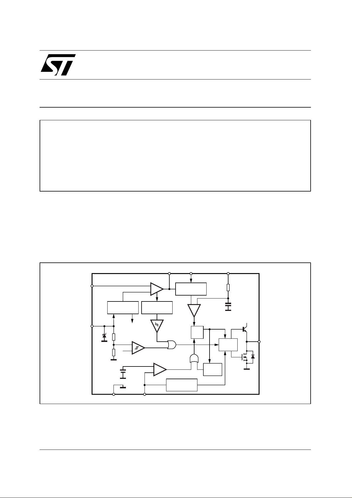
Figure 1 - L6561 Internal Block Diagram
COMP MULT CS
23 4
1
INV
V
-
2.5V
+
VOLTAGE
REGULATOR
8
CC
20V
R2
2.1V
1.6V
6
GND
INTERNAL
SUPPLY 7V
R1
V
REF2
OVER-VOLTAGE
+
-
5
ZCD
DETECTION
UVLO
ZERO CURRENT
+
-
DETECTOR
MULTIPLIER
+-
RSQ
DISABLE
5pF
STARTER
40K
DRIVER
D97IN547D
V
CC
7
GD
The outperforming L6561 offers a number of unique advantages that make the device an interesting alternative to the t raditionally used PWM controllers where quite a good performance is required at low
cost:
January 2003
1/11
AN1060 APPLICATION NOTE
disable function for power management and/or protection schemes;
•
true micropower start-up current, 50µA typ., for cost-effective start-up circuits;
•
very low quiescent current, 3mA typ., for high efficiency at light load;
•
two-level (static and dynamic) overvoltage protection (OVP);
•
on-chip RC filter on current sense pin for improved noise immunity;
•
pulse-by-pulse current limiting. In conjunction with TM operation, this ensures a safe operation under
•
short circuit conditions.
Refer to [1] for a detailed explanation of the internal architecture (shown in fig. 1) and the functionality of
the device.
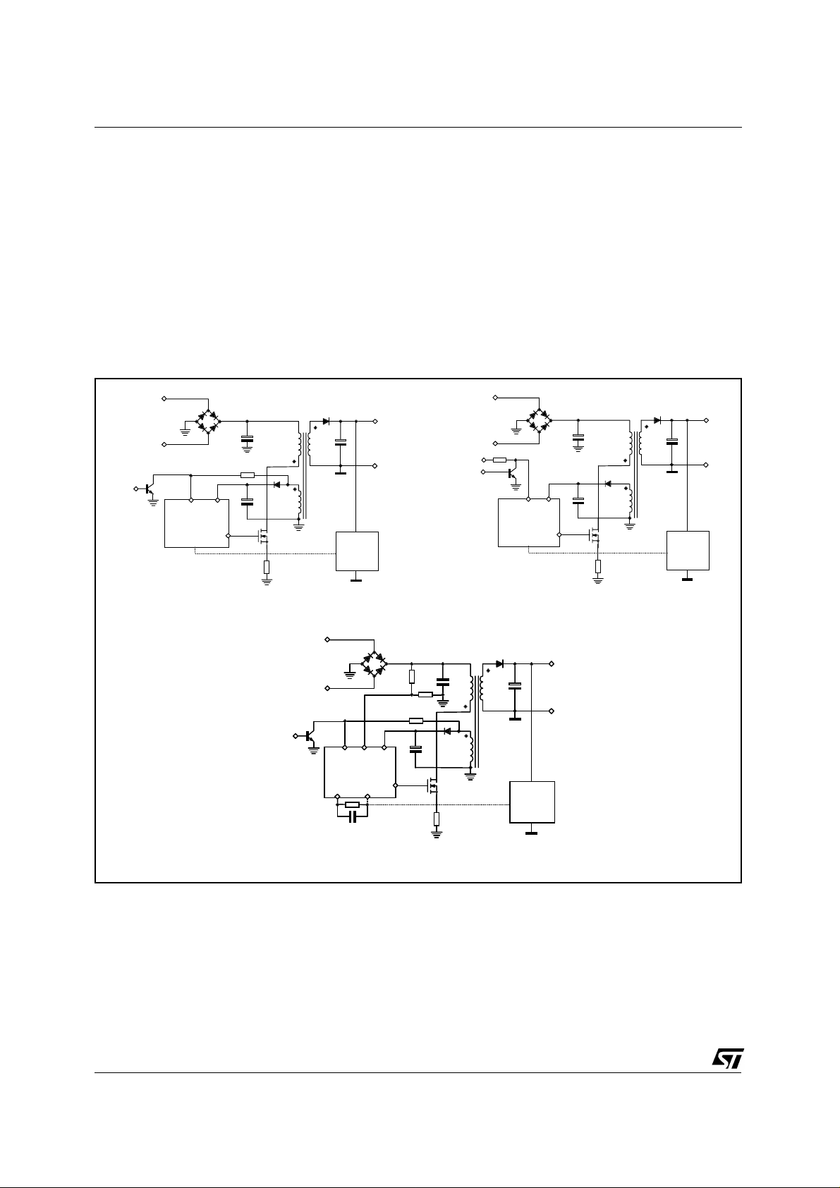
L6561-based flyback converters can be realised as schematically illustrated in fig. 2a, 2b, 2c, and which
will be referred to as "TM", "Synchronised" and "High-PF" respectively.
Figure 2. L6561-based flyback converter configurations
DISABLE
OPTO
TL431
Vout
+
Vac
VCCZCD
L6561
GD
BULK
C
a) TM Flyback
Vac
DISABLE
VCCZCD
MULT
IN
C
SYNCH
DISABLE
Vac
C
VCCZCD
L6561
GD
b) Sy nchronised Flyb ack
Vout
BULK
OPTO
TL431
Vout
+
L6561
GD
INV
COMP
OPTO
+
TL431
(BW<100 Hz)
c) High-PF Flyback
Each of them has its own peculiarities but they all share some key points:
low parts count, which helps reduce total cost and space;
•
high efficiency at very light load: an L6561-based flyback can be easily compliant with Blue Angel
•
standards;
standby function: the internal start-up timer may be used to make the system work at a (fixed) low
•
frequency under light load conditions, so as to minimise losses;
disable function: pin ZCD, if grounded, turns off the L6561 and reduces its consumption at a couple
•
of mA; this can be used either for power management or protection.
2/11
AN1060 APPLICATION NOTE
In the following, the three basic configurations will be taken into consideration and their advantages,
benefits and drawbacks will be highlighted so as to identify their most appr opriate field of application.
This will be made easier by some application examples.
TM Flyback
This configuration, very similar to a free-running flyback, always works on (actually, very close to) the
boundary between Continuous and Discontinuous Mode (i.e. Transition Mode, or TM), t heref ore at a frequency dependent on the input voltage and on the output current.
This type of operation requires a low induc tance and therefore a small-size magnetics but on t he other
hand, involves high peak current. Therefore it can be reasonably used for power levels up to 50-60 W in
110 V or wide-range mains applications, and up to 100 W with 220/240 V mains.
At high input voltage and especially at light load, the switch ON-time becomes very short and the switching frequency tends to become quite high. There is, however, a minimum ON-time (0.4-0.5µs) below
which it is not possible to go. This is due to the internal delay of the L6561 as well as the turn-off delay of
the MOSFET.
When this minimum is reached, TM operation can no longer be kept. The energy drawn each cycle exceeds the short-term demand from the load and the control loop delays MOSFET’s turn-on so as to
maintain the long-term energy balance. Switching becomes asynchronous, and this can be seen as a
"ghosting" of the waveform on the scope.
If the load is decreased furt her on, so many cycles need to be skipped that the amplitude of the drain
voltage ringing becomes very small, and the ZCD can no longer be triggered. In this case the internal
starter of the IC will start a new switching cycles sequence. Under this condition, the system will operate
in "burst" mode: there will be short periods of switching spaced out by long intervals where L6561’s OVP
keeps the switch in OFF state.
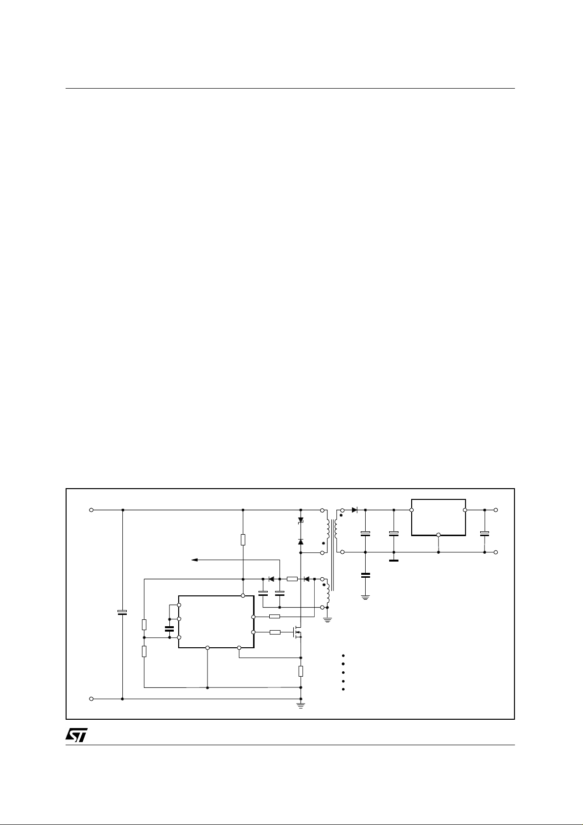
Fig. 3 shows a 7W power s upply, r ealis ed in TM flyback. It is intended as an auxiliary power supply suitable for systems provided with power management, such as monitor displays, printers, servers, photocopiers, fax machines, etc.
According to an approach that is becoming mor e and more popular, when the system is requested to go
into some low-consumption mode, a µP switches off the main SMPS. A small auxiliary supply, optimised
for a low power level, keeps alive the µP itself and the circuits needed for waking up the system again.
This approach allows to minimise the power consumption from the mains, in compliance with regulations
coming into force (such as Blue Angel and others).
Figure 3. 7W, Wide-range, Auxiliary Power Supply.
Vin=90 to 400 Vdc
BZW04- 154
Ω
Inpu t bulk capacitor
of the mai n S M PS
to L4990 A or L5991A
UC3843A/B or UC3 845A/B
or L4981A
100 nF
Ω
33 k
Ω
7.5 k
470 k
3
L6561
2
1
6
8
4
47 µF
5
7
1N4148
STD1NB60
STTA106
47 µF
47 k
Ω
22
22
Ω
Ω
1N4148
Ω
2
STPS360B
N1 N2
N3
TRANSFORMER SPECS:
CORE: E20x10x6, 3C85 material or equivalent
≈
0.5 mm air gap for a primary inductance of 1.7 mH
N1: 2 series windings 66 T each, AWG32
N2: 11 T, AWG24
N3: 21 T, AWG32
2x330
4.7 nF
µF
13
L4955V5.1
2
(∅0.57 mm)
5 Vdc / 1A
100
µF
(∅0.24 mm)
3/11
AN1060 APPLICATION NOTE
The converter is powered by the high-voltage DC bus, rangin g from 90 to 400 VDC, generated by the
front-end AC-DC stage (bridge rectifier + input capacitor) shared with the main SMPS (power factor corrected or not).
The output is post-regulated in order to provide a better regulation and supplies the µP as well as the
logic circuit needed to wake up the system.
The auxiliary winding will be properly designed so as to supply the controller(s) of the main SMPS besides powering the L6561. To minimise component count, a primary sensing feedback technique is
used.
The auxiliary winding is used also by the ZCD circuit for detecting transformer’s full demagnetisation and
turning on the MOSFET to start a new switching cycle (TM operation). The resistor driving the ZCD pin
is in the ten kΩ but can be optimised so as to achieve a "quasi zero-voltage turn-on" as described in Ref.
[1]. The optimum value depends mainly on the inductance of transformer’s primary winding and on the
of the power MOSFET, thus it can be found empirically after bench tests.
C
oss
With the component values shown in fig. 3 the wake-up time of the converter, that is the time the system
takes to start operating after being powered, does not exceed 3 s at 90 V
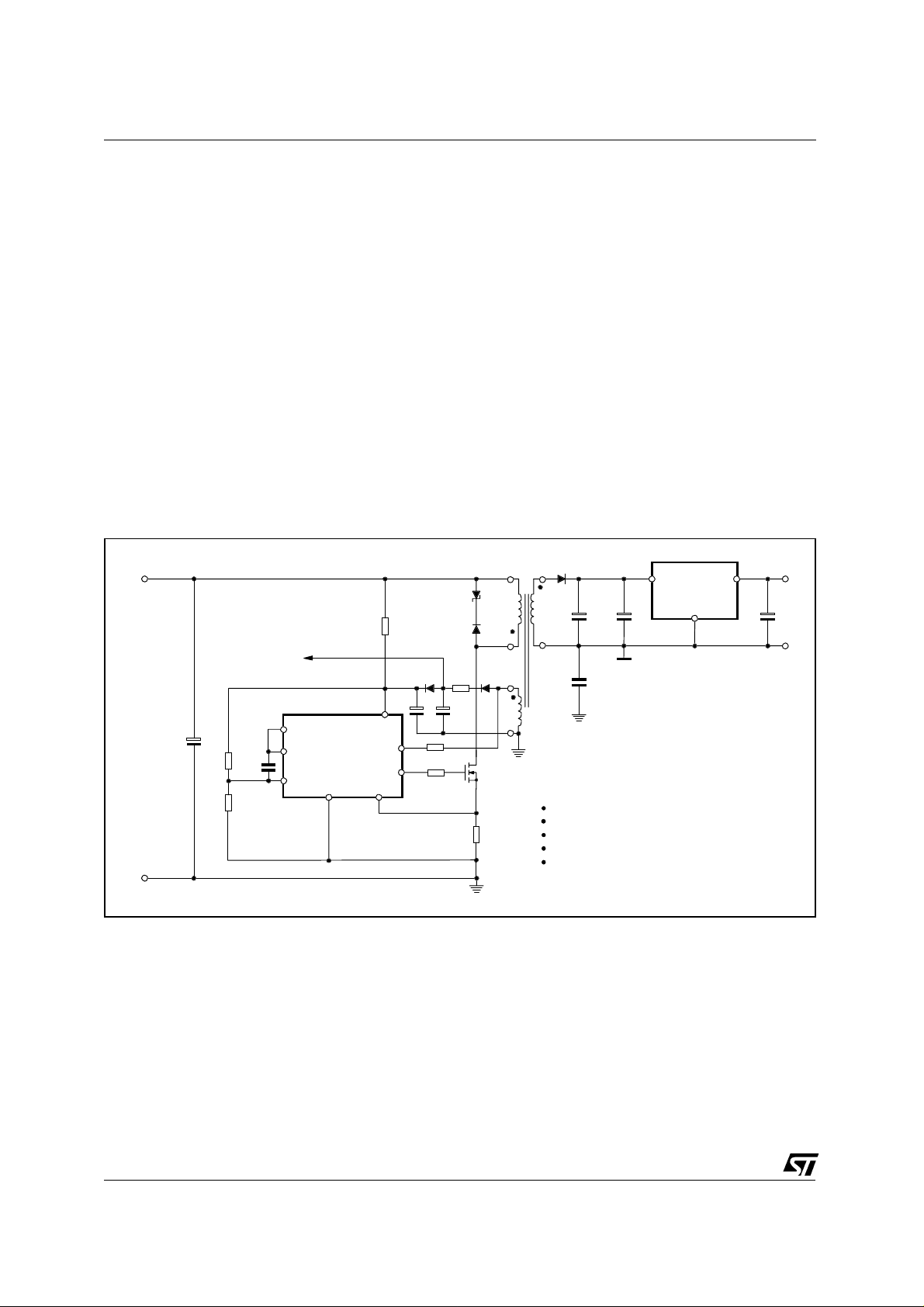
In fig. 4, the circuit of f ig. 3 is proposed with a different power rating: 15W output power so as to be able
to support USB function in computer equipment. The modifications concern the MOSFET, the transformer and the sense resistor on the primary side, the catch diode and the filter capacitors on the secondary side. They all have been increased in size.
Figure 4. 15W, Wide-range, Auxiliary Power Supply supporting USB function
supply and 1 s at 400 VDC.
DC
Vin=90 t o 400 Vd c
Input bulk capacitor
of the main SMPS
to L4990A or L5 991A
UC3843A/B or UC3845A/B
100 nF
Ω
33 k
Ω
7.5 k
or L4981A
BZW04-154
Ω
470 k
3
L6561
2
1
6
8
4
47 µF
5
7
STTA106
1N4148
22
STP3NB60FP
Ω
47 µF
47 k
Ω
22
1N4148
Ω
Ω
1
STPS560B
N1 N2
N3
TRANSFORMER SPECS:
CORE: E20x10x6, 3C85 material or equivalent
0.5 mm air gap for a primary inductance of 0.8 mH
≈
N1: 2 series windings 48 T each, AWG30
N2: 8 T, 2xAWG22
N3: 15 T, AWG32
2x1000
4.7 nF
µF
(∅0.24 mm)
13
L4955V5.1
2
(∅0.71 mm)
5 Vdc / 3A
220
µF
(∅0.30 mm)
Fig. 5 shows another example of low-power TM flyback application, an AC-DC adapter for battery
charger of cellular phones. The system looks very simple and very few parts are required.
The feedback uses a popular arrangement making use of a TL431 as secondary reference/error amplifier and of an optocoupler for transferring the control sign al to the primary side. This provides very good
regulation of the output voltage and galvanic isolation from the primary side at the same time.
The self-supply winding both powers the L6561and provides transformer’s demagnetisation signal to the
ZCD pin. The start-up cir cuit arrangement and its component values ensures that the wake-up time of
the converter does not exceed 3 s at 90 VAC supply (it will be less than 1 s at 270 V
AC
).
In fig. 6 an example of multi-output SMPS for inkjet printer is presented. The converter accepts input
voltages from 85 to 270 Vac and is rated for 40W output power. T he 28V output is used f or motors, the
12V output for the printhead and the 5V bus supplies the logic circuitry.
4/11

t
AN1060 APPLICATION NOTE
Figure 5. 7.5 W, Wide-range Mains AC-DC Adapter for cellular phones.
2200pF 2KV
2A fuse
N2
BYW98-100
2 x 470µF
85 to 270 Vac
4x1N40 07
10 µF
400V
110 k
BZW04-154
Ω
STTA106
Ω
47 k
N1
9V / 0.85A
16V
GND
4N35
3.3 nF
5
100 k
L6561
Ω
Ω
10 k
1N4148
F
µ
33
8
Ω
10
7
4
6
132
2
1/2 W
Ω
1 k
N3
STD1N B6 0
Ω
TRANSFORMER SPECS:
CORE: E19x8x5, 3C85 material or equivalent
≈
0.6 mm air gap for a primary inductance of
1.8mH
N1:170 T, AWG34 (∅0.20 mm)
N2: 15 T , 3x AWG34
N3: 19 T , AWG 34
4N35
TL431
Ω
1 k
0.022µF
1.8 k
Ω
4.7 k
Ω
The isolated feedback is realised with the configuration TL431 + optocoupler. Output cr oss-regulation is
improved by multiple sensing technique.
The system works in TM but can be forced to work at fixed frequency (that of L6561’s internal timer) for
minimum consumption at light load by the STANDBY signal (see fig. 6). This signal can be generated by
either the µP or a current sense circuit that enables low (fixed) frequency operation when t he load current falls below a defined threshold. To achieve this functionality, the ZCD pin is connected to ground
through a 4.3 kΩ resistor.
Figure 6. 40W, Wide-range Mains SMPS for Inkjet Printer.
STANDBY
DISABLE
47 k
47 k
85 to 270 Vac
Ω
Ω
2A fuse
5
3.3 nF
4.3 k
L6561
100 k
Ω
Ω
10 k
KBU4G
Ω
100
400V
132
4700pF 4KV
F
µ
110 k
8
7
4
6
1 k
Ω
Ω
56 k
Ω
2 W
STTA106
Ω
43 k
47µF
1N4148
STP4NA60FP
Ω
10
Ω
0.39
1/2 W
4N35
22 nF
250V
4.7M
N1
TL431
220
Ω
Ω
4700pF 4KV
4.7M
Ω
N2
N3
N4N5
4N35
2.7 k
BYW100-200
2 x 470µF
BYW98-100
2 x
1000µF
16V
BYW100-50
470µF
100 nF
Ω
TRANSFORMER SPECS:
CORE: ETD29x16x10, 3C85 material or equivalen
≈
N1: 6 9 T, AWG25
N2: 11 T, AWG25
N3: 9 T, AWG20
N4: 4 T, AWG25
N5: 1 1 T, AWG32
35V
16V
Ω
3.9 k
Ω
5.1 k
1 mm air gap for a primary inductance of 530 µH
(∅0.51 mm)
(∅0.89 mm)
(∅0.24 mm)
270 k
28V / 0.7A
12V / 1.5A
GND
5V / 0.5A
Ω
5/11

AN1060 APPLICATION NOTE
By directly grounding the Z CD pin, the converter will instead be shut down (DISABLE signal). This can
be used for either power m anagement ( an auxiliary supply like the one of fig. 3 will keep the µP alive) or
for protection, for example in case of overcurrent.
Pulse-by-pulse current limitation, inherent in the L6561, prevents input peak current from reaching too
high values. TM operation keeps pulse-by-pulse current limiting effective even under short circuit conditions and ensures that the transformer will never saturate.
Synchronis e d Fly back
L6561’s ZCD pin is intended for triggering MOSFET’s turn-on as the transformer is demagnetised, so as
to achieve TM operation. In this configuration the ZCD pin is used instead as a synchronisation input
and is driven by an external signal at a fixed frequency. This converter will then be exactly equal to a
synchronised flyback based on available standard current mode controllers.
A typical application of such a configuration is in multisynch monitors, where a synchronisation signal
coming from the horizontal deflection circuits of the display locks SMPS’ switching frequency so as to improve noise immunity.
An example of 17" multisynch monitor SMPS with the L6561 is shown in fig. 7. Capable of working with
wide-range mains, it is sized for 90W output power and can be synchronised from 31 to 82 kHz.
The primary side is extremely simple, yet the system features a number of functions needed in these
systems, such, overcurrent protection and synchronisation. There is also a protection against feedback
disconnection (the zener diode between the supply voltage and L6561’s pin 1).
Figure 7. 90W, Wide-range Mains SMPS for Multisynch Monitors.
85 to 270 Vac
SYNCH
(31 to 82 kH z)
DISABLE
47 k
47 k
5A fuse
Ω
Ω
KBU4G
220µF
400V
5
L6561
3
2
3.3 nF
1
Ω
100 k
Ω
10 k
TRANSFORM ER SPECS:
ETD44 core, 3C85 grade or equivalent
≈
1 mm air gap for a primary inductance of 38 0 µH
Ω
110 k
8
10
7
4
6
15 V
Ω
1 k
4N35
Ω
56 k
3W
STTA106
Ω
10
1N4148
47µF
Ω
Ω
Ω
1 k
1 k
1N4148
Ω
82 k
Ω
9.1 k
2.2 nF
N1 : 38 T, 2 series windings, 19T each, 4x AWG29 (∅0.29 mm)
N2 : 48 T, AWG25 (∅0.45 mm)
N3 : 32 T, AWG25
N4 : 3 T, AWG25
N5, N6 : 6 T, AWG25
N7 : 6 T, AWG32 (∅0.24 mm)
4700pF 4KV
4.7M
47 nF
250V
N1
N7
STP7NB60FP
0.47 Ω0.47
Ω
Ω
4700pF 4KV
Ω
4.7M
N2
N3
BYW100 - 100
N4
BYW100-100
N5
N6
BYW100-100
2.7 k
TL431
BYT11-800
STTA106
470µF 25V
470µF 25V
Ω
220µF
100V
4N35
330 pF
1000µF
16V
470 k
4.7 k
47
47µF 25V
1 nF
Ω
100µF
250V
Ω
Ω
100 k
200V
65W
80V
22µF
100V
Ω
330 k
10W
GND
6.3V
5W
+15V
5W
-15V
5W
Ω
6/11

AN1060 APPLICATION NOTE
In addition, a disable f unction is always available, which can be used f or any purpose the designer may
require.
Since the system works in Continuous Conduction Mode, especially at high switching frequency, a slope
compensation circuit has been added to prevent subharmonic oscillation at duty cycles greater than
50%.
Compared to the circuitry needed for a standard controller, the synchronisation interface is much simpler: just one resistor. Furthermore, when the synchronisation signal is missing, the system will run at the
frequency of the internal start-up timer (<15 kHz), which is lower than the minimum horizontal frequency.
Under this conditions the power demanded by the monitor circuits is usually very low, and the system
will go on working properly. This automatic functionality is extremely useful for minimising power consumption from the mains, again with the aim of meeting the relevant regulations.
High-PF Flyback.
This configuration works in Transition Mode t oo, but quite different ly from the TM flyback previously discussed. The input capacitance is here so small that t he input voltage is very close to a rectified sinewave. Besides, the control loop has a narrow bandwidth so as to be little sensitive to the twice mains frequency ripple appearing at the output. Ultimately, it is a PFC stage realised in f lyback topology, rather
than in boost topology as usual.
Actually, the high power factor (PF) exhibited by this topology can be considered just as an additional
benefit but not the main reason that makes this configuration attractive. In fact, despite a PF greater then
0.9 can be easily achieved, it is a real challenge to comply with EMC norms regarding THD of line current, especially in universal mains applications. There are, however, several applications in the lowpower range (to which EMC norms do not apply) that can benefit from the advantages offered by a highPF flyback converter.
For a given power rating, the input capacitance can be 200 times less, compared to a conventional flyback. The bulky and costly high voltage electrolytic capacitor located after the bridge rectifier is replaced
by a smaller low-cost film capacitor, with a considerable cut of cost and space.
Efficiency is high at heavy load, more than 90% is achievable: TM operation ensures low turn-on losses
in the MOSFET and the high PF reduces dissipation in the bridge rectifier. This, in turn, minimises the
requirements on the heatsink.
A few drawbacks, however, limit the applications that the high-PF flyback can fit (AC-DC adapters, battery chargers, low-power SMPS, etc.) and which one has to be aware of.
Because of the small input capacitance, the system is unable to cope with line missing cycles at heavy
load. Like in boost PFC stages, the transient response to step-load changes is poor: as to this point,
speeding up the control loop may lead to a compromise between an acceptable t ransient response and
a reasonably high PF.
The output voltage exhibits a considerable twice-mains-frequency ripple, unavoidable if a high PF is desired. Speeding up the control loop may lead to a compromise between a reasonably low output ripple
and a reasonably high PF. To keep the ripple low, a large output capacitance (in the thousand µF) is
anyway required: however, cheap standar d capacitors and not costly high-quality par ts are needed. In
fact, a low ESR and an adequate AC current capability are automatically achieved with so large a capacitance. Besides, in conventional flyback converters there is usually plenty of output capacitance too,
thus this is not so dramatic as it may seem.
As a result, secondary post-regulation will be required where tight specifications on the output ripple
and/or on the transient behaviour are given. This is true but is also what happens in numerous applications with a conventional flyback.
Please refer to Ref. [3] for a detailed explanation of the design of this kind of converter.
Fig. 8 shows the electrical schematic of a 30W AC-DC adapter based on high-PF flyback concept. It ac-
cepts universal mains and delivers 15V DC, 2A max. with a peak-to-peak twice mains frequency ripple
below 1V.
The multiplier is biased with a part ition of t he input voltage and provides a quasi-sinusoidal reference to
the current sense comparator. The feedback network uses a TL431+optocoupler configuration. Unlike
the previously considered ones, in this case opto’s transistor is connected as an emitter follower and
drives the input of L6561’s error amplifier. This aims at keeping the gain of the feedback and of the overall loop at twice mains frequency low, so as to achieve a high power factor.
7/11

AN1060 APPLICATION NOTE
Figure 8. 30W, Wide-range Mains, High-PF, AC-DC Adapter.
2A fuse
85 to 270
Vac
2.2 nF
DF06M
470 nF
20 k
4N35
P6KE170A
Ω
3 M
2
Ω
9.1 k
Ω
39 k
220 nF
Ω
20 k
2.4 k
3
L6561
1
6
Ω
Ω
470 k
Ω
STTA106
47 µF
8
5
10
Ω
7
4
STP4NA60
0.5
Ω
STPS8H100D 3x2200 µF
N1 N2
1N4148
N3
Ω
47 k
4.7 nF
DISABLE
TRANSFORMER SPECS:
Core: ETD29, 3C85 grade or equivalent
≈
1 mm airgap for 1 mH primary inductance.
N1: 2 series windings, 45 T each, AWG27 (∅0.41 mm)
N2: 14 T,5xAWG27
N3: 14T, AWG32 (∅0.24 mm).
5.1 k
4N35
1 µF
TL431
The optional 2.2µF capacitor connected in parallel to the upper resistor of the feedback divider acts as a
soft-start circuit. The diode between the capacitor and TL431’s control pin decouple the capacitor during
steady-state operation so that it does not interfere with t he loop gain. The other diode provides a discharge path when the converter is turned off, so that the system is always soft-started at power-up.
15 Vdc / 2A
Ω
Ω
12 k
2.2 µF
Ω
2.2 k
1N4148
Ω
2.4 k
1N4148
Figure 9. 30W, offline, High-PF battery charger with secondary post-regulation
2A fuse
85 to 270
Vac
220 nF 3 M
1 nF
DF06M
30 k
20 k
2xBZW0485
Ω
3
Ω
Ω
1 µF
5.1 k
2
1
Ω
220 k
5
L6561
6
Ω
47 k
47 µF
8
7
4
STTA10 6
Ω
Ω
22
Ω
10
STP5NA60
Ω
0.5
N1
1N4148
N3
STPS8H100D
N2
2200 µF
2200 µF
TRANSFORMER SPEC:
Core E25/13/7, 3C85 grade or equivalent
≈
0.7 mm air gap for a primary inductance of 720 µH
N1 : 2 series winding, 39 T each, AWG28 (∅ 0.37 mm)
N2 : 12T, 3xAWG26 (∅ 0.40mm)
N3 : 14T, AWG31 (∅ 0.23 mm)
Ω
20 k
1
2
22 k
4.7 nF
6
L4955
Ω
43
220
BAT46
7
5
Ω
2.7 k
1W
BAT46
Ω
15 Vdc / 2A
Ω
20 k
22 µF
Fig. 9 presents a 30W off-line, universal mains battery charger suitable for lead-acid batteries. Compared to the previous circuit, the primary side do es not change so much. The basic difference concerns
the feedback that here is based on sensing the voltage developed by the auxiliary winding.
This technique ensures a high PF in such flyback configuration because of t he poor coupling between
secondary and auxiliary winding at low frequency. It is then quite easy to get a gain low enough at twice
8/11

AN1060 APPLICATION NOTE
mains frequency. The drawback of primary sensing t ec hnique is its poor load regulation, but this is of no
concern in this case.
The post regulation on the secondary side with the L4955 linear regulator (see Ref. [4] for information)
ensures a high accuracy of the end-of-charge output voltage, as well as a precise constant current characteristic during battery charge. Additionally, the charge current can be adjusted from 1 to 2 A by means
of the 22 kΩ trimmer. The schottky diode in series to t he output prevents battery discharge when t his is
connected and the charger is off. The diode connected between pin 4 and pin 7 of the L4955 and the
220Ω resistor limit the current flowing in case of reverse battery connection.
Figure 10. 30W, High-PF battery charger with secondary voltage/current regulation
2A FUSE
85 to 270
Vac
20 k
1 nF
Ω
DF06M
470 nF
4N35
Ω
39 k
2.4 k
220 nF
Ω
9.1 k
20 k
Ω
2xBZW0485
100-200
10µF
50V
N1
BYW
N3
Ω
3 M
3
2
1
Ω
470 k
5
L6561
6
Ω
47 k
1N4148
47 µF
8
7
4
Ω
1
L78L12
2
10
Ω
STTA106
3
STP5NA60
Ω
0.5
STPS8H100D
560 µF
N2
2.2
15 Vdc / 2A
560 µF
4N35
Ω
10 k
Ω
k
100 nF
Ω
11 k
4.7 µF
0.1
2200
Ω
5.1 k
µF
Ω
2
8
1
5
100 nF
2200
2.2 µF
2.2 k
6
TSM
101
µF
Ω
12 k
Ω
130
1 µF
1.1 k
2.2 µF
1N4148
1N4148
Ω
Ω
3
7
4
TRANSFORMER SPE C:
Core E25/13 / 7, 3C 85 gra de or equi valent
≈
0.7 mm air gap for a primary inductance of 720 µH
N1 : 2 series winding, 39 T each, AWG28 (∅ 0.37 mm)
N2 : 12T, 3xAWG26 (∅ 0.40mm)
N3 : 25T, AWG31 (∅ 0.23 mm)
4.7 nF
The same battery charger can be realised without a post-regulator. Such a system is shown in fig. 10. It
uses again an isolated feedback with an optocoupler and a secondary side reference/error amplifier, the
TSM101, for voltage and current regulation.
This device basically incorporates a TL431 and two op-amps with or-ed outputs. One op-amp will be
used for constant voltage control and the other one for constant current control. A precise internal current generator, available at pin 3, can be used to offset the intervention threshold of the constant current
regulation. For more details, please refer to Ref. [5].
The voltage generated by the self-supply winding tracks the output voltage, which can be quite low (<9V)
when the battery is nearly exhausted. To let the system work even under this condition the self-supply
will deliver a voltage above L6561’s UVLO when the output voltage falls to its minimum. As a result,
however, when the charger is in voltage regulat ion (battery disconnected or end-of-charge) t he self-s upply voltage will exceed the maximum rating of the L6561. This requires the use of a linear regulator
(L78L12 in the present case) to limit the excursion of the voltage. The diode in series to the output of the
L78L12 prevents current diversion through the regulator at start-up.
The switch connected between TSM101’s pin 2 and ground enables/disables the above mentioned internal current reference. If t he switch is open, pin 2 is pulled up through the 10 kΩ resistor, the internal current generator is disabled and the constant current characteristic is set at 2A. If the switch is closed, pin
2 is grounded and t he internal current reference will be enabled. Pin 3 will be offset by about 160 mV
and the constant current threshold will be set at 0.3A.
9/11

AN1060 APPLICATION NOTE
Conclusions
The three basic configurations of L6561-based flyback converters have been presented. The common
characteristics, as well as the ones peculiar of each configuration have been analised.
A number of application examples has been presented for each category. They highlight how simple and
cheap but, this notwithstanding, well-performing L6561-based systems are.
It does not sound out of place, therefore, to say that the L6561 can be considered as a really inter esting
alternative to today’s high-runner current mode controllers, especially where quite good performance
and robustness are required at low cost.
References
[1] "L6561, Enhanced Transition Mode Power Factor Corrector", (AN966)
[2] "L6561-based Switcher Replaces Mag Amps in Silver Boxes", (AN1007)
[3] "Design Equations of High-Power Factor Flyback Converters Based on the L6561", (AN1059)
[4] "L4955 Family Application Guide", (AN932)
[5] "TSM101 Voltage and Current Controller", Datasheet
10/11

AN1060 APPLICATION NOTE
Information furnished is bel i eved to be accurat e and reliable. However, STMicroelec tronics assumes no responsibility for the consequences
of use of such inform ation nor for any infringement of patents or other rights of third parties which may result from its use. No license is
granted by implication or otherw ise under any patent or patent rights of STMic roelectronics . Specification mentioned in this publi cation are
subject to c hange without notice. Thi s publication supersedes and replac es all information previously su ppl ie d. S TMicroelectroni cs products
are not authorized for use as critical components in life support devices or systems without express written approval of STMicroelectronics.
The ST logo is a registered trademark of STMicroelectronics
© 2003 STMicroelectronics – Printed in Italy – All Rights Reserved
STMicroel ec tr on i c s GRO U P OF COMPANIES
Australia - Brazil - Canada - China - Finland - France - Germany - Hong Kong - India - Israel - Italy - Japan - Malaysia - Malta - Moro cco -
Singapore - Spain - Sweden - Switzerland - United Kingdom - United States.
http://www.st.com
11/11
 Loading...