

Page 1
AN1059
®
APPLICATION NOTE
DESIGN EQUATIONS OF HIGH-POWER-FACTOR
FLYBACK CONVERTERS BASED ON THE L6561
by Claudio Adragna
Despite specific for Power Factor Correction circuits using boos t topology, the L6561 can be s uccessfully used to control flyback converters. Among the various configurations that an L6561-based
flyback converter can assume, the high-PF one is particularly interesting because of both its peculiarity and the advantages it is able to offer. AC-DC adapters for mobile or office equipment, off-line battery chargers and low-power SMPS are the most noticeable examples of application that this configuration can fit.
This paper describes the equations governing such a kind of flyback converter with the aim of providing a number of relationships useful to the system designer.
INTRODUCTION
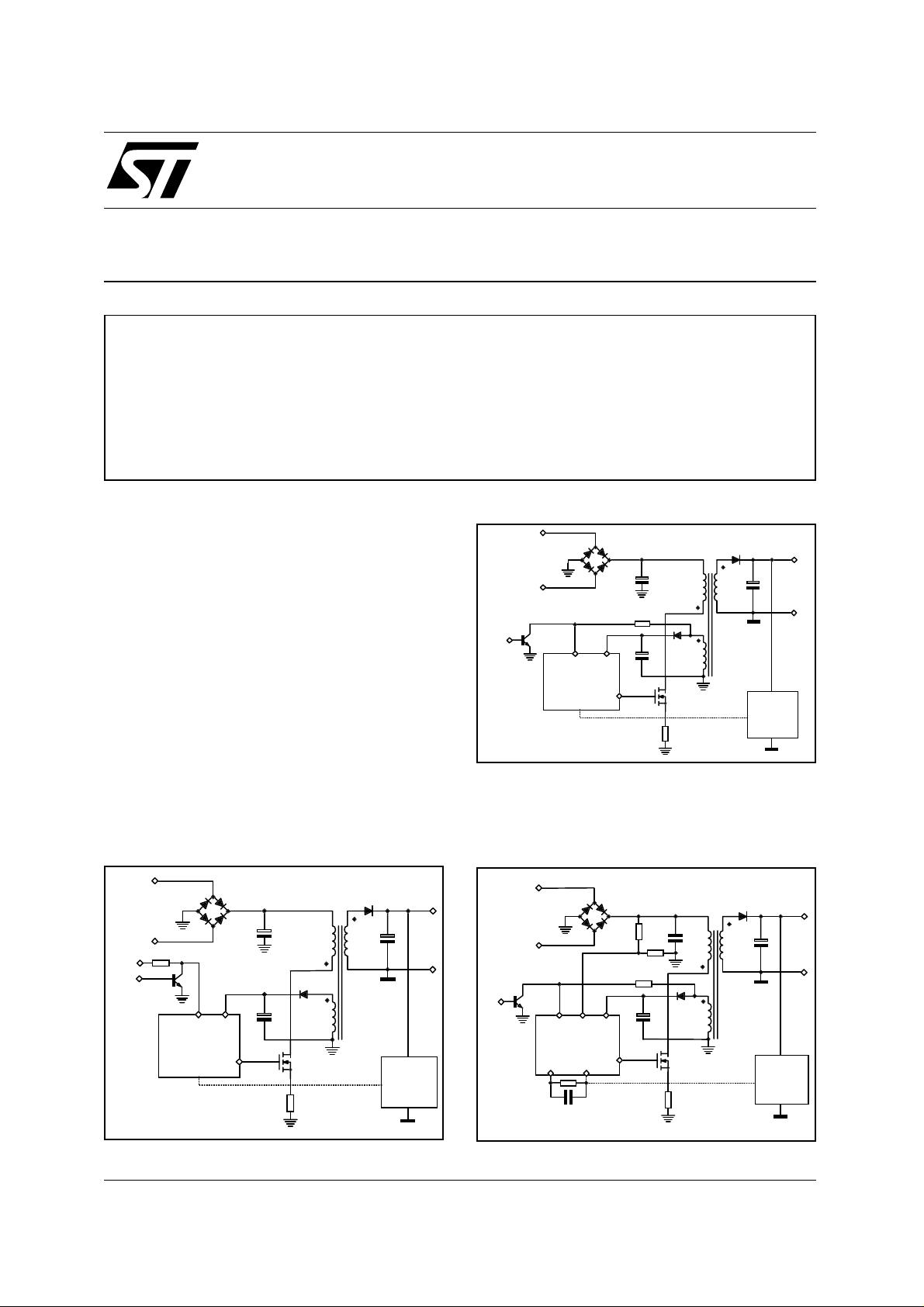
Three different configurations that an L6561-based
flyback converter can assume have been identified.
They are illustrated in fig. 1.
Configurations a) and b) are basically conventional
flyback converters. The former works in TM (Transition Mode, i.e. on the boundary between continuous
and discontinuous inductor current mode), therefore
at a frequency depending on both input v oltage and
output current. The latter works at a fixed frequency,
imposed by the synchronisation signal, and is ther efore completely equivalent to a flyback converter
based on a standard PWM controller.
Configuration c), which most exploits the aptitude of
the L6561 for performing power factor correction,
works in TM too but quit e differently: the input capacitance is so small that the input voltage is very close to a rectified sinusoid. Besides, the control loop
has a narrow bandwidth so as to be little sensitive to the twice mains frequency ripple appearing at the
output.
Figure 1a. TM Flyback Configurati on
Vac
DISABLE
VCCZCD
L6561
GD
C
BULK
OPTO
+
TL431
Vout
Figure 1b. Synchronis ed Fly ba ck C onfiguration
OPTO
+
TL431
Vout
Vac
SYNCH
DISABLE
L6561
September 2003
BULK
C
VCCZCD
GD
Figure 1c. High-PF Flyback Configuration
DISABLE
Vac
COMP
MULT
L6561
INV
VCCZCD
GD
C
IN
(B
W
Vout
OPTO
+
TL431
<100 Hz)
1/20
Page 2
AN1059 APPLICATION NOTE
Actually, the high power factor (PF) exhibited by this topology can be considered just as an additional
benefit but not the main reason that makes this solution attractive. In fact, despite a PF greater than 0.9
can be easily achieved, it is a real challenge to comply with EMC norms regarding the THD of line current, especially in universal mains applications.
There are, however, several applications in the low-power range (to which EMC norms do not apply) that
can benefit from the advantages offered by a high-PF flyback converter. These advantages can be summarised as follows:
for a given power rating, the input capacitance can be 200 times less, thus the bulky and costly high
●
voltage electrolytic capacitor after the rectifier bridge will be replaced by a small-size, cheaper film capacitor.
efficiency is high at heavy load, more than 90% is achievable: TM operation ensures low turn-on
●
losses in the MOSFET and the high PF reduces dissipation in the rectifier bridge. This, in turn, minimises requirements on heatsinks;
low parts count, which helps reduce encumbrance and assembly cost.
●
In addition, the unique features of the L6561 offer remarkable advantages in numerous applications:
efficiency is high even at very light load: the low current consumption of the L6561 minimises the
●
power dissipated by both the start-up resistor and the self-supply circuit. An L6561-based high-PF flyback converter can easily meet Blue Angel regulations;
additional functions available: the L6561 provides overvolt age protection as well as the possibility to
●
enable/disable the converter by means of its ZCD pin.
There are, on the other hand, some drawbacks, inherent in high-PF topologies, limiting the applications
that such a converter can fit (AC-DC adaptors, battery chargers, low-power SMPS, etc.) and which one
has to be aware of:
twice-mains-frequency ripple on the output: unavoidable if a high PF is desired. A large output ca-
●
pacitance will reduce its amount. Speeding up the control loop may lead to a compromise between a
reasonably low output ripple and a PF still reasonably high;
poor transient response: as to this point too, speeding up the control loop may lead to a compromise
●
between an acceptable transient response and a reasonably high PF;
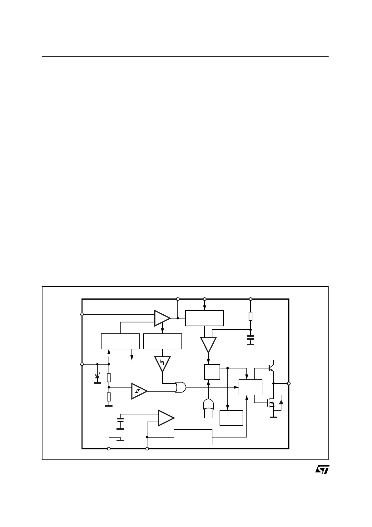
Figure 2. Internal Block Diagram of the L6561.
1
INV
V
VOLTAGE
REGULATOR
8
CC
20V
R2
6
2.1V
1.6V
GND
INTERNAL
SUPPLY 7V
R1
V
REF2
+
-
-
2.5V
+
OVER-VOLTAGE
DETECTION
UVLO
ZERO CURRENT
+
-
5
ZCD
DETECTOR
COMP MULT CS
23 4
MULTIPLIER
+-
RSQ
DISABLE
40K
5pF
DRIVER
STARTER
D97IN547D
V
CC
7
GD
2/20
Page 3

AN1059 APPLICATION NOTE
large output capacitance (in the thousand µF, depending on the output power) is required: however,
●
cheap standard capacitors and not costly high-quality parts are needed. In fact, a low ESR and an
adequate AC current capability are automatically achieved. Besides, in c onventional flyback converters there is usually plenty of output capacitance too, thus this is not so dramatic as it may seem at
first sight;
secondary post-regulation will be required where t ight specifications on the output ripple and/o r on
●
the transient behaviour are given. However, this is true also for a standard flyback;
the system is unable to cope with line missing cycles at heavy load unless an exceedingly high output
●
capacitance is used.
In the following, the operation of a high-PF flyback converter will be discussed in details and numerous
relationships, useful for its design, will be established.
Preliminary statements
In order to generate the equations governing the operation of a high-PF flyback converter working in TM,
refer also to the internal block diagram of the L6561(see fig. 2). For details concerning the operation of
the L6561, please refer to Ref. [1].
The following assumptions will be made:
1. the line voltage is perfectly sinusoidal and the rectifier bridge is ideal, thus the voltage downstream
the bridge, sensed by the input of the L6561’s multiplier (MULT, pin 3) is a rectified sinusoid:
V
(t) = VPK ⋅ |sin (2
in
⋅ π ⋅
fL ⋅ t)|
where V
is equal to the RMS line voltage, V
PK
, times the square root of 2, and fL is the line fre-
RMS
quency (usually 50 or 60 Hz).
2. the output of L6561’s Error Amplifier (V
) is constant for a given line half-cycle;
COMP
3. transformer’s efficiency is 1 and its windings are perfectly coupled.
4. ZCD circuit’s delay is negligible thus the converter works exactly on the boundary between continuous
and discontinuous current conduction mode (TM operation).
As a result of the first two assumptions, the peak primary current is enveloped by a rectified sinusoid:
I
pkp
(t) = I
⋅ |sin (2 ⋅ π ⋅ fL ⋅ t)| (1)
PKp
One consequence of assumption 3 is t hat the peak secondary current is proportional to the primary one,
depending on transformer’s primary-to-secondary turns ratio n:
I
To simplify the notation, in the following the phase angle θ = 2
(t) = n ⋅ I
pks
pkp
(t)
f
⋅ t of the sinusoidal quantities will
⋅ π ⋅
L
be indicated and all the quantities depending on the instantaneous line voltage will be considered as a
function of θ, instead of time.
Timing relationships
The ON-time of the power switch is expressed by:
L
⋅ I
p
T
=
ON
pkp
V
(θ)
in
(θ)
=
L
⋅ I
p
PKp
(2),
V
PK
where L
is the inductance of transformer’s primary winding. Eqn. (2) shows that TON is constant over a
p
line half-cycle, exactly like in boost topology. The OFF-time is instead variable:
L
p
T
OFF
=
⋅ n ⋅ I
L
⋅ I
(θ)
s
pks
V
+ V
(
out
2
n
=
V
(
)
f
out
pkp
+ V
(θ)
)
f
=
L
⋅ I
p
n ⋅ (V
PKp
⋅ |sin
+V
out
f
(θ)
)
|
(3),
3/20
Page 4

AN1059 APPLICATION NOTE
where Ls is the inductance of the secondary winding, I
voltage of the converter (supposed to be a regulated DC value) and V
(θ) the peak secondary current, V
pks
the forward drop on the output
f
the output
out
catch diode.
Since the system works in TM, the sum of the ON and the OFF times equals the switching period:
⋅ I
where V
= n ⋅ (V
R
+ Vf ) is the so-called reflected voltage.
out
The switching frequency f
T = T
= T
sw
L
p
+ T
ON
-1
, therefore, varies with the instantaneous line voltage:
=
OFF
f
=
sw
Lp ⋅ I
PKp
V
PK
V
PK
⋅
PKp
1 +
V
1 +
V
PK
R
⋅ |sin
⋅
(θ)
|
(4)
1
V
PK
V
R
⋅ |sin
(θ)
|
and reaches its minimum value on the peak of the sinusoid (sin (θ)=1):
f
sw min
=
V
Lp ⋅ I
PK
PKp
⋅
1 +
1
V
PK
V
(5)
R
This value, calculated at the minimum line voltage, must be greater than the maximum one of the internal starter of the L6561 (≈14 kHz ), in order to ensure a correct TM operation. To accomplish with this
requirement, the primary inductance L
will be properly selected (not exceeding an upper limit). Actually,
p
to minimise the size of the transformer, the minimum frequency will usually be selected quite higher than
15 kHz, say 25-30 kHz or more, so the value of L
needs not have a tight tolerance.
p
The duty cycle, that is the r atio between the ON-time and t he switching period, will vary with the instantaneous line voltage as well (because of the variation of T
), as it is possible to find by dividing eqn.(2)
OFF
by (4):
T
ON
Equations (2) and (4) show that T
D =
and T, respectively, can be short at will if I
ON
=
T
1 +
zero, especially at high input voltage. In the real-world operation, it must be c onsidered that T
1
V
PK
⋅ |sin
V
R
(θ)
(5’)
|
(i.e. the load) tends to
PKp
ON
cannot
go below a minimum amount and so will do the switching period as well. This minimum (typically, 0.4-
0.5µs) is imposed by the internal delay of the L6561 and by the turn-off delay of the MOSFET.
When this minimum is reached, the energy drawn each cycle exceeds the short-term demand from the
load, thus the control loop causes some cycles to be skipped so as to maintain the long-term energy balance. When the load is so low that many cycles need to be skipped, the amplitude of the drain voltage
ringing becomes so small that it can no longer trigger the ZCD Block of the L6561. In that case the internal starter of the IC will start a new switching cycles sequence.
Something similar applies to t he duty cycle as well, which eqn. (5’) predicts to be unity when θ = 0, that
is at the zero-crossings of the mains voltage. In reality, a number of parasitic effects cause T
ON
and T
OFF
not to follow the ideal relationships (2) and (3). The effect of that on the overall operation is however
negligible because the energy processed near a zero-crossing is very little.
In the following, the ratio bet ween the line peak voltage V
and the reflected voltage VR will be indi-
PK
cated with Kv:
V
PK
K
=
v
V
R
Energetic relationships
Apart from the duty cycle, all the quantities expressed in the timing relationships depend on the throughput power, which is represented in the above equations by I
, the peak primary current oc curring at
PKp
4/20
Page 5
the peak of the sinusoid of the primary voltage.
The following relationships relate I
to the input power Pin and allow both to explicate the timing rela-
PKp
tionships and to calculate all the currents circulating in the circuit.
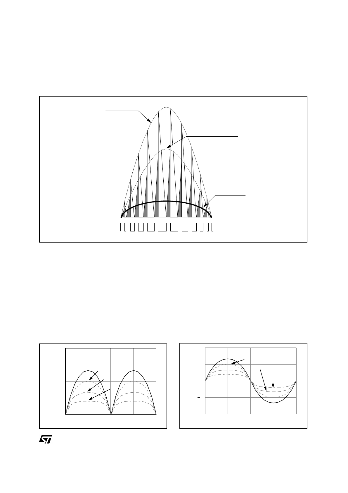
Figure 3. High-PF Flyback current waveforms
Secondary current
peak envelope
Primary current
peak envelope
AN1059 APPLICATION NOTE
Average
primary current
ON
OFF
The primary current I
SWITCH
(t) is triangular-shaped and flows only during the switch ON-time, as illustrated by
p
the shaded triangles shown in fig. 3. As earlier stated by equation (1), during each half-cycle the height
of these triangles varies with the instantaneous line voltage:
I
pkp
(θ) = I
⋅ |sin (θ)|,
PKp
their width is constant but they are spaced out by a variable amount given by (3).
Looking at the primary on a "f
" time scale, the current Iin(θ) downstream the bridge rectifier is the aver-
L
age value of each triangle over a switching cycle (the thick black curve of fig. 3):
|sin
|
0.5
1
0
0.5
(θ)
⋅ |sin
v
(θ)
Kv=0.5
|
Kv=1
Kv=2
Kv=4
1
(θ) =
⋅ I
(θ) ⋅
pkp
2
I
in
Figure 4a. Primary Current (@ fL time scale)
1
0.75
Iin(θ)
after the
bridge
Kv=0.5
0.5
0.25
Kv=1
Kv=2
Kv=4
D =
1
⋅ I
⋅
PKp
2
1 + K
Figure 4b. Line Current (@ fL time scale)
Iin(θ)
before
the
bridge
0
0 1.57 3.14 4.71 6.28
θ
1
0 1.57 3.14 4.71 6.28
θ
5/20
Page 6
AN1059 APPLICATION NOTE
This function, shown in fig. 4a for different values of Kv, is a periodic even function, at twice line frequency, not negative because of the bridge rectifier. Conversely, the current drawn from the mains will
be the "odd counterpart" of (6), at line frequency, as shown in fig. 4b).
Actually, it is realistic to think that a filtering action eliminates the switching frequency component of the
current upstream the rectifier bridge, so that the mains "can see" only the average value. This current
would be sinusoidal for K
Since K
cannot be zero (which would require the reflected voltage to tend to infinity), flyback topology
v
does not permit unity power factor even in the ideal case, unlike boost topology.
In order to simplify the following calculations, it is possible to eliminate the absolute value from | sin (θ)|
by considering θ ∈ [0 , π] and assuming the various functions to be either even or odd by definition, depending on their physical role.
The input power P
will be calculated by averaging the product Vin(θ) • Iin(θ) over a line half-cycle:
in
It is now advantageous to introduce the following function:
whose diagram as a function of the variable x is shown in fig. 5.
= 0 but will be distorted from an ideal sinusoid so much as Kv increases.
v
1 + K
sin2
sin
(θ)
2
⋅ sin
v
(θ)
(θ)
(θ)
dθ (8),
(7).
____________
P
= Vin
in
F2(x) =
Iin
(θ) ⋅
sin
1 + x ⋅ sin
(θ)
2
=
(θ)
1
⋅ VPK ⋅ I
2
=
(θ)
1
⋅ ∫
π
⋅
PKp
π
1 + x ⋅ sin
o
Figure 5. High-PF Flyback characteristic
functions : F 2(x ) dia g ra m
0.5
0.4
0.3
F2( )x
0.2
0.1
0
0123456789
x
Although a closed form exists for the integral in (8),
it is not so handy, thus for practical use it is more
convenient to provide a "best fit" approximation:
3
−
F2(x) ≈
0.5 + 1.4 ⋅ 10
1 + 0.815 ⋅ x
⋅ x
From (7), taking (8) into account, it is possible to
calculate I
10
PKp
:
2 ⋅ P
I
PKp
=
VPK ⋅ F2(K
in
,
)
v
which will assume its maximum value at minimum
.
mains voltage.
The total RMS value of the primary current, useful for power loss estimate on the primary side, is calculated considering the RMS value of each triangle of I
1
2
I
RMSp
√
=
⋅ I
pkp
3
(θ) ⋅
D = I
√
⋅
PKp
(t) and averaging over a line half-cycle:
p
1
3
⋅
sin
1 + K
2
⋅ sin
v
(θ)
(θ)
= I
PKp
√
⋅
F2 (K
3
)
v
(9).
The DC component of the primary current, useful to discriminate DC and AC losses in the transformer, is
the average value of I
(θ) over a line half-cycle:
in
_____
I
DCp
= I
=
(θ)
in
sin
1
⋅ I
⋅
PKp
2
1 + K
(θ)
⋅ sin
v
(10).
(θ)
Considering the following function:
F1(x) =
6/20
sin
(θ)
1 + x ⋅ sin
(θ)
=
1
π
⋅ ∫
π
sin
1 + x ⋅ sin
o
(θ)
(θ)
dθ,
Page 7

AN1059 APPLICATION NOTE
equation (10) can be rewritten as follows:
Figure 6. High-PF Flyback characteristic
I
DCp
=
1
⋅ I
2
functions : F 1(x ) dia g ra m
Also for F1(x) it is more practical to furnish a best fit
F1( )x
0.7
0.6
0.5
0.4
0.3
0.2
0.1
0
012345678910
I
o
(θ) =
x
1
⋅ I
(θ) ⋅ (1 − D) =
pks
2
approximation rather than the exact expression:
F1(x) ≈
0.637 + 4.6 ⋅ 10
As to the current on the secondary side, I
the series of triangles complementary to the primary’s (the white ones in fig. 3). Its twice line frequency representation will be again the average
over a switching cycle:
2
sin
⋅ sin
v
(θ)
(θ)
1
⋅ I
⋅ Kv ⋅
PKs
2
1 + K
Like the primary current (6), also (11) is a not negative periodic even function.
According to assumption 3), I
peak current is slightly less than n•I
possible to derive I
from the DC value of the output current, Iout, of t he c onverter, which is one of the
PKs
would equal n•I
PKs
because of transformer’s losses and other non-idealities) it is
PKp
. To consider a more realistic case (the secondary
PKp
design data.
By equalling the average value of (11) over one line half-cycle to I
2 ⋅ I
I
PKs
=
out
Kv ⋅ F2(K
.
)
v
, it is possible to find:
out
⋅ F1(K
PKp
1 + 0.729 ⋅ x
(11).
.
)
v
3
−
⋅ x
.
(t), it is
s
The total RMS secondary current is calculated as follows:
I
RMSs
______________
1
2
√
=
⋅ I
(θ) ⋅ (1 − D)
pks
3
= I
PKs
⋅
3
K
v
√
⋅
sin
1 + K
3
(θ)
⋅ sin
v
(12)
(θ)
It will be now introduced the third characteristic function of the high-PF flyback:
F3(x) =
3
sin
(θ)
1 + x ⋅ sin
(θ)
=
1
π
π
⋅ ∫
0
3
sin
(θ)
1 + x ⋅ sin
(θ)
0.424 + 5.7 ⋅ 10
dθ ≈
1 + 0.862 ⋅ x
With this definition, it is possible to express (12) as follows:
F3(K
)
I
RMSs
= I
PKs
⋅
√
K
v
⋅
v
.
3
Figure 7. High-PF Flyback characteristic
functions : F 3(x ) dia g ra m
For both primary and secondary side, t he AC component of current can be calculated with the general
relationship:
I
ACi
2
=
I
√
RMSi
− I
2
(i = p,s).
DCi
F3( )x
0.5
0.4
0.3
0.2
0.1
0
012345678910
4
−
⋅ x
.
x
7/20
Page 8

AN1059 APPLICATION NOTE
Power Factor and Total Harmonic Distortion
Under the assumption of a sinusoidal line voltage, the Power Factor PF can be expressed as:
V
PF =
where V
is the (effective) line voltage, I
RMS
phase with the line voltage) and I
can be simply calculated from the numerator of (13):
I
RMS1
It is worth noticing that I
RMSin
Real Input Power
Apparent Input Power
is the effective value of the f irst harmonic (it will be in
RMS1
the total effective value of the input current waveform (6).
RMSin
P
=
V
in
RMS
≠ I
I
RMS1
. In fact (9) contains also the energy contribution due to the switch-
RMSp
=
=
ing frequency, while equation (13) - and therefore I
I
is the RMS value of (6), which is by definition:
RMSin
I
RMSin
=
_____
2
√
I
in
(θ)
=
1
⋅ I
PKp
2
1
√
⋅
π
⋅ ∫
⋅ I
RMS
RMS1
V
⋅ I
RMS
RMSin
P
in
√2 ⋅
RMSin
(14).
V
PK
too - refers only to line frequency quantities.
π
sin
1 + K
0
v
Inserting (14) and ( 15) in (13) yields the theoretical expression of PF (note that it depends only on K
(θ)
⋅ sin
=
I
I
(θ)
RMS1
(13
RMSin
2
dθ (15).
)
v
Its diagram, depicted in fig. 8, shows how it keeps quite c lose to 1. For practical use, PF can be approximated by:
PF(K
) ≈ 1 - 8.1 ⋅ 10-3 ⋅ Kv + 3.4 ⋅ 10-4 ⋅ K
v
2
(16)
v
Obviously numerous non-idealities, basically the
ones mentioned in the section "Timing Relationships", contribute to achieve a real-world PF lower
than the theoretical value given by (16), especially
at light load and high mains voltage.
The Total Harmonic Distortion ( THD) of the line current is defined in percentage as:
∞
∑
2
I
RMS1
2
I
RMSn
,
√
THD % = 100 ⋅
Figure 8. Theoretical Power Factor of
high-PF Flyback converters
1
0.99
0.98
PF(Kv)
0.97
0.96
0.95
012345678910
Kv
).
where I
is the RMS amplitude of the n-th harmonic. Still under the assumption of an ideally sinusoi-
RMSn
dal input voltage, the THD is related to the Power Factor by the following relationship:
1
√
THD% = 100 ⋅
Fig. 9 illustrates the dependence of THD% on Kv.
For a given reflected voltage, it shows how the Total
Harmonic Distortion degrades when the line voltage
builds up.
Transformer
The design of the transformer is a complex procedure that involves several steps: selecting the core
material and geometry, determining the maximum
PF
− 1.
2
Figure 9. THD% as a function of Kv
40
32
THD%
(Kv)
24
16
8
0
012345678910
Kv
peak magnetic flux density (and whether this is lim-
8/20
Page 9

AN1059 APPLICATION NOTE
ited by core saturation or losses), determining the core size, defining the primary and secondary windings (turns number and wire gauge) as well as calculating the air-gap necessary to achieve the desired
inductance. Moreover, additional considerations concernin g the assembly are ne eded for meeting safet y
requirements, maximising magnetic coupling and minimising parasitic high frequency effects, not to
mention the constraints imposed by the specific application, if any.
Some parameters are needed to star t the design of the transformer. The (maximum) primary inductance
will be calculated by solving (5) for L
or by simply looking up the diagram of fig. 10, where the primary inductance required for 1W input power
is plotted against f
, for different values of K
swmin
value taken from fig. 10 (in mH), will be divided by the maximum input power to get the actual primary inductance required by the specific application.
The primary-to-secondary turns ratio will be given by:
Figure 10. Maximum specific primary inductance required
:
p
F2(K
1
L
≤
⋅
p
2
1 + K
)
vmin
vmin
and for the two typical mains voltage ranges. The
vmin
V
n =
V
out
.
⋅
R
+ V
f
swmin
V
f
2
PKmin
⋅ P
,
inmax
L( ),0.5 fmin
L( ),1 fmin
Lmax
L( ),1.5 fmin
[mH·W]
L( ),2 fmin
L( ),2.5 fmin
85
65
45
25
5
2 10
110Vac or
Wide-range Mains
6 10
L( ),0.5 fmin
L( ),1 fmin
L( ),1.5 fmin
L( ),2 fmin
L( ),2.5 fmin
4
vmin
K
= 0.5
1
1.5
2
2.5
4
3 10
4
4
4 10
fmin
fswm in [ H z ] fswmin [Hz]
5 10
4
Lmax
[mH·W]
400
300
200
100
0
2 10
220Vac Mains
vmin
K
= 0.5
1
1.5
2
2.5
4
3 10
4
4 10
fmin
4
5 10
4
6 10
4
With the peak and RMS current values calculated in the "Energetic relationships" section, the design can
be carried out just like for any conventi onal flyback transformer, thus no par ticular pr ocedure will be considered.
Anyway, as a design aid to core selection, two expressions for determining the minimum required core
Area-Product (winding window area times effective magnetic cross section) will be provided:
AP
min
=
f
swmin
AP
480 ⋅ P
⋅ (1 + K
=
min
in
) ⋅ √F2(
v
f
swmin
K
)
v
460 ⋅ P
⋅ (1 + K
1.585
) ⋅ √F2(
v
⋅ [ J
in
K
(
H
v
) ⋅
K
)
v
f
swmin
1.316
(17);
+ J
]
0.66
(18);
2
K
f
(
) ⋅
E
v
swmin
.
9/20
Page 10

AN1059 APPLICATION NOTE
where JH (Kv) and JE (Kv) are functions related to hysteresis and eddy current losses, whose best fit approximation are respectively:
1.87 + 1.26 ⋅ K
K
J
H
(
) ≈
v
1 + 0.55 ⋅ K
v
v
⋅ 10
5
−
J
E
K
(
) ≈
v
1.88 + 1.06 ⋅ K
1 + 0.34 ⋅ K
v
v
⋅ 10
10
−
.
Formula (17) assumes that the maximum peak flux d ensity inside the core is limited by core saturation
and that all transformer losses are located in the windings; (18) assumes that core losses limit the flux
swing and the total dissipation are half due to core losses and half to windings losses.
Figure 11. Minimum Transformer AP required for a
30W application.
1
0.9
Kv = 0.5
0.8
V( ),fmin 0.5
V( ),fmin 1
AP [cm ]
V( ),fmin 1.5
V( ),fmin 2
V( ),fmin 2.5
0.7
0.6
4
0.5
0.4
0.3
0.2
0.1
0
2 1042.5 1043 1043.5 1044 1044.5 1045 1045.5 1046 10
Kv = 1
Kv = 2.5
Kv = 1.5
Kv = 2
fmin
fswmin [H z]
Common to both formulae are the following
assumptions:
1. the material is a typical power ferrite
(3C85 from Philips, N67 from Siemens or
similar grades) with a saturation flux density
above 0.3 Tesla;
2. the windings occupy 40% of the total
window area to leave space for isolation layers, creepage and clearance distances;
3. primary and secondary winding wires
are proportioned for equal RMS current density;
4. core and/or copper losses result in 30 °C
hot spot temperature rise (no forced cooling);
5. skin and proximity ef fects are neglected,
considering the frequency range involved.
4
For a given f
lae (considering K
, one should try both for mu-
swmin
at minimum line voltage)
v
and use the higher resulting value. Core
losses become dominant for core selection above 45 kHz at this power level.
In fig. 11, the higher value resulting from (17) and (18) is plotted against f
considering 30W output power with an estimate of 85% efficiency.
for different values of Kv,
swmin
Figure 12a. RCD Clamp.
Clamp network
The overvoltage spikes due to the leakage inductance of the transformer are usually limited by an RCD clamp network, as illustrated in
fig. 12a. It can be advantageous the use of a zener (or transil) clamp
(see fig. 12b) when minimisation of power losses at light load is desired.
Considering the RCD clamp, the capacitor is selected so as to have an
assigned overvoltage ∆V (as a rule of thumb, half the reflected voltage)
at turn-off such that the voltage rating of the MOSFET is never exceeded. From energetic balance, it is possible to write:
2
L
⋅ I
lk
PKpmax
2 ⋅ V
,
)
R
where L
=
C
min
∆V ⋅ (∆V +
is the leakage inductance, which can be estimated in the
lk
range of 1 to 3% of the primary inductance if the transformer is properly
manufactured, and:
I
PKpmax
=
V
2 ⋅ P
PKmin
inmax
⋅ F2(K
vmin
)
The capacitor undergoes large current spikes and therefore it should
be a very low ESR type with polypropylene or polystyrene film dielectric.
10/20
R
C
D
Figure 12b. Zener (Transil)
Clamp.
T
D
Page 11

AN1059 APPLICATION NOTE
The minimum resistor value can be f ound by im pos ing that the voltage on the capacitor at the beginning
of each switching cycle never falls below the reflected voltage :
R
=
min
f
swmin
1
⋅ C ⋅ ln
1 +
V
∆
V
R
The power rating of this resistor can be estimated by c onsidering t he DC dissipation due to the reflected
voltage and the leakage inductance energy:
2
V
1
R
=
+
P
R
⋅ (1 + K
R
2
vmin
) ⋅
F2(K
vmin
) ⋅
L
lk
⋅ I
2
PKpmax
⋅ f
swmin
.
The blocking diode will be not only a very fast recovery type but will also feature a v ery fast turn-on time.
In fact, the instantaneous forward drop at turn-on generates a spike, exceeding the overvoltage ∆V, that
must be small. The diode will be rated for repetitive peak currents equal to I
voltage greater than V
PKmax
+ VR.
, and with a breakdown
PKp
Conside ring a zene r or a t ransil, its clampin g voltag e can be appro ximated wi th its bre akdown volt age. In
fact, the peak current is quite small and it is possible to neglect the contribution due to the dynamic resistance. The breakdown voltage, which should account for the drift due to the temperature rise, will then be:
≈ VCL = VR + ∆V.
V
(BR)
The steady-state power dissipation capability must be at least:
P
transil
=
2 ⋅ ( V
(BR)
(BR)
− VR
⋅ (1 + K
)
vmin
) ⋅
F2(K
vmin
) ⋅
L
lk
⋅ I
2
PKpmax
⋅ f
swmin,
V
while there is no concern about its peak power dissipation, since this is defined f or power pulses of 1 ms
(leakage inductance is typically demagnetized in less than 1 µs).
As to the blocking diode, what said earlier about the one of the RCD clamp still applies.
Output Capacitor
The output capacitor undergoes the AC component of the secondary current I
(t), (see fig 3).
s
Besides, to achieve a reasonably high PF, the voltage control loop is slow (typically, its bandwidth is below 100 Hz). As a result, there is a quite large voltage ripple appearing across the output capacitor. This
ripple has two components.
One is related to the high frequency triangles and depends almost entirely on the ESR of the output capacitor, being the capacitive contribution practically negligible. Its maximum amplitude, occurring on the
peak of the sinusoid, will be:
(HF)
= I
V
∆
o
PKs
⋅ ESR.
The second component of the r ipple is related to the t wice line frequency en velope and, unlike the high
frequency component, depends on the capacitance value, while the ESR contribution can be neglected.
To calculate the amplitude of t his component, only the fundamental harmonic of (11), at t wice line frequency, will be t aken into account. I n fact, the amplitude of t he higher order (even) harmonics is much
smaller and the impedance of the capacitor decreases with frequency as well.
According to Fourier’s analysis, the (peak) amplitude of the fundamental harmonic of (11) is:
v
⋅ ∫
π
sin
0
o2
π
⋅ K
I
PKs
I
=
(θ) ⋅
1 + K
cos(2 ⋅
⋅ sin
v
(θ)
θ)
dθ,
2
that, defining the following function:
11/20
Page 12

AN1059 APPLICATION NOTE
H2(x) =
1
π
sin
⋅
∫
0
cos(2 ⋅
(θ) ⋅
1 + x ⋅ sin
(θ)
θ)
dθ ≈
0.25 − 1.5 ⋅ 10
1 + 1.074 ⋅ x
2
π
3
−
⋅ x
(19),
can be expressed as:
H2(K
)
I
= I
o2
⋅ Kv ⋅ H2(K
PKs
v
) =
2 ⋅ I
out
⋅
F2(K
v
.
)
v
The absolute value in (19) is needed since the integral results negative, because the harmonic is 180°
out of phase. Finally, the peak-to-peak amplitude of the low frequency output ripple is:
V
= 2 ⋅ Io2 ⋅ Z
∆
o
H2(K
2fL
(
)
(C
1
⋅
) =
o
F2(K
π
I
)
v
out
⋅
)
v
fL ⋅ C
.
o
In most cases, once a capacitor is selected so as to meet the requirement on the low frequency ripple,
the ESR will be low enough to make the high frequency ripple negligible.
Multiplier Bias and Sense Resistor Selection
A resistor divider feeds a portion of the input voltage int o pin 3 (MULT) t o build the sinusoidal reference
for the peak primary current. To set properly the operating point of the multiplier the following procedure
is recommended.
First, the maximum peak value for V
MULT
, V
MULTpkmax
, is selected. This value, which will occur at maximum mains voltage, should be 2.5 to 3V in wide range mains applications and 1 to 1.5V in case of single
mains. The minimum peak value, occurring at minimum mains voltage will be:
V
V
MULTpkmin
= V
MULTpkmax
This value, multiplied by the minimum guaranteed ∆VCS/∆V
PKmin
⋅
V
PKmax
will give the maximum peak output volt-
COMP
age of the multiplier:
V
= 1.65 ⋅ V
If the resulting V
exceeds the linearity limit of the current sense (1.6 V), the calculation should be re-
cxpk
peated beginning with a lower V
multpkmax
cxpk
value.
MULTpkmin
In this way, the divider ratio will be:
V
MULTpkmax
K
=
P
V
PKmax
and the individual resistor values can be chosen by setting the current through them, in the hundreds µA
or less, to minimise power dissipation.
The value of the sense resistor, connected between the source of the MOSFET and ground, across
which the L6561 reads the primary current, is calculated as follows:
V
cxpk
≤
R
s
I
PKpmax
.
The resistor will be rated for a power dissipation equal to:
P
= Rs ⋅ I
s
2
PKpmax
⋅
F2(K
3
vmin
)
12/20
Page 13

AN1059 APPLICATION NOTE
Closing the C ontrol Loop
The control loop of a high-PF flyback converter based on the L6561, can be synthesised as in the block
diagram of fig. 13.
Unlike conventional converters, in such regulators the control loop will have quite a narrow bandwidth so
as to maintain V
sure a high PF. On the other hand, it is not possible to achieve a very high PF (>0.99), thus it makes no
sense to have a very narrow bandwidth (<20 Hz) like in b oost PFC preregulators. This would degrade
the transient response to line and load changes without any benefit. A compromise will then be found
between these two contrasting terms.
Figure 13. Block Diagram of the Control Loop of an L6561 - based high-PF flyback.
fairly constant over a given line cycle, as assumed at the beginning. This will en-
COMP
Vin
ZCD
Vref
+
Ve
ERROR AMPLIFIER
-
G1(s) G2(s) G4(s)
Vcomp
MULTIPLIER
FEEDBACK
H(s)
Vcx
+
PWM MODULATOR
IPKp
POWER STAGE
-
G3(s)
Vout
To the aim of deriving the transfer functions of the blocks in fig. 13, the narrow bandwidth of the control
loop allows to assume that the control action takes place on the peak amplitude of the various quantities.
The error amplifier (E/A) of the L6561 is compensated as illustrated in fig. 14. The transfer function
G1(s) will be then:
G1(s) =
∆
V
COMP
∆
R
=
−
V
E
R
7
⋅
1 + s ⋅ [C
6
1 + s ⋅ (C
⋅ (R7 + R
2
2
⋅ R
)
8
.
]
)
8
Figure 14. Compensation of the Error Amplifier.
R7
R8
COMP
_
E/A
+
TO MULT IPLIER
R6
C2
INV
2.5V
L6561
13/20
Page 14

AN1059 APPLICATION NOTE
The pole is placed at a very low frequency so that the gain at twice line frequency is quite less than
unity, while the zero boosts the phase in th e neighbour hood of the open-loop crossover frequency so as
to provide phase margin.
A variation ∆V
at the output of the multiplier. This considering, the transfer function of the multiplier block will be:
where KM is the gain of the multiplier (= 0.75 max.).
The gain of the PWM modulator, which includes the current loop, is simply:
where Rs is the sense resistor.
Small-Signal analysis shows that the gain G4(s) of the power stage is:
, due to a line and/or load change, modifies the amplitude Vcx of the rectified sinusoid
COMP
V
∆
G2 =
V
∆
COMP
G3 =
cx
= KM ⋅ KP ⋅ V
I
∆
PKp
=
V
∆
cx
PK
1
R
s
G4(s) =
V
∆
out
=
I
∆
PKp
n ⋅ K
Γ(
⋅ F2(K
v
K
+ 1
v
)
o
⋅
2
1 + s ⋅ (Co ⋅
1 + s ⋅ (C
)
R
v
⋅
⋅ ESR
o
K
Γ(
)
v
o
+ 1
)
,
)
R
where the function Γ(x) is defined as follows:
Γ(x) =
1 +
x
F2(x
⋅
)
dF2(x
dx
1 + 0.01 ⋅ x
)
≈
1 + 0.8 ⋅ x
.
The feedback network can have different configurations, depending on the requirements on the tolerance and on the regulation of the output voltage.
In this context a popular conf iguration (see fig. 15) will be taken into consideration. It uses an optocoupler for galvanic isolati on between primary and s econdary and a TL431, a cheap voltage r eference/opamp housed in a three pin package.
The gain, H(s), at twice line frequency must be low. In fact, being the output voltage ripple quite high, a
high gain could saturate the dynamics of the TL431 and/or of the optocoupler, besides complicating
things in getting a narrow overall bandwidth.
Referring to fig. 15, it is possible to write:
H(s) =
V
∆
E
=
V
∆
out
R
1
4
R
⋅
R5 + R
5
⋅ R
6
⋅ CTR ⋅
6
1 + s ⋅ C
s ⋅ (C
⋅ (R1 + R
1
⋅ R
1
1
)
3
,
)
where CTR is the Current Transfer Ratio of the optocoupler.
When designing the control loop, first select the operating current of optocoupler’s transistor (I
vantageous to selects a low I
value (e.g. 1 mA): this will not only extend the lifetime of the device but, in
C
). It is ad-
C
the present case, will also help keep low the gain of the feedback network at twice line frequency.
Since in closed-loop operation the quiescent value of V
reference of the L6561 E/A), R
will be:
5
will be in the neighbourhood of 2.5V (internal
E
2.5
R
=
.
5
I
C
R
will be selected so as to maintain VK voltage above 2.5V for a correct functionality of the TL431 even
4
in the worst case, that is when the optocoupler exhibits its minimum CTR, because of the statistical
spread of this parameter.
14/20
Page 15

AN1059 APPLICATION NOTE
Figure 15. Feedback network and connection to the error amplifier.
R6
R5
R
INV
<
4
COMP
L6561
VCC
C
I
V
− 1 − 2.5
out
2.5
V
TL431
K
F
I
R4
C1
⋅ CTR
min
R1
R3
R2
⋅ R5,
Therefore:
R7
R8
C2
V
E
Vout
≈
1 µF
where 1V is the typical drop across optocoupler’s photodiode. Keep R
close to the maximum for a low
4
gain. R1 and R2 are selected to get the desired output voltage:
V
2.5
R
=
; R1 =
2
I
R2
out
− 2.5
2.5
⋅ R
2
where 2.5 is the internal reference of the TL431 and IR2 the current flowing through R2.
To have a low gain at twice line frequency, the zero of H(s) wi ll be placed below 100Hz and R
5 times less than R
The value of R
. This yields the value of C1.
1
will be such that the twice mains frequency ripple superimposed on t he s tat ic VE cannot
6
will be 4-
3
trip the dynamic overvoltage protection of the L6561 (40 µA entering pin COMP). Approximately:
> R5 +
R
6
CTR
R
5
⋅
R
4
max
40 ⋅ 10
⋅ ∆V
6
−
o
R7 will be selected so as to allow t he output of the error amplifier to swing all the dynamics. Finally, R
and C2 will be adjusted so that the crossover frequency of the open-loop gain is a good compromise between a high enough PF and an acceptable transient response, ensuring also sufficient phase margin.
The optional capacitor (in the µF range) connected in parallel to R
acts as a s oft-start circuit that pre-
1
vents overvoltages of the output at start-up, especially at light load. The two diodes decouple the capacitor during steady-state operation s o that it does not int erfere with the loop gain and provide a discharge
path when the converter is turned off.
8
15/20
Page 16

AN1059 APPLICATION NOTE
CALCULATION EXAMPLE
An example of step-by-step design procedure of an L6561- based, high- PF flyback converter will be here
described for reference. It c oncerns a 30W AC adapter for por table equipment. The application was actually realised and some experimental results are here presented.
1. Design Specifications:
- Mains voltage range: V
- Minimum mains frequency: f
- DC Output Voltage: V
- Maximum output current: I
- Maximum 2f
output ripple: ∆Vo = 1V peak-to-peak
L
2. Pre-design Choices:
- Minimum switching frequency: f
- Reflected voltage: V
- Leakage inductance overvoltage: ∆V =70V
- Expected efficiency: η = 85%
3. Preliminary Calculations:
- Minimum Input Peak Voltage: V
(4V total drop on R
- Maximum Input Peak Voltage: V
- Maximum Output Power: P
- Maximum Input Power: P
- Peak-to-reflected Voltage Ratio: K
out
= 100V
R
DS(on)
= 88 Vac, V
ACmin
L
= 15 V
out
, Rs, ...)
out
=
in
= 50 Hz
= 2A
swmin
PKmin
PKmin
= V
out
P
out
⋅ 100 =
η
v
= 25 kHz
= V
= V
⋅ I
out
V
PKmin
=
= 264 Vac
ACmax
⋅
ACmin
√2 =
⋅
√2 =
ACmin
= 15 ⋅ 2 = 30W
30
⋅ 100 = 35.3W
85
120
=
V
R
100
= 1.2
88 ⋅
264 ⋅
√2 −4 =
√2 =
120V
373V
- Characteristic functions value: F1(1.2)=0.343; F2(1.2)=0.254; F3(1.2)=0.209; F5(1.2)=0.108
4. Operating Conditions:
- Peak Primary Current: I
- RMS Primary Current: I
- Peak Secondary current: I
- RMS Secondary Current: I
5. Transformer:
- Primary inductance: L
- Primary-to-secondary turns ratio: n =
From diagram of fig. 11, by interpolation, the minimum AP required is about 0.5 cm
ETD29 core (AP = 0.684 cm
16/20
=
p
PKp
RMSp
PKs
(1 +
2 ⋅ P
=
= I
=
RMSs
K
V
PKmin
PKp
= I
v
in
⋅ F2(K
F2(K
√
⋅
2 ⋅ I
out
Kv ⋅ F2(K
⋅
PKs
V
PKmin
f
) ⋅
swmin
3
)
v
√
Kv ⋅
⋅ I
V
V
+ V
(
out
4
), 3C85 grade is selected. From the relevant datasheet, wit h 1
=
120 ⋅ 0.254
)
v
)
v
= 2.32 ⋅
=
1.2 ⋅ 0.254
F3(K
3
=
PKp
R
=
)
f
2 ⋅ 35.3
√
2 ⋅ 2
)
v
= 13.1 ⋅
1.2) ⋅ 25 ⋅ 10
(1 +
100
15 + 0.6
= 2.32A
0.254
= 0.675A
3
= 13.1A
√
120
= 6.41
1.2 ⋅
3
0.209
3
⋅ 2.32
= 3.79A
= 940µH
4
. An
Page 17

mm air gap 90 primary turns will result in about 970µH primary inductance. 14 secondary
turns give a 6.43 turns ratio, very close to the target. Estimating the thermal resistance of the
ETD29 equal to 26°C/W, the maximum power dissipation (supposed to be on copper only) for
30°C hot-spot temperature rise will be 1.15W (half will be allocated to the primary and half to
the secondary). This requires the resistance of the primary to be no more than 1. 26 Ω and the
secondary’s no more than 40 mΩ. An AWG27 (
of 5xAWG27 for the secondary will meet the requirement.The primary winding will be split in
two halves of 45 turns each, series connected, and the secondary will be sandwiched in between to reduce leakage inductance.
6. MOSFET selection
- Maximum Drain Voltage:V
There is margin to s elect a 600 V dev ice. This will minimise gate drive and capacitive losses.
Assuming that the MOSFET will dissipate 5% of the input power, that losses are due to conduction only, and that R
about 2Ω. An STP4NA60 (R
0.4 mm) wire for the primary and a strand
∅ ≈
= V
DSmax
doubles at working temperature, the R
DS(on)
= 2.2 Ω max.) is selected.
DS(on)
+ VR + ∆V = 373 + 100 + 70 = 543V
PKmax
AN1059 APPLICATION NOTE
at 25°C should be
DS(on)
7. Catch diode selection
- Maximum reverse voltage: V
REVmax
=
A 100V Schottky diode will minimise conduction losses. As to it s current rating, a tentative
value can be 40% of the peak current: I
could be the STPS8H100D. From the relevant datasheet, the power dissipation is estimated
as: P
diode
= 0.48 ⋅ I
+ 0.013 ⋅ I
out
2
= 0.55 ⋅ 2 + 0.013 ⋅ 3.792 = 1.15W, which is acceptable.
RMSs
8. Output Capacitor Selection
The minimum capacitance value that meets the specification on the 100/120 Hz ripple is:
C
outmin
=
π ⋅
H2(K
1
⋅
F2(k
f
L
I
)
v
out
⋅
=
V
)
∆
v
o
0.108 ⋅ 2
3.14 ⋅ 50 ⋅ 0.254 ⋅ 1
Three 2200µF electrolytic capacitors will have an ESR low enough to consider the high frequency ripple negligible as well as sufficient AC current capability.
9. Clamp network
With a proper construction technique, the leakage inductance can be reduced to as much as
2% of the primary inductance, that is 20µH in the present case. A transil clamp is selected.
The clamp voltage will be V
= VR + ∆V = 100 + 70 = 170V. The steady-state power dissipa-
CL
tion is estimated to be about 2W. A P6KE170A transil is selected. The blocking diode is an
STTA106.
10. Multiplier bias and sense resistor selection
Assuming a peak value of 2.4V (@V
AC
value at minimum line voltage will be V
maximum slope of the multiplier, 1.65, giv es 1.32V peak v oltage on current sense (CS, pin 4).
Since the linearity limit (1.6V) is not exceeded, this is acceptable. The divider ratio will then be
2.4/(
264) = 6.43 ⋅ 10
√2 ⋅
-3
. Considering 120µA current for the divider, the lower resistor will
be 20kΩ, and the upper one 3MΩ.The sense resistor will not exceed 1.32/2.32 = 0.57Ω (0.5
is selected), while its power rating will be 0.5 ⋅ I
V
PKmax
n
+ V
= 0.4 ⋅ I
F
373
out
=
PKs
+ 15 = 73.2V
6.41
= 0.4 ⋅ 13.1 = 5.2A. A suitable device
= 5417µF
= 264V) on the multiplier input (MULT, pin 3), the peak
MULTpkmin
= 2.4 ⋅ 88/264 = 0.8V which, multiplied by the
2
= 0.5 ⋅ 0.6752 = 228mW
RMSp
Ω
11. Feedback and Control Loop
The selected optocoupler is a 4N35 from Toshiba. 1 mA quiescent collector current is selected. From opto’s datasheet, with 1mA collector current, the diode current can be between 1
and 2 mA approximately (0.5 < CTR < 1).
17/20
Page 18

AN1059 APPLICATION NOTE
An emitter resistor of 2.4kΩ, will give the desired collector current, thus the bias resistor
3
L6561
<
4
15 − 1.2 − 2.5
2.5
2.4
⋅
5.1
40 ⋅ 10
P6KE170A
Ω
470 k
STTA106
47 µF
8
5
Ω
10
7
4
STP4NA60
0.5
⋅ 0.5 ⋅ 2.4 = 5.4kΩ.
1 ⋅ 1
= 14kΩ. Select R6 = 20 kΩ. By selecting
6
−
STPS8H100D 3x2200 µF
N1 N2
1N4148
4.7 nF
N3
Ω
47 k
DISABLE
Ω
TRANSFORMER SPECS:
Core: ETD29, 3C85 grade or equivalent
≈
1 mm airgap for 1 mH primary inductance.
N1: 2 series windings, 45 T each, AWG27 (∅0.41 mm)
N2: 14 T,5x A WG27
N3: 14T , A WG32 (∅0.24 mm).
4N35
TL431
5.1 k
1 µF
Ω
12 k
2.2 k
2.4 k
15 Vdc / 2A
Ω
Ω
Ω
2.2 µF
1N4148
1N4148
should satisfy the inequality R
Select R
12kΩ. Select R
R
should be so that R6 > 2.4 ⋅ 103 +
6
R
= 39 kΩ, R7 = 9.1 kΩ and C2 = 220 nF, the open-loop crossover frequency and phase mar-
7
= 5.1kΩ. As to the output divider, with R2 = 2.4kΩ, the upper resistor will be R1 =
4
= 2.2 kΩ. With C1 = 1µF the zero will be at about 70 Hz, which is acceptable.
3
gin will be 50 Hz and 42° respectively.
The complete electrical schematic of this application is illustrated in fig.16, fig. 17 presents some results
of its bench evaluation and fig. 18 shows some significant waveforms.
Figure 16. 30W High-PF Flyback with the L6561: electrical schematic
2A fuse
88 to 264
Vac
2.2 nF
DF06M
470 nF
20 k
4N35
Ω
3 M
2
Ω
9.1 k
Ω
39 k
220 nF
Ω
20 k
2.4 k
1
6
Ω
Ω
Figure 17. 30W High-PF Flyback with the L6561: evaluation results
Efficiency [%]
100
90
80
70
60
50
18/20
Iout = 1A
Iout = 2A
120 180 240
Mains Voltage [Vac]
Iout = 0.5A
Iout = 0.1A
Power Factor
1
0.9
0.8
0.7
0.6
Iout = 2A
Iout = 1A
Iout = 0.5A
Iout = 0.1A
120 180 240
Mains Voltage [Vac]
Input Power [W]
1.4
Pout = 500 mW
1.3
1.2
1.1
1
0.9
120 180 240
Mains Voltage [Vac]
Page 19

AN1059 APPLICATION NOTE
Figure 18. 30W High-PF Flyback with the L6561: principal waveforms
= 90 VAC, P
V
in
Peak primary current envelope
Left :
Right, upper trace:
Right, lower trace:
= 30W
out
Mains current
Low-frequency primary current
References
[1] "L6561, Enhanced Transition Mode Power Factor Corrector", (AN966)
[2] "Flyback Converters with the L6561 PFC Controller", (AN1060)
19/20
Page 20

AN1059 APPLICATION NOTE
Information furnished is bel i eved to be accurat e and reliable. However, STMicroelec tronics assumes no responsibility for the consequences
of use of such inform ation nor for any infringement of patents or other rights of third parties which may result from its use. No license is
granted by impli cation or otherwi se under any patent or patent ri ghts of STMicro electronics. S pecifications mentioned in this public ation are
subject to c hange without notice. Thi s publication supersedes and replac es all information previously su ppl ie d. S TMicroelectroni cs products
are not authorized for use as critical components in life support devices or systems without express written approval of STMicroelectronics.
The ST logo is a registered trademark of STMicroelect roni cs.
All other names are the property of their respective owners
© 2003 STMicroelectronics - All rights reserved
STMicroelectronics GROUP OF COMPANIES
Australia – Belgium - Brazil - Canada - China – Czech Republic - Finland - France - Germany - Hong Kong - India - Israel - Italy - Japan -
Malaysia - Malta - Morocco - Singapore - Spain - Sweden - Switzerland - United Kingdom - United States
www.st.com
20/20
 Loading...