

AN1051
®
APPLICATION NOTE
TSM102 : A DUAL LI-ION BATTERY CHARGER
USING A N ST SILICON T RI PLE T
by A. BAILLY, D. CABROL, J. CAMIOLO
S. LAFFONT, R. LIOU
This application note explains how to use the VIPER20, the ST62 µController and the TSM102A in an
SMPS-ty pe battery charger which features :
.
Dual Li-Ion Battery charging with Constant Current/Cons tant Voltage
.
Battery type recognition (4.1V or 4.2V and different capacities )
.
Precision V oltage Control
.
Temperature and Failing Battery protection
.
End of Charge detection
1 - DEVICES PRESENTATION
The VIPER20 integrates on the sa me chip a PWM circuit together with a high voltage avalanche rugged
vertical MOSFET (600V, 0.5A) which make it ideal for primary side control of battery cha rgers or power
supplies featuring up to 20W output. Moreover, this device allows stand-by mode operation without
additional components.
The ST62T25C is a low cost 28 pins 8-bit Microcontroller available in Mask ROM, FastROM and OTP
versions. It features an A/D converter with up to 16 channels, 20 I/O pins of which 4 have High Current
capability . An integrated Static Reset circuitry , Oscillat or Safe Guard, 3 to 6 V power supply range and high
ESD tolerance make the device well suited for noisy envir onment.
The TSM102A integrated circuit i ncludes two Operational Amplifiers (type LM358), two Comparators (typ e
LM393) and one adjustable precision V oltage Reference (type TL1431 : 2.5V to 36V , 0.4% or 1%). TSM102A
can sustain up to 36V power supply voltage.
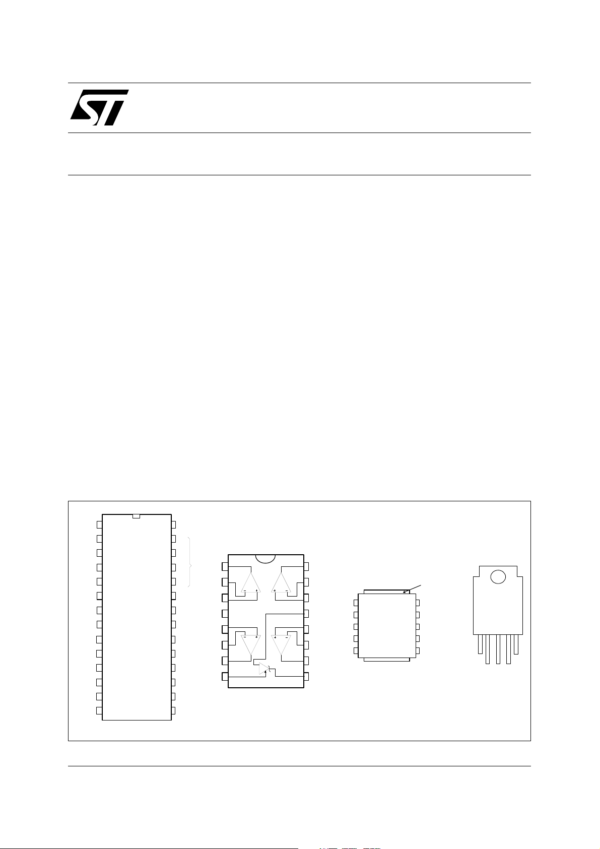
Figure 1 : ST62T25C, TSM1 02A and VIPER20 Pin
1
Vdd
2
TIMER
3
OSCin
NMI
PC7
PC6
PC5
PC4
TEST
PB7
PB6
PB5
4
5
6
7
8
9
10
11
12
13
14
OSCout
!RESET
February 1999
ST62T25C
DIP28 - SO28
Vss
28
PA0
27
PA1
26
20mA
V
CC
Vref
1
2
3
+
5
6
7
COMP
TSM102
COMP
PA2
25
24
PA3
23
PA4
22
PA5
PA6
21
PA7
20
PB0
19
18
PB1
17
PB2
PB3
16
PB4
15
16
15
14
V
-
CC
12
11
10
Cathode
OSC
COMP
Pentawatt-HV
PowerSO-10
6
Vdd
7
VIPER20
8
NC
NC
9
10
DRAIN
SOURCE
5
SOURCE
4
NC
3
SOURCE
2
SOURCE
1
VIPER20
1
234
OSC
5
COMP
Vdd
DRAIN
SOURCE
1/9
AN1051 - APPLICATION NOTE
2 - APPLICATION CONTEXT AND P RINCI PLE OF OP E RATION
The Li-Ion Battery
Rechargeable battery using Lithium have high voltage, big capacity and light weight, yielding an extraordinary energy density, more than twice the one of the NiCd. The maximum load current is not as high as
for the NiCd, but is still sufficient for many applications such as cellular phone and camcorder.
To improve lifetime and keep the battery in safe operating conditions, some protection circuitry is always
added inside the battery pack that can disconnect the electrochemical cell from the external connectors.
This protection circuitry is designed to trigger in case of overcurrent (both when charging and discharging),
overvoltage (when charging) and undervoltage (when discharging). The cell temperature is also mo nitored.
Charging Principle
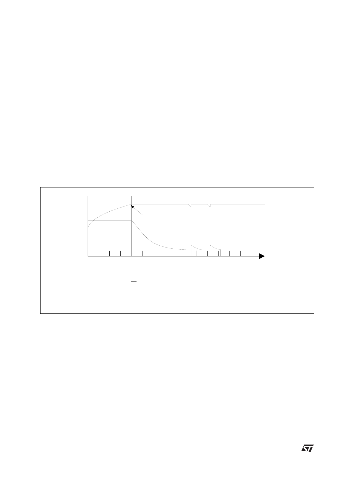
The charging principle of the Lithium-Ion batteries is very different from the Nickel type. Figure 2 shows the
different stages in the charging process. Time values are only indicative and depend on battery type and
speed of charge.
Figure 2 : Li-Ion Charging Scheme
Maximum cell voltage
I
V
Cell voltage rises
to voltabe limit
is reached
Occasional topping charge is
applied if battery voltage drops
15 30 45 60 75 90 105 120 135 150 165 180 minutes of charge
CONSTANT
CURRENT CHARGE
Maximum charge current
is applied until the set
voltage limit is reached.
1h
CONSTANT
VOLTAGE CHARGE
70% charged
Charge current starts
to drop as the battery
gets saturated.
2h
NO TRICKLE
CHARGING
100% charged
The Li-ion battery cannot
absorb over-charge. Trickle
charge would be harmfull.
During Stage 1, the battery is charged at consta nt current. The battery voltage is slowly increasing from
original voltage up to the maximum cell voltage, which depends on the battery electrode technology
(4.2V/cell for coke electrode, 4.1V /cell for gra phite electrode) .
Should this maximum voltage be exceeded and the battery could suffer significant damage and the
protection circuitry may tri gger.
Thus during Stage 2 a constant voltage charge is applied. Battery chargers manufactur ers recom mend a
highly precise voltage supervision of ±0.05 V/cell.
The current is slowly decreasing as the battery gets closer to full capacity .
End of charge can be detected by the charge current getting lower than a fixed threshold value (usually
one fifth to one tenth of the constant current charge value).
The dual Li-Ion Batteries charger :
In this application which requires ever increasing performances in more and more reduced space, the
silicon triplet VIPER20, ST62T25C and TSM102A provides an attractive soluti on in terms of performance,
cost efficiency and versatility.
2/9
AN1051 - APPLICATION NOTE
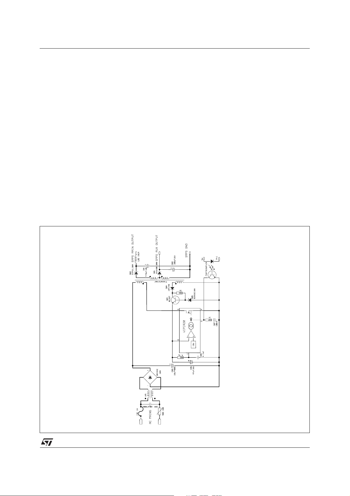
Figure 3a and 3b show the pri mary and the secondary sides of the battery charger (SMPS type, primary
and secondary sides) where the VIPER20, the ST62T25C and TSM102A are combined to ensure safe
charging of two Li-Ion battery cells in parallel (main and spare batteries).
The Viper20 ensures with a very low component count the energy transfer from the off-line primary side
to the secondary side thanks to its PWM ability ( with externally adjustable frequency of operation) and
integrated high voltage avalanche-rugged vertical MOSFE T.
The ST62T25C µController is used to :
• recognize the Li-Ion battery type (4.1V or 4.2V and capacity)
• manage the charging of the two different cells in parallel thanks to the proper command of two power
switches
• prevent the battery charging in case of overtemperature or undertemperature
• drive adequate LEDs for convenient visual information
The TSM102A can ensure all analog interfacing between the batteries and the µP by
• controlling current and voltage with adequate feedback via the optocoupler to the primary side
• offering highly precise voltage reference for all measurements
• amplifying the current signal through the sense resistor to be monitored by the µController
• providing a low cost solution for 5V power supply of the MCU
Figure 3a : Primary Side of Battery Charger
3/9

AN1051 - APPLICATION NOTE
In de tail :
a - The Primary Side :
The VIPER20 stands as a PWM circuit with integrated Power MOSFET after the Rectify ing-Filtering st age
(F01 fuse, R03 NTC, L02 and C04 filtering coil and capacitor, D03 diode bridge and C03 front bulk
capacitor).
R01 and D01 ensure the correct supplying of the VIPer20 device during normal operation thanks to the
auxiliary winding of the transformer . C05 is in charge of filtering this output, and provides also the needed
energy at start up thanks to the int egrated start up curr ent source of the VIP er20 device. The PWM funct ion
is determined by R02, D06 (frequency of operation) and the collector and emmitor of the photocoupler
(linear width modulation). The couple R04, C07 is a compensation network.
b - The Secondary side :
Figure 3b :Secondary Side of Battery Charger
4/9

AN1051 - APPLICATION NOTE
POWER SUPPLY :
Both ST62T25 C and TSM102A are supplied by a regulated 5V line. This line is regulated from the SMPS
Auxiliary output thank s to an NPN bipolar transis tor (Q1) polarized via its base by the integrat ed adjustable
precision V oltage referenc e of the TSM102A (R2, R3) . The base of Q1 is pulled up by R1 to ens ure proper
start up conditions and also to limit the current through the V oltage Ref erence during regulation mode. This
5V regulation circuitry is smoothen ed by the input and output capacitors C1 and C2.
VOL TAGE AND C URREN T RE GULATION :
The two comparators of TSM102A are used to regulate the v oltage and the charging curr ent of the batteries.
The first comparator compares the precise 2.5V Reference voltage with a part of the SMPS Main Output
(resistor bridge R4, R6) and the sec ond comparator c ompares the voltage drop t hrough the sense resis tor
R0 with a part of the regulated 5V line (resistor bridge R11, R12). The feedback to the primary side is
achieved thanks to the pair of ORing diodes (D1, D2) which pulls linearly the photocoupler (PH1) down via
the resistor R8. Compensation loops (R9, C3 and R10, C4) and output capacitors (Co1 and Co2) are added
to stabilize the voltage and current regulations.
BATTERY TYPE DETECTION AND CHARGE PARAMETERS ADJUSTMENT :
Pins C/F and V/F of the battery packs are used to provide charging voltage (V/F) and charging current
(C/F) information to the charger. Resist ors R30, R31, R35 and R36 are used to make resistor bridges with
internal battery pack resistors, which connect V/F and C/F pins to the battery pack ground pin as sho wn
on figure 4.
Figure 4 : Battery Pack Internal Schematics and P rinciple of Detection
+
V/F
C/F
-
+
to MCU A/D
MCU Gnd
Table 1 : BATTERY VOLTAGE DETECTION FROM V/F
V/F Resistor V/F Voltage 8 bit A/D Result Detected Battery Voltage
10k ±5% 2.375~2.625 117~138 4.1V
4.7k ±5% 3.29~3.51 163~183 4.2V
other other other no battery
T able 2 : BATTE R Y CURRE NT DETECTION FROM C/F
5V
+
C/F Resistor C/F Voltage 8 bit A/D Result Detected Battery Voltage
3.3 ~ 4.7k ±5% 2.375~2.625 119~136 400mA
2.4k ±5% 3.29~3.51 165~181 800mA
1.1k ±5% 4.02~4.17 203~205 1300mA
other other other no battery
5/9

AN1051 - APPLICATION NOTE
The µController is using A/D converters inputs P A6, P A7, PB2 and PB3 to measure respectively the voltages
on battery pack pins V/F1, C/F1, V/F2 and C/F2. Depending on these voltages the µController will switc h
various Open Drain pins to adjust the Voltage and Current regulation loops to the requirements of the
battery currently in charge.
Thus depending on the V/F pin voltage, the resistor R7 can be c onnect ed in parallel with R6 through PC4
which is configured in Open Drain mode. This will modif y the resistor bridge R4, R6, and will s et the voltage
regulation to 4.1V or 4.2V in respect with the battery type. The detect ion of the battery voltage is summarized
in Table 1. The 5% tolerance of the resistors, as well as the ±2 LSB accuracy of the Analog t o Digital
Converter are taken into account for the calculation.
In a similar way, and depending on the C/F pin voltage, the charge current is set to match the requirements
of the battery. PC5, PC6 and PC7, configured in Open Drain mode, command the PNP transistors Q2
(PC5), Q3 (PC6) and Q4 (PC7). When Q2, Q3 or Q4 (or the three at the same time) are on, the current
control value is modified according to the resistor bridge (R11, R12) modific ation (R14, R15, R16 in parallel
with R1 1). T he detection of the battery charge current is summ ariz ed in Table 2.
CURRENT FEEDBACK T O THE µ CO NTR OLLE R :
One Operational Amplifier of the TSM102A is used to zoom the current that flows through the sens e resistor
R0 (amplification loop R17, R19) so that this current information can be readable by the µController . The
µController acquires the data though PB7 configured as and A/D i nput.
2 SLOTS CHARGI NG FLOW :
In this specific application the first slot (A) is made to receive a complete handy phone while the second
one (B) is made to accommodate a spare batt ery. Thus the user c an charge both his phone + battery an d
a replacement battery.
To ensure efficient charging of both batteries cells (which are connected in parallel), the µController
commands two low Rdson P-channel MOSF ETs alternativ ely (Q5 and Q6 with PB4 a nd PB5).
If only one of the slot receives a battery (either A or B) the charger will perform a standard charge of that
battery by switching on the corresponding MOSF ET.
When the charger receives both the phone + battery (A) and the spare battery (B), the A slot has the priority .
Q5 will be turned on first and until A battery is full, B will be in Wait for Charge state, and Q6 will be off.
Only when A is full will B be c harged (Q5 off, Q6 on). As the phone in slot A may be on, and thus its battery
may discharge as B is on charge, the voltage of A slot is continuously monitored. If a significant drop is
detected, then the charger will enter an alternate charging mode where both batteries are charged on a
time sharing basis, so as to always keep the phone battery in full condition.
USER INTE RFACING :
The µController drives directly 2 bicolor LEDs (one for each battery) through PA0, PA1, PA2, PA3. The
meaning of the different signals in given in T able 3.
Table 3 : USER INTERFACE LEDs
State Green Red Bicolor Result Remark
No battery Off Off Off each slot
Charging Off On Red each slot
Full On Off Green each slot
Wait for charge On On Orange B slot only
Battery fail Blink Blink Orange Blink each slot
Over/Under temperature On On Orange only when charging
6/9

AN1051 - APPLICATION NOTE
PROTECTION/SAFETY FEAT UR E S :
The µController is checking the charging process in several ways so as to make sure that the battery is
kept into safe operating conditions.
.
Temperature is measured via resistor bridge R21 and R22 (where R22 is an NTC) and PB6 configured in A/D input. According to Li-Ion manufacturers information the cells should be charged only
when the temperature is between 0 and 45 °C. Thus when the temperature reaches outside this safe
operating range, the charging process is kept in standby (charge timings held, Power MOSFETs off
thus stopping the charge current, and user is warned of this condition by corresponding LED turning
orange). When the temperature is back to normal, charging process is resumed.
.
The 0 and 45 degrees threshold level have a programmable software hysteresis to prevent the
charger from oscillating form Temperature protection to Norm al mode.
.
Open battery condition is detected using current measurement throu gh PB7. If no current is flowing
for more than a programmable current establishment delay after the charge has started the battery
will be rejected, the charge terminated and the user warned of this condition by the corresponding
LED blinking orange.
.
Bad voltage battery condition : the µController is continuously monitoring the voltage of the batteries.
According to the battery manufacturers specifications, and depending on the voltage, the actions of
the charger are summarized in Table 4.
T able 4 : CHARGER STAT E AS A FUNCTIO N OF BATTERY VOLT A GE
Voltage State Action Condition
0 - 1.5V Pack protection circuitry active Trickle charge V > 1.5V within 1 second
1.5 - 2.7V Very low Trickle charge V > 2.7V within 30 minutes
2.7 - 4.1/4.2V Normal Standard charge V > 3.9V when battery is full
4.4V and over Overvoltage Stop charge -
The Condition Column shows what the result of the
action must be for the charger to proceed with the
charging. In case this condition is not fulfilled, the
battery will b e rejected, t he charge t erminat ed an d
the user warned of this condition by the corresponding LED blinking orange.
FULL BATTERY DETECTION :
This is made either by detecting a low current
flowing through the battery or by an overtime condition (maximum time after standard charge has
been started). A minimum voltage of 3.9 volt must
be reached at that time or the battery will be rejected, and the user warned of this condition by the
corresponding LED blinking orange.
3 - CALCULATION OF THE ELEMENTS
All the components values have been chosen for a
two-Lithium-Ion batteries charge application:
PWM Frequency and Maximum swithching ratio of the VIPER20 :
R02 > 1.2kΩ
Fsw = 2.3 Dmax / (R02 x C06)
Dmax = 1 - 550 / (R02 - 150)
recommended Dmax values are :
100kHz : Dmax > 80%
200kHz : Dmax > 70%
R02 = 4.7kΩ
C06 = 4.7nF
Dmax = 87.9%
Fsw = 9 1.5kHz
5V line power supply for TSM102A &
ST62T25C :
V out = V ref ( 1 + R2 / R3 )
R2 = R3 = 10kΩ
C1 = C2 = 10µF
R1 = 1.5kΩ
Voltage Control :
.
Vbatt = 4.100V
Vref = Vbatt x R6 / ( R6 + R4 )
With R6 = 100kΩ, R4 = 64kΩ
7/9

AN1051 - APPLICATION NOTE
If the battery is a 4.2V type, then, the resistor R7
will be connected in parallel to the resistor R6 by
means of the µController (PC4) :
.
Vbatt = 4.200V
Vref = Vbatt x (R6 // R7) / [ (R6 // R7) + R4 ]
Vref = Vbatt x [ R7 x R6 / ( R6 + R7) ] / [ R7 x R6
/ ( R6 + R7) + R4 ]
R7 = 1.6MΩ
Current Control :
.
Lowest current limitation : Ilim1 = 200mA, with
sense resistor R0 = 0.2Ω
Vlim1 = R0 x Ilim1 = 40mV
= Vcc x R12 / (R12 + R11)
with R11 = 10kΩ, R12 = 80.6Ω
.
Second current limitation : Ilim2 = 400mA
Vlim2 = R0 x Ilim2 = 80mV
= Vcc x R12 / (R12 + Rlim2)
OTHER COMP O NE N TS :
All other components values are indicated on the schematics
Notes :
.
When plugged in the sockets, the two batteries can have very different charge states (ie one is fully
charged and the other, almost empty). If no precaution is taken, and as long as the two batteries
voltages differ from more than 0.6V, a dramatic current flow can appear between the charged battery
towards the empty battery through the intrisic diodes of the power MOSFETS. This current is not
regulated and may either damage the MOSFETS, or trigger the over current protectio n system of the
battery pack itself and block the charging of the battery.
The schottky diodes D7, D8, the diode D6 and the PNP transistors Q7, Q8 solve this problem :
• no current can flow through the intrinsic diodes of the MOSFETS thanks to the schottk y diodes
• the voltage regulation is picked directly on the battery packs for increased precision thanks to the
PNP bipolar transistors used as low power analog switches
• the diode D6 prevents the voltage regulation from loosing its reference when the two Power
MOSFETS are OFF.
.
The current control values must be chosen in accordance with the elements of the prima ry side. The
global performances of the battery charger are highly dependent on the adequation of the primary
and the secondary elements.
.
R13 and R18 are the equivalent resistors seen from the opamp and from the comparator
(R13 = R11//R12, R18 = R17//R19)
.
C7 to C13 capacitors are optional filtering capacitors which ensure proper stabilization of the analog
values imposed to each of the corresponding A/D convert ers of the µController .
.
Transistors Q9 and Q10 are inserted to ensure good start up conditions (open collector until the µC is
correctly supplied).
.
An improvement to the integrated Voltage Reference’s line stability is shown on figure 5. The LED D’
(used as a visual "charger is ON" signal) polarized by the resistor R’ feeds the PNP bipolar transistor
Q’ with a quasi constant voltage which allows constant current to flow through the Vref. This regulated
5V line provides a very stable voltage even when the SMPS Aux Output varies from 7 to 30V.
Rlim2 = 4.957kΩ
Therefore, R14 = 9.83kΩ
.
Third current limitation : Ilim3 = 800mA
Vlim3 = R0 x Ilim3 = 160mV
Rlim3 = 2.438kΩ
Therefore, R15 = 3.22kΩ
.
Fourth current limitation : Ili m4 = 1.3 A
Vlim4 = R0 x Ilim4 = 260mV
Rlim4 = 1.469kΩ
Therefore, R16 = 1.72kΩ
where Rlim2 = R11 // R14
= Vcc x R12 / (R12 + Rlim3)
where Rlim3 = R1 1 // R15
= Vcc x R12 / (R12 + Rlim4)
where Rlim4 = R11 // R16
8/9

Figure 5 : Improved Voltage Reference Line Regulation
AN1051 - APPLICATION NOTE
Q1
R1
D'
Q'
R'
C1
Vref
C2
R2
R3
+5V
Caution :
Li-ion batteries have a very high energy density. Exercise precaution when handling and testing. Do not
short circuit, over charge, crush, m utilate, nail penetrat e, apply reverse polarity, expos e to high temperature
or disassemble. High case temperature res ulting from abuse of the cell could cause physical injury .
Information furnished is believed to be accurate and reliable. However, STMicroelectronics assumes no responsibility for the
consequences of use of such information nor for any infringement of patents or other rights of third parties which may result from
its use. No license is granted by implication or otherwise under any patent or patent r ights of STMicroelectronics. Specifications
mentioned in this publication are subject to change without notice. This publication supersedes and replaces all information
previously supplied. STMicroel ectronics products are not authorized for use as critical components in life support devices or systems
without express written approval of STMicroelectronics.
Australia - Brazil - Canada - China - France - Germany - Italy - Japan - Korea - Malaysia - Malta - Mexico - Morocco
The Netherlands - Singapore - Spain - Sweden - Switzerland - Taiwan - Thailand - United Kingdom - U.S.A.
© The ST logo is a trademark of STMicroelectronics
© 1999 STMicroelectroni cs – Printed in Italy – All Rights Reserved
STMicroelectronics GROUP OF COMPANIES
© http://www.st.com
9/9
 Loading...