

AN1049
®
APPLICATION NOTE
MINIMIZE POWER LOSSES OF LIGHTLY LOADED FLYBACK
CONVERTERS WITH THE L5991 PWM CONTROLLER
by Claudio Adragna
The L5991 PWM controller is particularly suitable for SMPS of equipment that must comply with
standards concerning energy saving. The device, optimized for fly back topology, monitors the power
demanded by the load and changes the operating frequency of the converter accordingly: high frequency at heavy load, low frequency at light load.
In this way, power losses dependent on frequency are reduced at light load maintaining, at the same
time, the advantages offered by a high switching frequency at heavy load.
The frequency reduction is very helpful but is not the only means needed to minimize power losses.
This note surveys the above mentioned f unctionality of t he L5991 (called "Standby" f unction) as well
as the most significant points to consider in order to achieve the goal of a very efficient lightly loaded
flyback.
INTRODUCTION
The minimization of the power drawn from the mains under light load conditions (Standby, Suspend or
some other idle mode) is an issue that is recently becoming of great interest, above all else because
new and more severe standards are coming into force.
This is already well-established in the area of computer monitors, where norms define precisely the various idle modes and the relevant maximum consumption admitted, but m ore and more often p ower supplies for other pieces of office equipment (i.e. printers, photocopiers, fax machines, AC-DC adaptors,
etc.), are required to accomplish with specifications concerning energy saving.
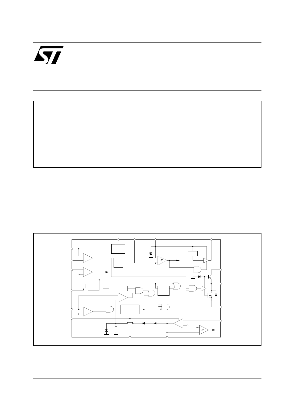
Figure 1. L5991 Internal Block Diagram
17V
VREF
48151
9
C
V
10
OUT
11
PGND
5
STANDBY
+
-
VFB
RCT
DC
DIS
ST-BY
ISEN
SS
2
3
14
16
13
1.2V
7
2.5V
+
-
+
STANDBY
OVER
CURRENT
+
-
DIS
VREF
BLANKING
1V R
SYNC
TIMING
T
PWM
DC-LIM
FAULT
SOFT-START
2R
12
SGND
21V
10V
V
VREF
OK
CLK
DIS
CC
+
-
SQ
R
6
COMP
PWM
UVLO
Vref
-
2.5V
E/A
+
2.5/4.0V
Anyway, minimizing the power wasted by a lightly loaded switch-mode converter is a demanding challenge for power supply designers and, to achieve the goal, an appropriate design strategy is required.
March 2000
1/24

AN1049 APPLICATION NOTE
The key point of this strategy is a low switching frequency. It is well-known that many of the power loss
sources in a lightly loaded flyback waste energy proportional ly to the switching frequency, hence this
should be reduced as much as possible. On the other hand, it is equally well-known that a low switching
frequency leads to bigger and heavier magnetics and makes filtering more troublesome.
It is then desirable to make the system operate at high frequency under nominal load condition and to
reduce the frequency when the system works in a low-consumption mode. This requires a special functionality of the controller: it should be able to recognize automatically the condition of light or heavy load
and should adequate its operating frequency accordingly.
The L5991 PWM controller, with its "Standby function", meets exactly this requirement. The function is
optimized for flyback topology: in fact, power supply of office equipment lies most often in the mediumlow power range, where flyback topology features the lowest cost/performance ratio and is, therefore,
the favorite one.
However, the goal of power losses minimization cannot be achieved with only a simple reduction of the
switching frequency. Although the most important, this is only one of the numer ous points of a wideranging strategy that must be looked into on the whole.
This application note is composed of two distinct parts. The first part deals with the L5991, describes the
operation of the "Standby function" in detail and states several relationships useful for the design. The
second one provides an overview of the points to be considered in the above mentioned strategy, as
well as a number of tips that can be helpful.
1) DESIGNING WITH THE L5991 PWM CONTROLLER
The L5991
The device, whose internal block diagram is shown in fig. 1, is based on a standard "peak" current
mode PWM controller, such as the UC384x family, with the addition of numerous ancillary features
among which Standby function is the most noticeable.
The L5991, which is available in DIP16 and SO16N packages, features the following characteristics:
;
;
7.0mA typ.
10.0mA max.
12mA typ.
17mA max.
yes
no
Very low start-up current (75 µA typ. - 120 µA max.)
low quiescent current (7 mA typ. - 10 mA max.)
internal reference with 1% precision guaranteed (@ Tj=25°C);
high current capability, large bandwidth, high slew-rate error amplifier;
high-speed current loop (< 100 ns delay to output);
high current capability totem-pole output for MOSFET or IGBT drive;
Standby function
;
IN/OUT synchronization;
precise maximum duty cycle control;
programmable soft-start
100 ns Leading Edge Blanking on current sense for increased noise immunity;
overcurrent protection with soft-start intervention;
latched disable function;
All these characteristics are described in detail in the datasheet of the dev ice. In this context, however, it
is worth emphasizing the low current consumption of the device, both before start-up and when running.
Along with the standby function, the low consumption turns out to be particularly useful for minimizing
losses.
Table 1 compares these characteristics with the UC384XA/B family.
Table 1. L5991 vs. UC384XA/B family
CONTROLLER START-UP CURRENT QUIESCENT CURRENT STANDBY FUNCTION
L5991 75µA typ.
UC384XA/B 300µA typ.
120µA max.
500µA max.
2/24
AN1049 APPLICATION NOTE
The L5991 can be used in off-line SMPS’ with any single-ended topology. However, i ts features make
the device particularly useful for power supplies based on flyback topology for office equipment that
must comply with standards concerning energy saving. Monitor displays, printers, photocopiers, scanners and fax machines are the most noticeable examples.
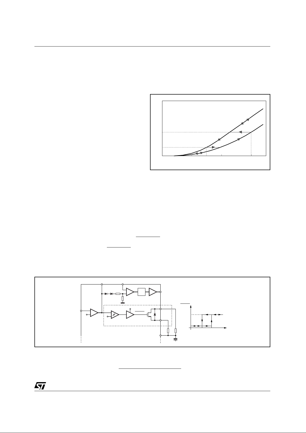
Standby function description
The L5991 automatically detects a light load
Figure 2.Standby function dynamic operation.
Pin
condition for the converter and decreases the
oscillator frequency on that occurrence. The normal (higher) oscillation frequency is automatically resumed when the output load builds up
and exceeds a defined t hreshold. This functionality is called "Standby function".
Like in every "peak" current mode controller, t he
output voltage (V
) of the Error Amplifier
COMP
(E/A) of the device moves depending on the
power drawn from the mains (see Appendix
"Peak Current Mode Control Basics"). The basic
principle of the Standby is then monitoring the
E/A output .
Normal operation
NO
P
SB
P
1234
V
1
T
Stand-by
V
VCOMP
osc
f
SB
f
2
T
If the peak primary current decreases as a result of a decrease of the power demanded by the load
will decrease as well. If this falls below a fixed threshold (VT1), the oscillator, which was working
V
COMP
, will be forced to work at a lower value (fSB). The frequency drop, however, implies a sudden in-
at f
osc
crease of the peak primary current and, therefore, of V
vent the frequency from s witching back to f
> VT1) in order for the oscillator frequency to be reset at f
(V
T2
. In fact, V
osc
. Some hysteresis will be necessary to pre-
COMP
will have to exceed a second threshold
COMP
. The hysteresis (VT2-VT1) will be large
osc
enough to prevent the above mentioned undesired phenomenon. This operation is shown in fig. 2.
Fig. 3 shows how the function is implemented internally. Only one pin (ST-BY, 16) is required and is
used to connect an external r esistor (R
) to the oscillator pin (RCT, 2). In this way, both the nor mal and
B
the standby frequency are externally programmable.
The capacitor C
mal operation (fosc). In fact, as long as the
the reference voltage VREF by a N-channel FET (see fig. 3), thus the timing capacitor C
and the resistor RB, along with RA, set the operating frequency of the oscillator in nor-
T
STANDBY signal is high, the pin is internally connected to
is charged
T
through RA and RB. When the STANDBY signal goes low the N-channel FET is turned off and t he pin
becomes floating. R
frequency (f
) will be lower.
SB
is now disconnected and CT is charged through RA only. In this way the oscillator
B
Figure 3. Standby function internal schematic and operation
COMP
6
5
FB VREF
+
2.5
66KΩ
+
-
2.5/4
STANDBY BLOCK
ISEN
13
2R
R
+
-
10V
LEVEL SHIFT
R
STANDBY
DRIVER
CUT
RCT
STANDBY
HIGH
LOW
RAR
B
C
T
D97IN752A
2.6V
V
V
T1
V
T2
COMP
4V
4
ST-BY
16
2
The oscillation frequency can be estimated with the following approximate relationships:
f
osc
≈
C
T
⋅ (0.693 ⋅ (R
1
⁄
⁄
A
RB
) +
(1),
K
)
T
3/24

AN1049 APPLICATION NOTE
which gives the normal operating frequency, and:
≈
f
SB
C
⋅ (0.693 ⋅ RA + K
T
1
(2)
)
T
which gives the s tandby operating frequency, that is the one t he converter will operate at when lightly
loaded. In the above expressions, R
and K
, defined as:
T
// RB mean s:
A
⁄
R
A
90, V
K
=
T
160, V
=
⁄
RB
RA + R
= VREF
15
= GND/OPEN
15
R
⋅ R
A
B
(3),
B
(4)
is related to the duration of the falling-edge of the sawtooth. I n case V15 is connected to VREF, however, the switching frequency will be a half the values resulting from (1) and (2).
Fig.3 shows also the comparator with hy ster esis t hat recognizes the load condition of the converter. The
thresholds V
and VT2 are internally fixed at 2.5 V and 4 V respectively (typical values). With reference
T1
to Fig. A1 in Appendix, the peak voltages on the current sense pin of the L5991 (ISEN, 13) relevant to
and VT2 are:
V
T1
− 2 ⋅ V
V
V
cspk1
cspk2
=
=
V
V
T2
T1
3
− 2 ⋅ V
3
2.5 − 2 ⋅ 0.7
f
=
4.0 − 2 ⋅ 0.7
f
=
= 0.367V (5)
3
3
= 0.867V (6).
It is more convenient to refer to the thresholds V
cspk1
and V
(rather than VT1 and VT2), because they
cspk2
can be immediately related to the peak input current. Although having fixed thresholds may seem a lack
of flexibility, in reality it is possible to adjust the thresholds in terms of input power level, if needed, by
adding a DC offset voltage (V
) on the current sense pin.
O
Standby Operation Analysis
In this context, flyback converters are c lassified as stated in the appendix "Flyback Basics". Another assumption is that the delay to output of the L5991 is compensated, thus the offset voltage Vo is intended
as the amount exceeding the value needed for compensation (see Appendix "Peak current mode control
Basics"). This analysis does not take other non- idealities into consideration, thus the results are approximate.
Please refer to the appendix for an explanation of symbols, terminology and formulas.
When V
= VT1, that is on the boundary of the standby mode, the peak input current is equal to:
COMP
− V
I
ppk1
=
V
cspk1
R
s
0.367 − V
o
=
o
(7),
R
s
corresponding to the standby inp ut power which, under the assumption of DCM (Discontinuous Conduction Mode) operation, can be expressed as:
0.367 − V
P
inSB
=
1
⋅ Lp ⋅ f
2
osc
⋅
R
The standby power can be expressed also in t erms of the maximum input power (P
the sense resistor R
vant to P
inmax
:
, which is selected so as to limit the peak primary current at the value (I
s
2
o
(8).
s
). This is set by
inmax
ppkmax
) rele-
4/24
1 − V
I
ppkmax
o
= (1 − V
o
R
=
s
√
) ⋅
2 ⋅ P
L
⋅ f
p
osc
(9).
inmax
AN1049 APPLICATION NOTE
By substituting (9) in (8) it is possible to obtain:
o
o
) ⋅
o
2
(10).
√
P
P
SB
inmax
⋅
f
√
osc
f
SB
(11).
inmax
⋅
1 − V
The frequency change f
P
= P
inSB
⇒ fSB pushes flyback into a deeper DCM operation and causes a sudden in-
osc
0.367 − V
crease of the peak primary current (since the input power does not change). As a result, the peak voltage on current sense will jump from V
V
’
cspk1
= Vo + Rs ⋅
√
cspk1
2 ⋅ P
LP ⋅ f
to:
SB
= Vo + (1 − V
SB
This value must be <V
the operating frequency to switch back and forth between f
not to exceed the hysteresis of the int ernal comparator, which would cause
cspk2
and fSB. This constraint sets a maximum
osc
limit on the frequency change:
f
f
osc
SB
0.867 − V
<
0.367 − V
Provided equation (12) is fulfilled, the input power (P
⇒ f
sumed (f
SB
) will be:
osc
P
inNW
1
=
⋅ Lp ⋅ fSB ⋅
2
2
o
(12).
o
) at which the normal operation frequency is re-
inNW
0.867 − V
R
2
o
(13)
s
which, considering position (9), can be also expressed in the following terms:
P
inNW
= P
inmax
⋅
1 − V
o
o
0.867 − V
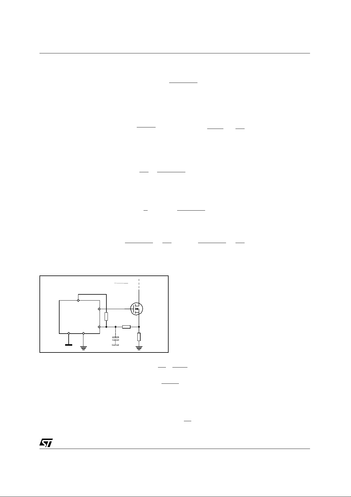
Figure 4. Circuit for the adjustment of the
standby thresholds.
R
= Vref
V
o
R + Rc
Vref
4
10
Rc
R
C
Rs
12
L5991
13
11
2
f
SB
⋅
f
osc
= P
inSB
0.867 − V
⋅
0.367 − V
The inspection of equations (8)...(14) shows that
adding an offset V
and P
inNW
/ P
(with respect to the values with Vo = 0).
This is equivalent to lowering the internal thresholds
and VT2. The effect will be more pronunciated
V
T1
than on VT2. In practice, the internal thresh-
on V
T1
olds have been fixed at the maximum value able to
allow high enough a frequency jump, with a certain
margin, leaving to an external circuit (like the one
shown in fig. 4) the duty of the adjustment, if necessary.
Referring now to MCM ( M ix ed Conduction Mode) and
2
o
⋅
o
lowers the ratios P
o
and raises the limit of f
inmax
CCM (Continuous Conduction Mode) systems, the
peak voltage on the current sense pin is given by:
f
SB
(14).
f
osc
inSB/Pinmax
/ f
osc
SB
where Z
=
V
cspk
is to be evaluated at fsw = f
E
+ Rs ⋅
V
o
Vo + Rs ⋅
osc
P
V
√
or fsw = fSB, depending on the operating mode. At the transition
in
+
E
2 ⋅ P
Z
E
V
E
P
2 ⋅ Z
E
in
Pin > P
CCM ↔ DCM the peak voltage on the current sense pin will be:
V
V
= Vo + Rs ⋅
cspkT
E
(16).
Z
E
in
> P
inT
(15)
inT
5/24

AN1049 APPLICATION NOTE
If the sense resistor Rs is selected as follows:
1 − V
o
I
ppkmax
o
). It will assume its minimum value at minimum mains volt-
osc
):
= Vo + (1 − V
(with Z
(with P
evaluated at fsw = f
E
and P
inT
age (that is, @ V
), the peak voltage on the current sense pin at transition will be given by:
osc
V
cspkT
evaluated at fsw = f
inTmin
= V
E
Emin
⇒ P
V
R
=
s
= Vo + (1 − V
= P
inT
inTmin
cspkTmin
Table A2 in appendix shows that in MCM systems (for which P
P
does not exceed 3.31 in practical cases. This means that also P
inTmin
As a result, the transition from CCM to DCM will occur at V
=
) ⋅
P
V
V
1 − V
inmax
Emin
V
E
Emin
o
) ⋅
⋅
+
V
2 ⋅ Z
P
inmax
1 +
o
(17).
Emin
E
2 ⋅ P
inT
+ P
2
P
inmax
P
inTmin
inTmin
values that do not exceed 2 / (1+3.31) =
cspk
(18),
inTmin
(19).
≤ P
inmax
inmax
≤ P
/P
) the ratio P
inTmax
will not exceed 3.31.
inTmin
inTmax
464 mV (when Vo = 0, and even larger values when Vo > 0).
In the end, since V
= 367 mV, when the L5991 activates the standby frequency MCM systems are
cspk1
operating in DCM. The s tandby input power will then be found once more from equation (8) which, accounting for (17) and after some manipulations, yields:
P
P
inSB
inmax
=
1
⋅
4
0.367 − V
1 − V
o
2
o
⋅
1 +
P
P
inmax
inTmin
2
P
inTmin
⋅
P
inmax
(20).
Besides, all the considerations leading to equation (12), as well as equation ( 12), still apply. This will always be true if V
cspkTmin
is greater than V
, that is if the ratio P
cspk1
inmax
/P
is such that:
inTmin
/
(= 4.45 for V
P
inmax
P
inTmin
= 0), which includes also a class of CCM systems. In practice, the above equations apply
o
1.633 − V
≤
0.367 − V
o
(21)
o
to the large majority of common flyback designs.
Once the system is in standby mode, in equations (15) Z
ZE’. This will modify also P
inT
, P
inTmin
and V
: they all increase and become P
cspkT
must be evaluated for fsw = fSB, becoming
E
respectively.
When V
, the system can be working either in DCM or CCM, depending on th e f
f
osc
is, on the input voltage). In other words, it depends on whether V
cspk
=V
, that is when the input power is P
cspk2
and the frequency is to be switched back to
inNW
is greater or less than V
cspkT’
possible to find that if the following condition:
1 +
P
P
inmax
inTmin
(22)
is fulfilled, then V
cspkT’
>V
cspk2
The right side of (22), for V
cal cases the f
/ fSB ratio will not be less than 2, it is possible to leave out the case of CCM operation.
osc
f
f
osc
SB
≥
0.867 − V
1
⋅
2
1 − V
V
o
Emin
⋅
o
⋅
V
E
and the system will be working in DCM.
= 0, is top limited at 1.87 in MCM systems. Considering that in most practi-
o
This makes things easier because there would be also a dependence of P
In the end, P
6/24
will be given again by equation (13) which, rearranged more conveniently, becomes:
inNW
P
P
inNW
inmax
=
1
⋅
4
0.867 − V
1 − V
o
2
o
⋅
1 +
P
P
inmax
inTmin
2
P
inTmin
⋅
P
inmax
⋅
f
, P
inT’
inTmin’
/ fSB ratio and on VE (that
osc
on VE.
inNW
f
SB
(23)
osc
and V
cspk2
cspkT’
. It is
f
f
f
f
AN1049 APPLICATION NOTE
The inspection of equations (15)...(23) shows that also in MCM systems the effect of the offset Vo is the
same as in DCM systems. Furthermore, the internal thresholds V
of applications can be covered without any external adjustment.
and VT2 are such that a large range
T1
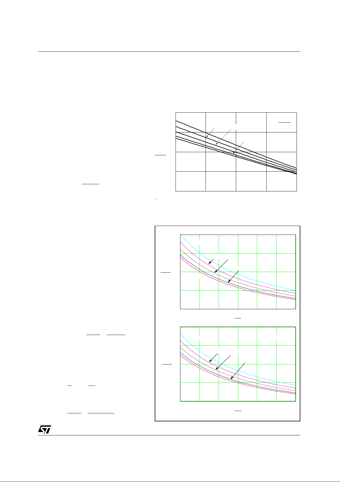
Standby func tion setup
It is difficult to out line a general procedure
for the use of the L5991’s standby function
because the constraints of a specific design
may be of different types and are not known
in advance. It is possible, however, to provide some diagrams that summarize the
analysis previously carried out and that can
be used for reference.
In figure 5 the ratio P
inSB/Pinmax
is plotted
against the offset voltage on current sense
, for different values of the parameter K
V
o
defined as:
P
K
In figure 6, the ratio P
against the ratio f
inmax
=
M
(24).
P
inTmin
inNW/Pinmax
/ fSB for the two ex-
osc
is plotted
treme values (0 and 200 mV) considered
.
for V
o
The inspection of such diagrams shows a
large influence of V
smaller influence on P
mainly on the ratio f
fosc and f
are both already fixed, there is
SB
on P
o
inNW
/ fSB. If the values of
osc
little room for the adjustment of P
, but a much
inSB
, which depends
. This
inNW
is not usually a problem because there is no
harmful effect if the converter is operating
= fSB even when the load is not so
at f
sw
light (e.g. 40% of the maximum load or
even more).
This considering, one possible step-by-step
procedure could be the following:
1. Check whether the flyback is DCM or
MCM. To this end, from table (A1) pick
up the value of V
specification value and calculate I
V
ppkTmin
=
I
relevant to the
Emin
Emin
Z
V
Emin
=
Lp ⋅ f
E
ppkTmin
osc
If the resulting value is great er than 1/Rs
then the system will be DCM, ot herwise
MCM.
2. Calculate P
use the following equation:
1
=
P
inmax
2
. If the system is DCM
inmax
2
1
⋅ Lp ⋅
⋅ f
(DCM)
osc
R
s
otherwise use:
P
inmax
=
V
Emin
R
s
−
2 ⋅ Lp ⋅ f
V
2
Emin
(MCM).
osc
Figure 5. P
in
P
P
in
M
Figure 6. P
:
inSB
/P
ratio vs. DC offset on current
inmax
sense.
20
M
= 3
K
M
= 2.5
/ P
K
inmax
ratio vs. f
15
M
≤1
K
10
SB
%
max
5
0
0 50 100 150 200
inNW
M
= 2
K
= 1.5
K
M
[mV]
o
V
/ fSB ratio for 0
osc
and 200 mV DC offset on current sense.
50
M
= 3
K
Q( ),,01z
Q( ),,0 1.5 z
NW
P
in
Q( ),,02z
max
in
P
Q( ),,0 2.5 z
Q( ),,03z
Q( ),,200 1 z
Q( ),,200 1.5 z
NW
in
P
Q( ),,200 2 z
max
P
in
Q( ),,200 2.5 z
Q( ),,200 3 z
40
30
%
%
K
20
10
2 2.5 3 3.5 4 4.5 5
50
M
K
40
30
M
≤ 1
K
20
10
2 2.5 3 3.5 4 4.5 5
M
≤ 1
= 3
M
K
= 2.5
M
K
= 2.5
M
= 2
K
M
= 1.5
K
z
osc
SB
M
= 2
K
M
= 1.5
K
z
osc
SB
M
K
o
V
max
in
P
=
P
inT
o
V
= 200 mV
min
= 0
7/24

AN1049 APPLICATION NOTE
3. Calculate P
inTmin
:
2
V
=
2 ⋅ Lp ⋅ f
Emin
osc
P
inTmin
4. Calculate K
5. In the diagrams of fig. 5, select the curve whose K
from (24).
M
value is closest to the one calculated in the pre-
M
vious step. Then find the offset voltage Vo to be applied to t he current sense pi n so that t he standby
power P
6. Select the curve whose K
depending on the value of V
the target value of P
7. Calculate the new value of R
is close to the target value.
inSB
value is closest to the one calculated in step 4 in either diagram of fig. 6,
M
selected in the previous step. The n find the f
o
, consistently with the constraints imposed by the specifications.
inNW
(R’s) needed to get the same P
s
’
R
= Rs ⋅ (1 − V
s
ratio that better fits
osc/fSB
:
inmax
)
o
Standby function and error amplifier compensation
The control loop of a L5991-based flyback must be stable over a very wide range of operating conditions. These include the entire input voltage range and an input power going from P
= f
operating at f
sw
and from P
osc
inmin
to P
at fsw = fSB. Moreover, the transition from standby mode to
inNW
inSB
to P
inmax
when
normal operation and vice versa must not have uncertainties. This requires the output of the error amplifier to react to frequency changes without overshoots and undershoots that exceed the other threshold,
thus causing the oscillator frequency to switch back and forth between f
SB
and f
And finally, when flyback operates in CCM, its control-to-output transfer function (dV
is the output voltage of the error amplifier of the L5991) feat ures the so-called RHP (Right-Half
V
COMP
osc
.
out
/ dV
COMP
, where
Plane) zero, which boosts the gain like a normal zero (a zero lying on the left-half plane) but lags the
phase like a pole. The RHP zero, which shifts with t he duty cycle, is diff icul t if not impossible to compensate and therefore must be kept well beyond the closed-loop bandwidth. This somet imes means that the
bandwidth must be narrow.
From what told above, to achieve stability under all operating condi tions, the error amplifier will need
quite a heavy compensation, such that the overall bandwidth may be even narrower than f
/4÷fSB/5,
SB
which one could expect. A s a result, the t ransient response of s uch a system will not be e xtremely fast.
On the other hand, the applications requiring the standby function do not have such a need.
2) OPTIMIZING TH E DESI GN FOR MAX IMUM EFFICIENCY AT LIGHT LOAD
Start-up & self-supply circuits.
Usually the start-up circuit is most commonly realized with a resistor (R
) that draws current from
START
the rectified and filtered DC bus (fig. 7 a). This solution is cheap but not the most efficient.
A reduction of the power dissipated at high mains voltage can be achieved by connecting the start-up re-
sistor to the AC side of the bridge rectifier through a low-voltage diode (see fig. 7b).
In both circuits, R
charge the supply capacitor (C
sured even at the minimum line voltage (V
R
START
.
In practice, however, R
dissipation especially at maximum mains voltage (V
is available to charge C
threshold (V
R
), the supply capacitor should be as low as possible, accounting for the time necessary for the
START
) of the IC, in particular at minimum mains. To reduce this wake-up time (having fixed
TH
carries the start-up current of the controller IC in addition to the one needed to
START
will be quite lower than t he maximum value, despite this increases power
START
and therefore the longer the supply voltage takes to reach the start-up
SUPPLY
) up to the start-up threshold of the IC. This current must be en-
SUPPLY
), which imposes a limit on the maximum value of
ACmin
). In fact, the higher R
ACmax
is, the less cur rent
START
self-supply circuit to take over and sustain the operation of the IC (see fig. 8).
8/24

Figure 7. Possible start-up circuit configurations
)
)
Vac
R
AN1049 APPLICATION NOTE
STAR T
Vac
1N4148
R
ST ART
L5991
12
a)
L5991
12
b
SUPPLY
C
C
SUPPLY
8
8
Vac
Ω
33 k
2 M
Ω
STD2N50-1
20 V
Csupply
47 k
4
Ω
8
L5991
12
c
9/24

AN1049 APPLICATION NOTE
Refer to appendix "Light load
Figure 8. L5991 supply voltage at start-up.
losses evaluation" for the calculation of the maximum R
START
and
an estimate of power dissipation
and wake-up time.
pin8
V
The circuit of fig. 7c is active only
during the start-up period, therefore it reduces dramatically the
power dissipated. Once the sys-
V
THON
V
CC
tem is running, the start-up MOS
is turned off and the only significant consumption is on the 2M
resistor (less than 20mW in a
wide-range mains application).
The components in the dashed
V
Ω
THOFF
voltage across C
SUPPLY
voltage generated by
the self-supply circuit
box can be omitted, provided the
supply voltage of the IC (V
18V or more, so that the gate-to-
CC
) is
WAKE-UP TIME
t
source voltage of the MOS is below the turn-on threshold.
This circuit can deliver several mA, thus the system will wake up very quickly. On the other hand, it requires several additional parts (mainly, a small high voltage MOS) and therefore has an impact on the
overall cost that needs to be evaluated by the designer.
The I
of the L5991 is low enough (120µA max.) to achieve a reasonably low consumption even
START
with circuits a) or b), whose main merit is to be inexpensive.
Table 2 compares the worst case consumption of the start-up circuits of fig. 7a) and 7b), at minimum
and maximum mains voltage. The table has been compiled assuming that the I C’s work in a system that
wakes up in 1s (@ V
) and where the self-supply circuit is able to keep the system operating within
ACmin
10 ms, at full load. The consumption of the gat e drive (see "Power MOSFET") is assumed to be 5mA
and ICs’ supply voltage is V
sumption would cause V
to fall below V
CC
=15 V. The UC3842A needs a bigger C
CC
before the above mentioned 10ms.
THOFF
because its higher con-
SUPPLY
Table2. Consumption of the start-up circuits of fig. 7 for 1s wake-up time (@ V
110V ±20% 220V ±20% Universal Mains
Device C
L5991 33µF a) 215 55 140 430 130 300 215 55 600
UC3842A 47µF a) 110 110 270 220 250 580 110 110 1170
SUPPLY
Start-up
circuit
R
START
(kΩ)
b) 55 55 130 130 105 250 55 55 590
b) 27 110 270 68 200 470 27 110 1190
(mW)
P
START
min. max. min. max. min. max.
R
(kΩ)
START
P
START
(mW)
R
START
(kΩ)
As to the self-supply circuit, usually it develops the voltage VCC (obviously greater than V
ACmin
).
P
START
THOFF
(mW)
) by rectifying and filtering the voltage generated by an auxiliary winding of the flyback transformer (see fig. 7).
The power delivered by such circuit amounts at:
= (VCC + V
P
SS
F
) ⋅ (
I
+ IGD + I
q
ext
)
(25),
10/24

AN1049 APPLICATION NOTE
where VF is the forward drop on the rectifier, Iq is the quiescent current of the IC, IGD the average current
delivered to the gate of the MOSFET by the driver output (see "Power MOSFET") and I
consumption of some other circuitry powered by the self-supply circuit.
Table 3. Consumption of the self-supply circuit for different IC’s.
the current
ext
Device I
L5991 10mA (15 + 0.6)V • (10 + 2)mA = 187 mW
L5991A 10mA (9 + 0.6)V • (10 + 2)mA = 115 mW
UC3842A/B 17mA (15 + 0.6)V • (17 + 5)mA = 343 mW
qmax
P
SSmax
Table 3 summarizes a comparison concerning the power demanded to the self-supply circuit under light
load conditions by different IC’s. In addition to those considered in table 1 and 2, table 3 includes also
the L5991A, the version of L5991 with V
= 9V (max.) and a minimum operating voltage of 8.2V (max.).
TH
The table assumes IGD =2mA for L5991, L5991A (due to their standby function) and IGD =5mA for the
UC384XA/B, I
If the start-up circuit i s (a) or (b), a low V
= 0, VCC =15V (9V for L5991A), VF = 0.6V and maximum Iq.
ext
will cause higher power to be dissipated in R
CC
START
, but will
also lead to a lower PSS. In practical cases, the cont ribution of VCC to PSS is prevailing thus the total
power consumption P
If the start-up circuit is (c) a low V
+ PSS will be lower at low VCC.
START
requires the use of the NPN transistor and the 47 kΩ resistor to turn
CC
off the start -up MOS, but is definit ely advantageous in t erms of consumption. As a result, it is adv isable
to keep V
as low as possible whatever start-up circuit is used.
CC
As to this concept, the L5991A is particularly advantageous. The undervoltage lockout hysteresis, however, is small (9 - 8.2 = 0.8 V) and this calls for a bigger C
for the same wake-up time. As a result, P
will be considerably higher.
START
which, in turn, requires a lower R
SUPPLY
START
Power MOSFET
The incidence of the MOSFET on power losses at light load depends basically on the switching frequency. Leaving out conduction losses, which can be neglected in this context, the power dissipation
due to the MOSFET under light load conditions consists of three contributions:
1 -Turn-on losses, due to the discharge of the total capacitance of the drain node inside the MOSFET. It
is possible to separate two different contribution s to the total drain capacitance (C
Drain
): C
, the in-
oss
ternal capacitance of the MOSFET, modulated by the dr ain voltage (manufacturers specify the value
= 25V), and C
@ V
DS
of the circuit. In practice, it is possible to estimate C
, the external parasitic capacitance due to the transformer and to the layout
Dext
from the drain voltage oscillation occuring af-
Drain
ter the secondary current has run dry in DCM operation (see fig. 9). In fact, when the transformer is
discharged, the primary inductance starts resonating with C
and the oscillation period is:
Drain
T
RES
≈ 2π ⋅
Lp ⋅ C
√
Drain
(26).
Turn-on losses depend on the input voltage in a non-monotonic way. As shown i n fig. 9, the value of the
drain voltage at turn-on (V
) in DCM operation is affected by the above mentioned oscillation. An input
Don
voltage increase, despite raising t he s ett ling v alue of the oscillation, may lead to a lower value at turn-on
because of a particular combination of T
, TFW, T
ON
DEAD
and T
RES
.
2 -Turn-off losses, due to the crossing of the active region that causes a voltage-current overlapping, as
shown schematically in figure 10. The fall time (T
) of a given MOSFET depends on the driver capa-
f
bility (1.6A peak) and can be controlled with a series resistor placed between pin 10 and the gate of
the MOSFET.
The parasitic inductances (basically, the one located between source and ground) limit the maximum
di/dt rate achievable. The rate of rise of V
depends mainly on C
DS
Drain
.
3 - Gate dr iv e losses, related t o the char ge to be deliver ed to the gate each time the MOSFET is turned on.
This charge , supp lied at f
ered is the total gate charge (Q
rate, r es ults in an equiv ale nt DC c urre nt IGD. The parameter to be consid-
SB
) of the device, evaluated at the gate voltage delivered by the L5991.
g
11/24

AN1049 APPLICATION NOTE
Figure 9. Drain voltage waveform (DCM operation)
V
DS
V
AC1
V
AC2
T
RES
V
R
V
R
T
ON
T
FW
T
T
OFF
T
DEAD
t
Figure 10. Current and Voltage waveform at MOSFET turn-off.
DS
V
ppk
0.9 I
0.1 I
I
ppk
ppk
Vin+ V
f
T
V
spike
R
Unlike the two prior contributions, gate drive losses are not wasted inside the MOSFET (except
for a very small amount), but in the output stage of the L5991 and on the series gate resistor. The
current I
is seen as an additional current consumption that is added to the quies cent c ur rent of the
GD
L5991 (see equation 25).
The appendix "Light load losses evaluation" helps estimate the above mentioned contributions.
When selecting the MOSFET, the parameters to look at are the v oltage rating V
sistance R
pacitances C
The R
DS(on)
low since Qg, C
, (this only as to full load considerations), the total gate charge Qg and the parasitic ca-
DS(on)
, C
iss
and C
rss
oss
.
should be "just what needed": low enough to reduce resistive losses at full load but not too
, C
iss
and C
rss
build up as R
oss
decreases. It must not sound surprising to give up
DS(on)
, the on-state re-
(BR)DSS
some efficiency points at high load in favor of an improvement at light load if that is worth it.
The voltage rating of t he device should be the lowest possible. I n fact, for a given R
V
(BR)DSS
is, the lower the total gate charge Qg and the parasitic capacitance. A 110 V application s hould
, the lower the
DS(on)
use a 400V device, a 220V or wide-range application a 600V device. The transformer plays a significant
role as to this point (see "Transformer").
12/24

g
AN1049 APPLICATION NOTE
Last, but not least significant, the t echnology. A good technology device offers lower gate charge and
parasitic capacitances with the same V
(BR)DSS
, and R
Transformer.
The design and the as sembly of the tr ansformer plays a significant role in the process of power losses
minimization. The most annoying parasitic is the so-called "leakage inductance", that represents the
stray primary magnetic flux, modeled as an inductor in series with the primary and not coupled to the
secondary. The energy stored in the leakage inductance produces an overvoltage spike on the drain of
the MOSFET at turn-off. An external circuit will be necessary to clamp this spike so that the voltage rating of the MOSFET is never exceeded.
Therefore, when designing and building a transformer with the aim of optimizing the efficiency of the
converter at light load, the priorities are basically three:
a) make the leakage inductance as low as possible. In terms of efficiency, there is a double noxious ef-
fect due to the leakage inductance. I t not only dumps its own energy into the clamp circuit but also
delays energy transfer from primary to secondary, after MOSFET turn-off, until it has run out of en-
ergy. The result is that the energy stored in the mutual inductance is not completely transferred to the
secondary and is partly diverted into the clamp circuit and partly dissipated in the resistance of the
primary winding. This inefficiency is worsened by a light load and a high input voltage: both reduce
the primary peak current and also the voltage across the leakage inductance (the leakage inductance
spike) that resets the inductance itself. The lower this voltage is, the more energy transfer is delayed
and the less energy is brought to the secondary.
In practice, besides improving the energy transfer, a low leakage inductance will allow to lighten the
action of the external clamp and/or to select a lower voltage rating MOSFET. This will be beneficial to
efficiency at heavy load as well.
In order for a transformer to meet isolation and safety regulations, primary and secondary windings
must be separated by isolation layers, thus their coupling cannot be intimate. As a result, it is not pos-
sible to reduce leakage inductance below a certain extent. Practically, for a well assembled trans-
former, leakage inductance will be about 1÷3% of the primary inductance.
DS(on)
.
Figure 11. Interleaved winding technique
secondary turns
air gap on
centre le
1/2 primary turns
1/2 primary turns
Interleaved windings technique (putting on half the primary turns first, then all the secondaries and fi-
nally the other half of t he primary; see fig. 11) can reduce leakage inductance by 50%. The two pri-
mary halves must be series connected, never paralleled.
In general, multifilar winding technique (twisting the wire of two or more windings together) gives
maximum coupling between windings. In off-line c onverters, however, this technique is usually appli-
cable only to secondary windings to get good cross-regulation, in case of multiple output. When multi-
filar winding technique is not practicable because of very different turns number (or wire size), the
secondary winding with the highest output power should be wound closest to the primary; for the
same power the lowest voltage should be given priority.
Other tricks, such as spacing windings evenly across a layer (when they do not completely fill it), or
using multiple strands of wire, or keeping isolation between windings to a minimum are also effective
13/24

AN1049 APPLICATION NOTE
to minimise leakage inductance.
Also core and coil former geometry play an important role. To achieve good coupling, windings must
be long and thin, and set out in concentric fashion. Therefore geometr ies with short and thick win-
dows (such as RM, PQ or pot cores) should be avoided while ETD, EFD, EC and the majority of E
cores are good. Furthermore, it is not recommended to use split coil formers, where windings are ar-
ranged side by side.
b) make the primary intrawinding capacitance as low as possible. This is the major component of the
capacitance earlier mentioned (see "MOSFET"). Besides contributing to MOSFET’s power
C
Dext
losses, it causes ringing and noise problems that may force the use of additional damping networks
to comply with EMC requirements.
To achieve a low capacitance, always wind first the primary winding and, in par ticular, the half whose
end is to be connected t o the drain of the MOSFET. In this way the second half primary has a shield-
ing effect that reduces the capacitive coupling. In case of multiple layer windings, which exhibit higher
capacitance, it is useful to embed one layer of isolation in between. This, however, tends to increase
leakage inductance and therefore should be done with care. Split coil formers are effective to this end
but, as mentioned earlier, degrade leakage inductance and then should be avoided.
c) make the reflected voltage low. As a rule of thumb, it should be below 60V in 110 V
and less than 100V in 220 V
or wide-range mains applications. This will reduce the voltage on the
AC
drain of the MOSFET during its OFF-time and the losses on the r esistor of the clamp network (if an
RCD type is used, see "Clamp network"). Besides, a lower reflected voltage often leads to a primary-
to-secondary turns ratio closer to 1:1. A positive side effect of that is a bet ter magnetic coupling be-
tween windings, which, in turn, helps r educe leakage inductance. On the other hand, consider that a
lower reflected voltage involves higher primary peak currents at heavy load.
applications
AC
Clamp network.
Typically, the voltage spike due to transformer’s leakage inductance is limited by an RCD clamp (see fig.
12a). Its action should be very light so as to have a spike as large as possible, consistently with the need
of never exceeding the voltage rating of the MOSFET. This will optimize energy transfer from primary to
secondary. A low leakage inductance of the transformer is, of course, extremely helpful.
RCD clamps dissipate power even under no-load conditions: there is always the reflected voltage across
the clamp resistor (R). To reduce clamp losses to a negligible level at light load, the use of a zener
clamp (see fig. 12b) is rec ommended whenever possible. Such a circuit gives also a well defined clamping level but, on the other hand, dissipates more power at full load. Its use is therefore limited to low
power applications.
An alternative to these solutions can be the use of a non-dissipative clamp like the LCD one shown in
fig. 12c, which helps also reduce turn-off losses in the MOSFET. This circuit recovers the majority of the
leakage inductance energy by transferring it back onto t he input voltage rail thr ough C and D2. There is
just a little power dissipation on the two diodes and the inductor. However, there is a slight increase of
the conduction losses in the MOSFET at heavy load and, besides, the circuit is quite expensive and not
easy to optimise.
Figure 12. Po s s ible clamp circ uit topologies.
RCD CLAMP
RC
D
ZENER
CLAMP
LCD CLAMP
Z
D
D
D2
C
D1
14/24
L
a) b) b)

AN1049 APPLICATION NOTE
Whatever the clamp circuit topology is, the selection of t he components is not trivial but needs special
care to avoid annoying problems.
The capacitors should be low-loss type (with polypropylene or polystyrene film dielectric) to reduce
power dissipation and prevent overheating due to the high peak currents they experience.
The blocking diodes must be not only very fast-recovery but also very fast-turn-on type. They should be
rated for repetitive peak currents greater than Ippk and their voltage rating must be adequate but not
much higher than necessary. For a given diode type, the higher its breakdown voltage is, the longer its
turn-on time will be. This leads to higher turn-on losses and larger overvoltage spikes, extending above
the clamp level, on the MOSFET’s drain.
The zener diode must have an adequate power handling capability in both transient and steady state operation. The zener voltage should be approximately 50% higher than the reflected voltage so as not to
have too high power dissipation at heavy load. A transient voltage suppressor (Transil) can be effectively
used in place of zener diodes. Table 4 lists some recommended devices available from ST: BZV and
1N53xx types are zener diodes, all the others are Transil. SM15Txx devices are for surface mount assemblies.
Table 4 - Recommended ST’s devices for clamping
Power handling capability (steady state)
Reflected voltage 1.7W 2.0W 5.0W 6.5W 10.0W
VR ≤ 50V BZW04-70
V
≤ 100V BZW04-128
R
BZW06-70
BZW06-128
BZV47C68 P6KE68A
1.5KE68A
BZV47C150 P6KE150A
1.5KE150A
1N5383B
BZW50-68 SM15T68A
BZW50-150 SM15T150A
Miscellaneous.
There are some other hidden losses that can be significant under light load conditions and that could be
worth reducing. At least, the designer should be aware of them.
- Dummy load. Sometimes a minimum load current is required to maintain regulation and to prevent the
output voltage from drifting high. A ballast resistor capable of sinking this minimum amount of current
is usually placed at the output, so that the external load can be disconnected without any output voltage drift. Obviously, this resistor dissipates a constant amount of power that degrades efficiency, especially at light load, and should be removed if possible or at least minimized. The frequency reduction offered by the L5991 helps to this end.
- Feedback. The resistor divider of the feedback network (including typically an optocoupler with a voltage reference/error amplifier like the TL431) absorbs some mA, thus representing a dummy load that
adds to the actual one. If pos sible, the feedback network should be connected to the lowest output
voltage of the converter.
- Residual resistive losses. Although currents in volved at light load are very low, some residual "RI
2
losses are still present. They are mainly located in the bridge rectifier, in the inrush current limiter, in
the output steering diode and in the transformer, both as ohmic losses and radiation losses. Consider
also that the converter is drawing very li ttle input (real) power but much higher (up to 4-5 times) apparent power and that the RMS currents circulating upstream the input bulk capacitor are related to
the apparent power.
- Case-to-heatsink parasitic capacitor. Due to the capacitive coupling of the MOSFET’s package (typically, 15-20 pF for a TO220 case) to the heatsink (which is grounded for RFI reasons), current is bypassed from the drain to ground. This current does not usually generate heat but represents a
dummy load. If necessary, it is possible to minimize this loss by interposing a separator, between the
package and the heatsink, made up of an insulating material with a metal foil embedded in it. This
halves the capacitance and therefore the current. Moreover, the foil may be a point from which a little
energy can be drawn for biasing some low consumption circuit.
- RC damping networks. They are commonly used to damp ringings that generate EMI and may be located at both the primary and the secondary side. Damping is inherently dissipative, hence these RC
networks should be removed. Reduction of switching speed of the MOSFET, careful PCB layout, appropriate transformer construction and selection of EMI filter components may make damping unnecessary.
"
15/24

AN1049 APPLICATION NOTE
Experimental results
In order to validate the above considerations, an experimental example will be given. It concerns a 40W,
wide-range mains power supply for an inkjet printer, whose design has been optimized following some of
the guidelines here presented, and evaluated on the bench.
Fig. 13 shows the schematic with indication of the relevant parts. The 28V output powers the stepper
motors while the 12V output supplies the printhead. When the printer is idle these two outputs are not
loaded. The 5V section supplies the logic circuits as well as the µcontroller that must be operating also
when the system is idle.
The system operates at 100 kHz at nominal load. This value is set by the parallel of the 22 kΩ and the
5.6 kΩ resistors connected at pin 2, along with the 3.3 nF capacitor placed between pin 2 and ground.
When the output load is decreased so that the input power falls below about 8W, the output of the error
amplifier crosses the lower threshold (V
) of the internal c omparat or. The L5991 now disconnects inter-
T1
nally the 5.6 kΩ resistor, so that the capacitor is c har ged through the 22 kΩ resistor only and the oscillator frequency is changed to about 20 kHz.
Figure 13. 40W Power Supply for inkjet printers. Electrical schematic
4700pF 4KV 4700pF 4KV
F01 AC 250V T1A
0.1µF
22K
3.3 nF
330 nF
LF01
5.6K
5.6K
C02 C01
5.6K
4
3
2
16
1
7
85 to
265 Vac
TRANSFO RME R S PEC S.
CORE: EDT29x16x10, 3c85 material, 1.4mm air gap
Prim. Induct: 260µH
N1: 51 T, AWG26
N2: 11 T, AWG25
N3: 10 T, AWG20
N4: 4 T, AWG25
Naux: 10 T, AWG32
1N4148
56K
L5991
5
BD01
2.2
100µF
400V
56K
91415
4.7M
4.7M
BZW50-100
STTA106
BAT46
330K47K
22
8
10
13
12
11
6
33 µF / 25V
22
1K
470pF
470
470pF
N1
Naux
STP4NA60
0.47
1/2 W
4N35
TL431
220
BYW100-200
16V
3.9K
2 x 330µF
35V
5.1K 270K
N2
BYW98-100
1K
2.7K
2 x 470µF
16V
BYW100-50
0.022µF
470µF
N3
N4
28V / 0.7A
12V / 1.5A
GND
5V / 0.5A
The system works in standby at 20 kHz as long as the input power does not exceed about 9 W. When
the load current increases and this power is exceeded, the output of the error amplifier overcomes the
upper threshold (V
) and the L5991 connects again the 5.6kΩ resistor, thus switching the oscillator fre-
T2
quency back to 100 kHz.
16/24

AN1049 APPLICATION NOTE
The target was to draw from the line less than 2W over the entire input voltage range with the 28V and
12V outputs unloaded and with the minimum load (0.55 W) on the 5V section. The results of the evaluation are summarized in table 5.
Table 5. 40W Power Supply for inkjet printer. Standby consumption.
Mains Voltage 85Vac 110Vac 160Vac 220Vac 265Vac
Input Power 0.93W 0.97W 1.13W 1.34W 1.87W
Input Power (*) 0.90W 0.93W 1.03W 1.14W 1.57W
Output Power 0.55W
(*) By using start-up circuit of fig. 7c.
APPENDIX
Flyback Basics
Flyback’s operation takes place in a two-step process. During the ON time of the switch, energy is taken
from the input and stored in the primary of the flyback transformer (actually, two coupled inductors). At
the secondary side, the catch diode is reverse-biased, thus the load is being supplied by the energy
stored in the output bulk capacitor.
Figure A1. Flyback Topology with peak current mode control and associated waveforms
CLOCK
Q
/3
V
C
Vcs=Ip•Rs
Is
VOLTAGE
REFERENCE
ERROR
AMPLIFIER
+
-
COMP
Vac
Vc/3
2R
R
VcV
COMPARATOR
1V
CLOCK
Q
/3
V
C
Vcs=Ip•Rs
Is
PWM
-
+
CLOCK
RSQ
LATCH
DRIVER
CONTROLLER
Vin
Is
Lp
Vdrain
Ip
Vcs
Rs
CLOCK
Q
/3
V
C
Vcs=Ip•Rs
Is
Vout
ISOLATED
FEEDBACK
∆
Ip
Vdrain
Vdrain
Vin
DCM operation
n•Vout
TRANSITION
Vdrain
CCM operation
17/24

AN1049 APPLICATION NOTE
When the switch turns off, the primary circuit is open and the energy stored in the primary is transferred
to the secondary by magnetic coupling. The catch diode is forward-biased, and the energy is delivered
to the output c apacitor and to the load (recirculation). T he output voltage is reflected back to t he pr im ary
through the turns ratio and adds up to the input voltage (t ypically, the filtered rectif ied mains), giving origin to a much higher voltage on the drain of the MOSFET.
Flyback topology is operating in DCM (Discontinuous Conduction Mode) when the input -or primary current starts from zero at the beginning of a given switching cycle. This happens because the secondary of the transformer has discharged all the energy stored in the pr evious period. If t his energy transfer is not complete, then t he primary current will start from a value great er than zero at the beginning of
each cycle. Then the flyback is said to be operating in CCM (Continuous Conduction Mode). DCM is
characterized by currents shaped in a triangular fashion, whereas CCM features trapezoidal currents
(see fig. A1).
The boundary between these two types of operation depends on s everal param eters. S ome of them are
structural, that is parameters that ident ify the flyback converter: inductance of the primary of the transformer, transformer turns ratio and regulat ed output voltage. Others are related to the external world and
are subject to changes: input voltage and output load. The switching frequency is usually a structural parameter, unless it is synchronized to an external signal.
As to flyback topology operating in DCM, the r elationship between the peak input current (I
input power (P
in
) is:
I
ppk(DCM
)
=
2 ⋅ P
√
Lp ⋅ f
in
(A1).
sw
) and the
ppk
where L
is the inductance of the primary of the transformer and fsw the switching frequency.
p
The point is: in a given flyback, when operat ing in DCM, the peak input current depends solely on the
power drawn from the input.
The conduction time (T
, during which the MOSFET is ON) and the recirculation time (TFW, during
ON
which the MOSFET is OFF and the catch diode is conducting) are respectively:
⋅ I
where V
L
p
T
=
ON
is the DC input voltage and n the primary-to-secondary turns ratio, V
in
ppk(DCM
V
in
)
; TFW = Lp ⋅
I
ppk(DCM
n ⋅ (V
out
+ V
)
F
(A2)
)
the regulated output
out
voltage and VF the forward drop across the catch diode.
The quantity n • (V
secondary. In the following will be indicated with V
Under the assumption of DCM, the sum of T
+ VF) is the voltage reflected back to the primary during the recirculation at the
out
V
= n ⋅ (V
R
:
R
+ VF) (A3).
out
and TFW is less than the switching period T=1 / fsw. The
ON
transition between DCM and CCM implies:
T
+ TFW = T (A4)
ON
and, by combining equations (A1), (A2), (A3) in (A4), it is possible to determine the "Transition Power"
(P
), that is the maximum input power at which a given flyback works in DCM (or rather the minimum
inT
input power at which it works in CCM) for a given input voltage (and a given switching frequency, if this
can vary):
2
V
⋅
p
1 +
in
V
V
in
R
(A5);
2 ⋅ f
sw
1
⋅ L
=
P
inT
18/24

obviously, DCM will take place for Pin < P
P
CCM for P
in
> P
. This equation can be r ewritten
inT
inT
and
as follows:
2
V
E
=
P
inT
by defining the "Equivalent Input Voltage" (V
the "Equivalent Primary Impedance" (Z
V
=
1 +
Emin
in
; ZE = fSW ⋅ Lp (A7).
V
in
V
R
) is fixed. The variation of VE in
R
, V
Emax
V
E
V
is a function of Vin only (see fig. A2), since the
E
reflected voltage (V
its range [V
(A6)
2 ⋅ Z
E
E
):
E
], which depends on the
) and
mains voltage range, in turn defines the range of
[P
P
inT
inTmin
,P
inTmax
].
Fig. A3 shows the diagram of (A6) while Tab. A1
presents the ranges of V
relevant to typical mains
E
voltage ranges, as well as the corresponding
P
inTmax
/ P
inTmin
ratios.
To complete the characterization of the transition
between DCM and CCM it is convenient to define
the Transition Voltage (V
), that is the Equivalent
ET
Input Voltage at which the operation is on the
boundary between DCM and CCM, for a given P
and a given ZE:
AN1049 APPLICATION NOTE
Figure A2. Equivalent Input Voltage vs. DC
Input Voltage
E
V
out
n• V
max
E
V
min
E
V
min
in
V
Figure A3. Characterization of the transi-
tion DCM
inT
in
in
V
⇐⇒
max
CCM
in
V
sw
f
in
V
=
2 ⋅ ZE ⋅ Pin (A8).
√
ET
DCM will take place for V
.
V
ET
> VET and CCM for VE <
E
In synchronized converters it is possible to define
also the Transition Frequency (f
), that is the switch-
T
P
V
min
E
V
ET
V
max
E
ing frequency at which the operation is on the
boundary between DCM and CCM, for a given V
f
T
DCM will take place for f
< fT and CCM for fsw > fT.
sw
and a given Pin:
E
2
V
=
E
2 ⋅ Lp ⋅ P
(A9).
in
The peak primary current at transition is then:
I
ppk(T
√
=
)
2 ⋅ P
fSW ⋅ L
inT
1
=
f
SW
⋅ L
p
V
⋅
p
1 +
V
in
V
V
E
=
(A9).
Z
in
E
R
In case of CCM operation, equation (A4) still applies but the timing relationships (A2) change as follows:
where ∆I
L
ON
=
p
T
is the primary current ripple.
p
⋅ ∆I
p
; TFW = T − TON =
V
in
L
⋅ ∆I
p
p
(A10),
V
R
E
V
19/24

AN1049 APPLICATION NOTE
Table A1. Typical VE ranges
Mains
V
in
VR = 50V 33.3 ÷ 38.9 1.37 40.6 ÷ 44.0 1.18 33.3 ÷ 44.4 1.78
VR = 100V 50.0 ÷ 63.6 1.62 68.3 ÷ 78.7 1.33 50.0 ÷ 80.0 2.56
VR = 150V 60.0 ÷ 80.8 1.81 88.4 ÷ 106.7 1.46 60.0 ÷ 109.1 3.31
110Vac ± 20% 220/240 Vac ± 20% Universal
100 ÷ 175Vdc 215 ÷ 370Vdc 100 ÷ 400Vdc
V
E
P
inTmax/PinTmin
V
E
PinTmax/P
inTmin
VE P
inTmax/PinTmin
The peak primary current is no more uniquely related to Pin but now depends also on VE (i.e. Vin):
P
T
I
ppk(CCM
)
=
in
⋅
V
T
in
ON
+
1
⋅ ∆Ip =
2
It is possible to prove that Ippk is minimum when V
tion, then it will be maximum for VE = V
(i.e. for Vin = V
Emin
It is convenient to classify flyback converters on the basis of their maximum input power P
P
=
outmax
P
inmax
being P
their rated output power, P
outmax
some extra output power provided for t ransients or tempo-
extra
P
= VET for a given Pin (>P
E
+ P
extra
η
in
+
V
2 ⋅ Z
E
).
inmin
(A12),
V
E
E
(A11).
), that is at t he transi-
inTmin
inmax
:
rary overloads and η their efficiency, as follows:
P
inmax
P
inTmin
P
inmax
< P
< P
> P
inTmin
inmax
inTmax
(⇒ VET < V
< P
(⇒ V
inTmax
(⇒ VET > V
): DCM flyback;
Emin
< VET < V
Emin
): CCM flyback.
Emax
): MCM (Mixed Conduction Mode) flyback ;
Emax
Peak Current Mode Control Basics
The following relationships describing the "peak" current mode control are based on the architecture
shown in fig. A1 and implemented by the L5991.
From the inspection of the schematic of fig. A1 it is possible to find the relationship between the peak primary current (I
age (V
COMP
where V
is the forward drop on each "zero duty cycle diode" (0.7V typ.) an d Vo a DC offset voltage that
f
), the peak voltage (V
ppk
) of the error amplifier (E/A):
V
= VC + 2 ⋅ Vf = 3 ⋅ V
COMP
) on the (-) input of the PWM comparator and the output volt-
cspk
+ 2 ⋅ Vf = 3 ⋅ (Rs ⋅ I
cspk
ppk
+ V
2 ⋅ V
) +
o
(B1)
f
may be applied on the (-) input of the PWM comparator (that is on the current sense pin of the L5991).
, the voltage downstream the two zero duty cycle diodes (and applied on the x3 divider), despite not
V
C
really available, can be considered for convenience.
Considering the 1V clamp on the (+) input of the current sense comparator, V
0 and 3 V, and the useful swing of V
between 2 ⋅ Vf and 3 + 2 ⋅ Vf volt.
COMP
will be included between
C
Actually, equation (B1) neglects the so-called "delay to output" of the PWM controller, that is the propagation delay of the current sense path (PWM comparator + lat ch + dr iver). During this time, the switch is
still ON and the input current keeps on ramping up, despite Vcs has already hit t he internal level on (-)
input of the PWM comparator.
This time lag (T
regulating: V
COMP
, 70 ns typ. 100 ns max.) is compensated by the voltage loop when the system is
DELAY
is slightly lower than t he value predicted by (B1) but the phase margin of the control
loop gain gets less. Instead, when the error amplifier is saturated high and the pulse-by-pulse limiting is
tripped, T
causes the peak current I
DELAY
to be larger than the expected limit 1 / Rs. As illustrated in
ppk
fig. B1, the effect is more pronunciated as the input voltage increases.
20/24

AN1049 APPLICATION NOTE
Figure B1. Effect of the delay to output (a) and its compensation by means of Vo (b)
DELAY
T
∆
max
∆
min
I
in
V
I
=
max
in
V
V
COMP
cs
V
-
2·
Vf
3
max
Vo
min
Vo
=
in
V
V
CLAMP
3
min
in
V
V
COMP-
3
px
I
2·Vf
s
R
=
min
in
in
V
V
a) b)
To account for delay to output, equation (B1) should be rewritten as follows:
V
= 3 ⋅ [Rs ⋅ (I
COMP
− ∆I) + Vo] +2 ⋅ Vf (B2),
ppk
CLAMP
V
3
=
max
in
in
V
V
where the current overflow ∆I is:
V
in
∆I =
⋅ T
L
p
If the offset voltage is selected so that:
V
= V’o = Rs ⋅ ∆I = Rs ⋅
o
the term ∆I and V
in (B1) will cancel one the ot her
o
and the effect of the delay to output is eliminated.
Equation (B1) will still apply, provided V
is re-
o
garded as the difference between the actual voltage
applied on the current sense pin of the L5991 and
the compensating value V’
.
o
The compensation can be easily realized with the
circuit shown in fig. B2. R2 is often used along with
the capacitor C to smooth the leading edge spikes
occurring when the switch turns on. In such a case
only R1 will be added.
Considering that V’
is in the hu ndr ed mV or les s an d
o
that, th eref or e, R 1 > > R2 ( R2 i s t ypi call y 1 kΩ, R1 will
be in the MΩ), perfect delay compensation will be
achieved when the ratio of the two resistors is:
= Rs ⋅
T
DELAY
L
p
(B5).
R2
R1
The resistor R3, connected to the 5V reference voltage externally available on pin 4, is used for additional offsetting the voltage on the current sense
pin.
(B3).
DELAY
V
in
⋅ T
L
p
DELAY
(B4),
Figure B2. Compensation of the delay to out-
put.
Vin
R1
Vref
4
10
L5991
12
13
R3
R2
C
Rs
21/24

AN1049 APPLICATION NOTE
Light load losses evaluation
Here follows a number of relationships useful to evaluate the major losses in a lightly loaded flyback.
Table C1 - Start-up circuits of fig. 7a and 7b
Maximum R
Circuit a)
1.41 ⋅ V
Circuit b)
0.45 ⋅
V
Worst case values: VTH = 16V, I
V
is the supply voltage delivered by the self-supply circuit
CC
ACmin
I
START
ACmin
I
START
−
START
− V
1
⋅ V
2
TH
TH
START
V
ACmax
= 120µA
1.41 ⋅ V
(
⋅
(
P
STARTmax
ACmax
R
START
V
ACmax
⋅ R
2
−
V
− 1.35 ⋅ V
START
CC
Maximum Wake-up time
2
)
CC
C
≈
)
≈
SUPPLY
C
SUPPLY
⋅
3 ⋅ V
⋅
V
ACmin
ACmin
V
2
⋅
TH
− VTH − I
VTH ⋅ R
2
⋅
V
−
TH
− I
⋅ R
START
START
START
START
Table C2 - MOSFET losses (refer to fig. 10)
Turn-on losses Turn-off losses Gate-drive current (IGD) Equivalent Drain Capacitance
2
2
⋅ T
⋅ f
1
C
≈
⋅
2
Drain
2
V
⋅ f
⋅
Don
SB
I
ppk
f
≈
6 ⋅ C
SB
Drain
Qg ⋅ f
SB
2
T
RES
≈
2
4
L
π
⋅
p
Table C3. Clamp network losses (refer to fig. 12)
RCD Zener or Transil LCD
2
V
R
≈
R
0
≈
0
≈
R
⋅
⋅ R
START
START
22/24

AN1049 APPLICATION NOTE
SUMMARY
Page
INTRODUCTION 1
The L5991.................................. .. .. .. .. .. .. .. .. .. .. .. .. .. .. .. .. .. .. .. .. .. .. ................. .. .. .. .. .. .. .. .. .. .. .. .....
Standby Function Description.............................................................................................
Standby Operation Analysis ...............................................................................................
Standby Function Setup .....................................................................................................
Standby Function and Error................................................................................................
OPTIMISING THE DESIGN FOR MAXIMUM EFFICIENCY AT LIGHT LOAD
Start-up & Self-supply Circuits.......... .. .. .. .. .. .. .. .. .. .. .. .. .. .. .. .. .. .. .. ................. .. .. .. .. .. .. .. .. .. .. .. .. .. .
Power MOSFET .................................................................................................................
Transformer........................................................................................................................
Clamp Network...................................................................................................................
Miscellaneous.....................................................................................................................
Expe ri menta l R e s u l t s... .. ............ .. ............ .. ............ .. ............ .. ............. .. ............ .. ............ .. ..
APPENDIX
Flyback Basics....................................................................................................................
Peak Current Mode Control Basics................ .. .. .. .. .. .. .. .. .. .. .. .. ................... .. .. .. .. .. .. .. .. .. .. .. .. .
Light Load Losses Evaluation.............................................................................................
2
3
4
7
8
8
11
13
14
15
16
17
20
22
23/24

AN1049 APPLICATION NOTE
Information furnished is bel i eved to be accurat e and reliable. However, STMicroelec tronics assumes no responsibility for the consequences
of use of such inform ation nor for any infringement of patents or other rights of third parties which may result from its use. No license is
granted by implication or otherw ise under any patent or patent rights of STMic roelectronics . Specification mentioned in this publi cation are
subject to c hange without notice. Thi s publication supersedes and replac es all information previously su ppl ie d. S TMicroelectroni cs products
are not authorized for use as critical components in life support devices or systems without express written approval of STMicroelectronics.
The ST logo is a registered trademark of STMicroelectronics
© 2000 STMicroelectronics – Printed in Italy – All Rights Reserved
STMicroel ec tr on i c s GRO U P OF COMPANIES
Australia - Brazil - China - Finland - France - Germany - Hong Kong - India - Italy - Japan - Malaysia - Malta - Morocco -
Singapore - Spain - Sweden - Switzerland - United Kingdom - U.S.A.
http://www.st.com
24/24
 Loading...