


AN1048
Application note
ST7 software LCD driver
Introduction
This note describes a technique for driving Liquid Crystal Displays (LCD) with any standard
ST7 Microcontroller (MCU) i.e without any specific on-chip LCD driver hardware. This
technique offers a solution for applications which require a display at low cost together with
the versatile capabilities of the standard ST7 MCUs. This note also provides a technique to
control the LCD contrast through software.
After an introduction on LCDs in Section 1, Section 2 & 3 of this note describes the typical
waveforms required to drive an LCD with a multiplexing rate of 1 or 2 (duplex) and 4
(quadruplex). Section 3 presents a solution based on a standard ST7 MCU directly driving a
quadruplex LCD. This solution can be implemented with any ST7 MCU as it only requires
the standard I/O ports and one timer, both of which are standard features on all ST7 MCUs.
Section 4 describes how to control the contrast through software. Finally, Section 5 gives a
brief overview of the LCD demo board including the board schematics. The demo board,
based on a ST72F321B microcontroller, allows the user to develop and test applications
using an LCD device.
The program size (~300 bytes), the CPU load required for controlling the LCD (0.2%), and
the number of external components is kept to the minimum (two external resistors per COM
line). The number of I/O’s is the same as a solution using an on-chip LCD hardware driver or
an external hardware LCD driver. With software contrast control, it is a very flexible solution
that can be adapted easily to a range of applications.
May 2006 Rev 5 1/21
www.st.com

Contents AN1048
Contents
1 LCD requirements . . . . . . . . . . . . . . . . . . . . . . . . . . . . . . . . . . . . . . . . . . . 3
2 LCD drive signals . . . . . . . . . . . . . . . . . . . . . . . . . . . . . . . . . . . . . . . . . . . 4
2.1 Single backplane LCD drive . . . . . . . . . . . . . . . . . . . . . . . . . . . . . . . . . . . . 4
2.2 Duplexed LCD drive . . . . . . . . . . . . . . . . . . . . . . . . . . . . . . . . . . . . . . . . . . 4
2.3 Quadruplex LCD drive . . . . . . . . . . . . . . . . . . . . . . . . . . . . . . . . . . . . . . . . 6
2.3.1 LCD mean voltage calculation . . . . . . . . . . . . . . . . . . . . . . . . . . . . . . . . . 8
2.3.2 Contrast calculation . . . . . . . . . . . . . . . . . . . . . . . . . . . . . . . . . . . . . . . . . 9
3 Example of a quadruplex LCD with ST72F321B . . . . . . . . . . . . . . . . . . 11
4 Software contrast control . . . . . . . . . . . . . . . . . . . . . . . . . . . . . . . . . . . . 16
4.1 Contrast calculations . . . . . . . . . . . . . . . . . . . . . . . . . . . . . . . . . . . . . . . . 16
5 LCD demo board . . . . . . . . . . . . . . . . . . . . . . . . . . . . . . . . . . . . . . . . . . . 18
5.1 Schematic . . . . . . . . . . . . . . . . . . . . . . . . . . . . . . . . . . . . . . . . . . . . . . . . . 18
5.2 Power supply . . . . . . . . . . . . . . . . . . . . . . . . . . . . . . . . . . . . . . . . . . . . . . 19
5.3 Programming . . . . . . . . . . . . . . . . . . . . . . . . . . . . . . . . . . . . . . . . . . . . . . 19
5.4 Reset . . . . . . . . . . . . . . . . . . . . . . . . . . . . . . . . . . . . . . . . . . . . . . . . . . . . 19
5.5 Oscillation system . . . . . . . . . . . . . . . . . . . . . . . . . . . . . . . . . . . . . . . . . . 19
6 Revision history . . . . . . . . . . . . . . . . . . . . . . . . . . . . . . . . . . . . . . . . . . . 20
2/21
AN1048 LCD requirements
1 LCD requirements
With a low Root Mean Square (RMS i.e.: ) voltage applied to it, an LCD is
Mean Signal
2
()
practically transparent. The LCD segment is inactive(OFF) if the RMS voltage is below the
LCD threshold voltage and is active(ON) if the LCD RMS voltage is above the threshold
voltage. The LCD threshold voltage depends on the quality of the liquid used in the LCD and
the temperature. The optical contrast is defined by the difference in transparency of a LCD
segment ON (dark) and a LCD segment OFF (transparent). The optical contrast depends on
the difference between the RMS voltage on an ON segment (V
an OFF segment (V
). The higher the difference between VON(rms) and V
OFF
higher the optical contrast. The optical contrast also depends on the level of V
LCD threshold voltage. If V
completely or almost transparent. If V
is below or close to the threshold voltage, the LCD is
ON
is close or above the threshold voltage, the LCD is
OFF
) and the RMS voltage on
ON
(rms), the
OFF
versus the
ON
completely dark.
In this document, contrast is defined as D = V
(rms) / V
ON
OFF
(rms).
The applied LCD voltage must alternate to give a zero DC value in order to ensure a long
LCD life time.
The higher the multiplexing rates, the lower the contrast. The signal period has also to be
short enough to avoid visible flickering on the display.
The LCD voltage for each segment is equal to the difference between the S and COM
voltages (see Figure 1).
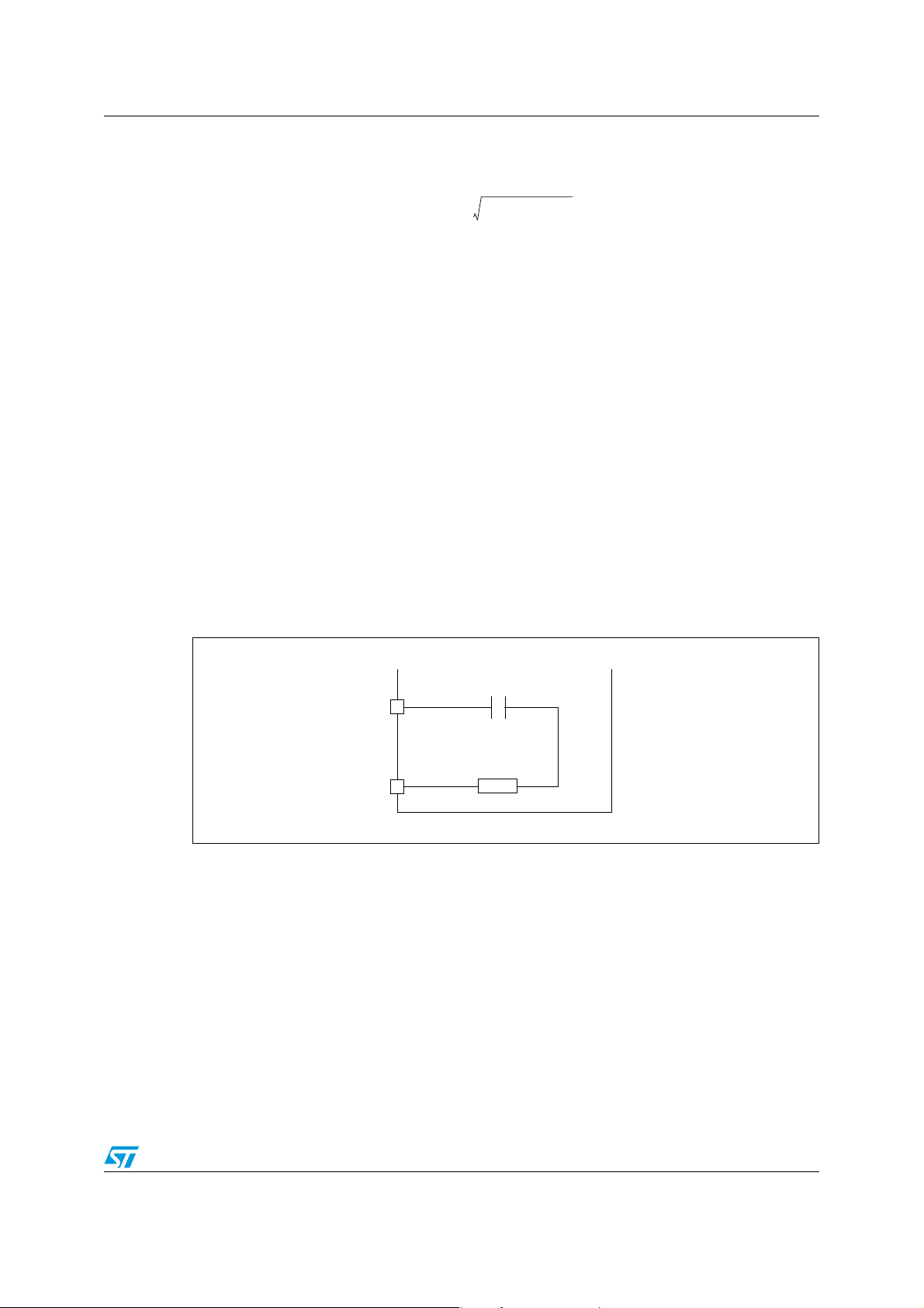
Figure 1. Equivalent Electrical Schematic of an LCD Segment
C
S
Rs
COM
Note: The DC Value should never be more than 100mV (refer to the LCD manufacturer’s
datasheet). Otherwise the life time can be shortened. The frequency range is 30 - 200Hz
typically. If it is less, it flickers; if it is more, the power consumption increases.
3/21
LCD drive signals AN1048
2 LCD drive signals
2.1 Single backplane LCD drive
In a single backplane drive, each LCD segment is connected to a segment line(Sx) and to
one backplane(common line) common to all the segments. A display using S segments is
driven with S+1 MCU output lines. The backplane is driven with a “COM” signal controlled
between 0 and V
When switching a segment “ON”, a signal with opposite polarity to “COM” is sent to the
corresponding “Segment” pin. When the non-inverted signal “COM” is sent to the “Segment”
pin, the segment is “OFF”. Using an MCU, the I/O operates in output mode either at logic 0
or 1.
Figure 2. LCD signals for direct drive
COM
+Vdd
S
+Vdd
with a duty cycle of 50%.
DD
S1=COM-S
+Vdd
S
+Vdd
S1=COM-S
+Vdd
-Vdd
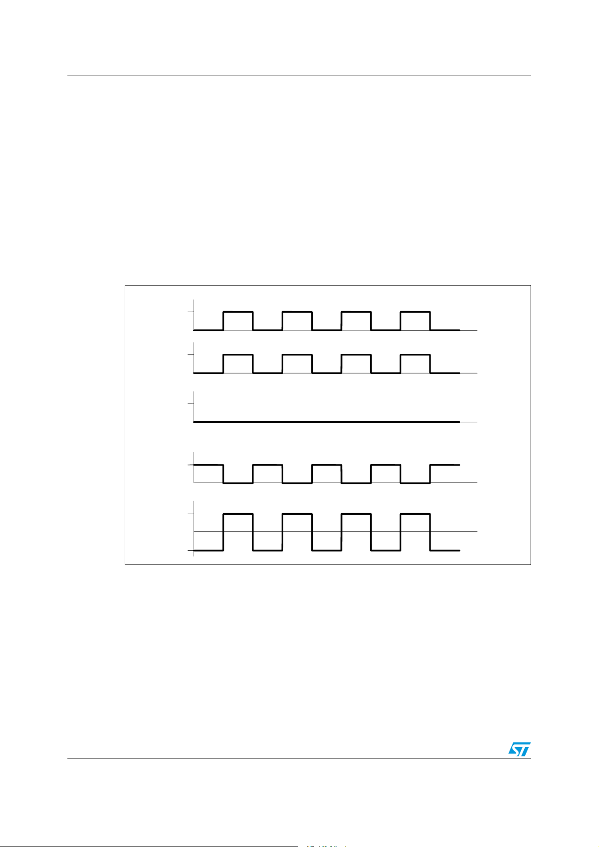
2.2 Duplexed LCD drive
In a duplexed drive, two backplanes are used instead of one. Each LCD segment line(Sx) is
connected to two LCD segments, each one connected on the other side to one of the two
backplanes or common lines(refer to Figure 3). Thus, only (S/2)+2 MCU pins are necessary
to drive an LCD with S segments.
Three different voltage levels have to be generated on the backplanes: 0, V
“Segment” voltage levels are 0 and V
and LCD waveforms. The intermediate voltage V
voltages. The ST7 I/O pins selected as “Backplanes” are set by software to output mode for
O
F
F
O
N
/2 and VDD. The
DD
only. Figure 4 shows typical Backplane, Segment
DD
DD/2 is only required for the Backplane
4/21
AN1048 LCD drive signals
0 or VDD levels and to high impedance input mode for VDD/2. When one backplane is active,
the other one is neutralised by applying V
/2 to it. This VDD/2 voltage is defined by two
DD
resistors of equal value, externally connected to the I/O pin. By using an MCU with flexible
I/O pin configuration, a duplexed LCD drive can be implemented with only 2 external
resistors bridge (each on two com lines).
Figure 3. Basic LCD Segment Connection in duplexed mode
S1
S2 S3
S11 S12
COM1
COM2
Figure 4. LCD signals for duplexed mode (used in the ST7 example)
COM1
+Vdd
+Vdd/2
COM2
+Vdd
+Vdd/2
S1
+Vdd
CASE1 CASE2 CASE3 CASE4
S11=COM1-S1
+Vdd
+Vdd/2
-Vdd/2
-Vdd
SEGMENT1
S12=COM2-S1
+Vdd
+Vdd/2
-Vdd/2
-Vdd
SEGMENT2
OFF ON ONOFF
OFFOFFONON
5/21
LCD drive signals AN1048
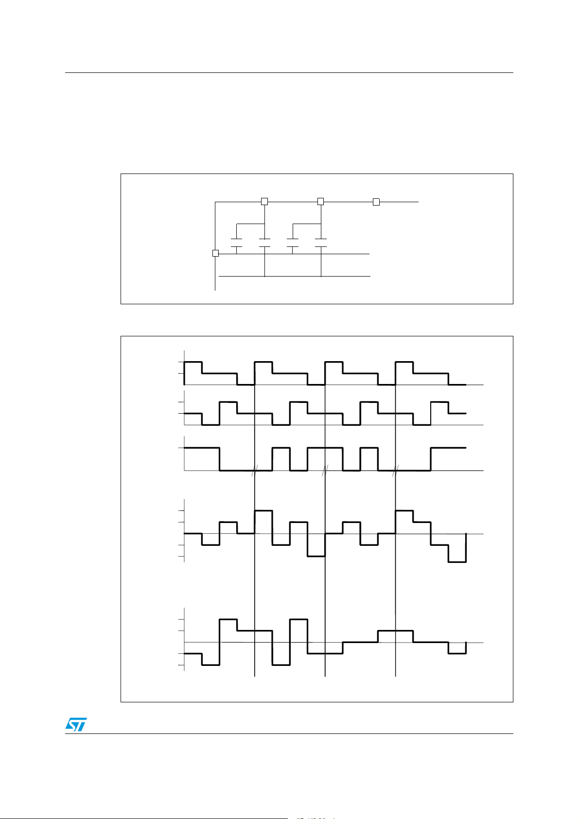
2.3 Quadruplex LCD drive
In a quadruplex LCD drive, four backplanes are used. Each LCD pin is connected to four
LCD segments, with each segment connected on the other side to one of the four
backplanes. Thus, only (S/4)+4 MCU pins are necessary to drive an LCD with S segments.
For example: to drive an LCD with 128 segments (32 x4), only 36 I/O ports are required (32
I/O ports to drive the segments, 4 I/O ports to drive the backplanes).
Three different voltage levels have to be generated on the common lines: 0, V
The Segment line voltage levels are 0 and V
only. The LCD segment is inactive if the
DD
/2, VDD.
DD
RMS voltage is below the LCD threshold voltage and is active if the LCD RMS voltage is
above the threshold. Figure 6 shows typical Backplane, Segment and LCD waveforms. The
intermediate voltage V
selected as “Backplanes” are set by software to output mode for 0 or V
high impedence input mode for V
/2 is only required for Backplane voltages. The MCU I/O pins
DD
/2. The VDD/2 voltage is defined by two resistors of
DD
levels and to the
DD
equal value, externally connected to the I/O pins. When one backplane or COM is active, the
other ones are neutralized by applying V
/2 to them.
DD
Figure 5. Basic LCD Segment Connection in Quadruplexed Mode
COM1
S11
S12
S13
S14
S1
S2
S3
COM2
COM3
COM4
6/21
AN1048 LCD drive signals
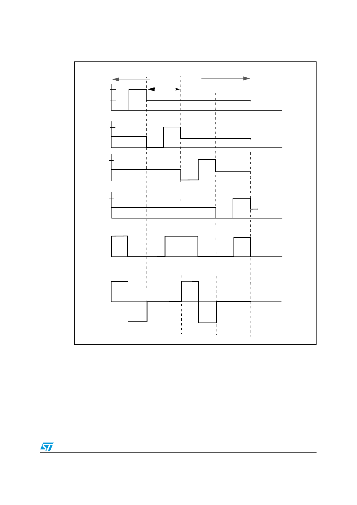
Figure 6. LCD timing diagram for Quadruplex Mode
Single Frame Period
T/4
Control
Period
T/2
3T/8
T
Vcom
Vdd/2
COM1
T/8
COM2
COM3
COM4
Vsegx
Vseg-Vcom
Seg x_1 ON
Vsegx-Vcom1
Segx_2 Off
Segx_3 ON Segx_4 Off
Vsegx-Vcom4
7/21

LCD drive signals AN1048
Figure 7. LCD Timing Diagram for a single segment
Vsegx
Segx
Vsegx
Segx_1 (ON)
Vcom1
Segx_1(off)
2.3.1 LCD mean voltage calculation
The LCD mean voltage must be very close to zero to guarantee long life to the LCD. The LCD mean
voltage for ON and OFF periods can be calculated as:
Vmean(ON) = 1/8 Vseg + 1/8 (-Vcom) + 3(Vseg - Vr/2) + 3(-Vr/2) ----(1)
Vmean(Off) = 3(Vseg/2) + 3(-Vr/2) -----(2)
Vmean(ON) and Vmean(Off) assume identical periods for each phase.
From eqn (1) & (2), to get Vmean(ON) and Vmean(Off) = zero
Vseg = Vcom = Vr = Vcc
Where:
Vcom = Max voltage on COM line
Vr/2 = Voltage in the middle of the resistor bridge applied on the COM line
Vseg = Max voltage on Segx line
Vcc = Microcontroller power supply
8/21

AN1048 LCD drive signals
2.3.2 Contrast calculation
The performance of an LCD driving system is defined by the contrast:
Contrast(D) = Vrms(ON) / Vrms(Off)
For the quadruplex signal as described on the previous page:
T
Vrms ON()
=
1
--- f t()2td
∫
T
0
Vrms ON()
Vrms ON()
Vrms ON()
Vrms ON()0.661Vcc=
Vrms OFF()
=
T
--8
1
---
Vcc()2td
∫
T
0
⎛⎞
1
Vcc()
=
---
⎜⎟
T
⎝⎠
7
Vcc()
-----16
T
--8
1
--- 0()td
∫
T
0
2
2
2T
-------
++=
2T
------8
Vcc()2td
++=
∫
T
--8
2
T
--- Vcc()
8
8
0()td
∫
T
--8
Vcc()
T
-------------------
---
8
T
Vcc
⎛⎞
----------
∫
⎝⎠
2T
------8
T
∫
2T
------8
2
4
2
2
2
Vcc
⎛⎞
----------
⎝⎠
2
6T()8⁄⋅+⋅+⋅
td
td
Vrms OFF()
Vrms OFF()0.43Vcc=
=
Contrast(D) = Vrms(ON) / Vrms(OFF) = 0.661Vcc / 0.43Vcc = 1.52
3
Vcc()
-----16
2
9/21

LCD drive signals AN1048
For comparison, a hardware LCD drive uses 1/3 bias voltage. With 1/3 bias control, the
contrast value (D) is 1.73. Therefore, 1/3 bias gives only a small advantage of contrast
versus temperature. This advantage is reduced to zero when using software contrast
control.
10/21

AN1048 Example of a quadruplex LCD with ST72F321B
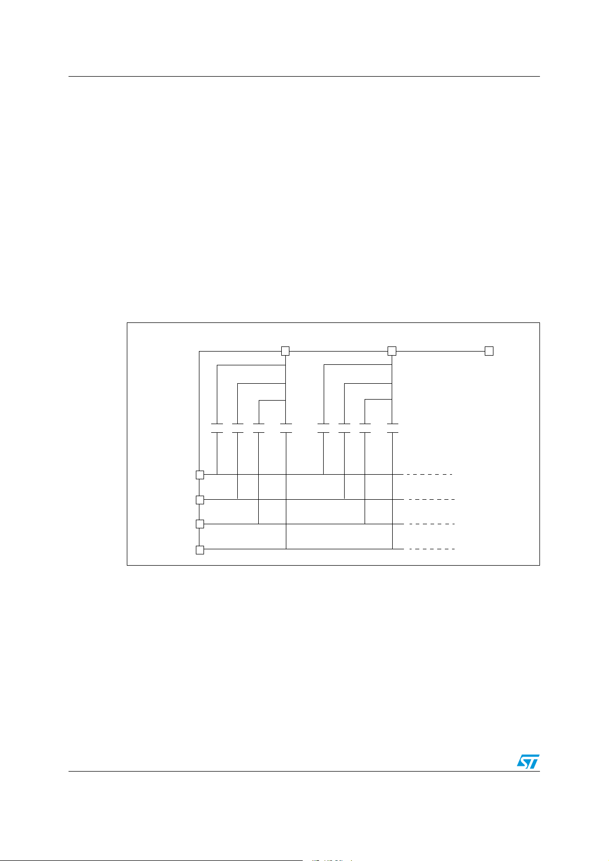
3 Example of a quadruplex LCD with ST72F321B
The following example describes a drive for a quadruplex mode (4COM) LCD using the
ST72F321B (TQFP64 pin package 10 x 10). Refer to Figure 8. The only external
components needed for driving the LCD are eight resistors. The resistor value of 56K is
used to reduce the DC voltage on the LCD(~7.5 mV). This value can be further decreased
to get the better DC voltage on the LCD but this will result in an increase of the current
consumption. One I/O port per segment and one I/O port for each COM line are needed to
drive the LCD. For example: To drive a quadruplex LCD that has 128 segments (with 32
segment lines and 4 COM lines) requires only a total of 36 I/O ports.
In the example program, the Port PA0-A5, PB0-B7, PD0-D7, PF7-F0, PE7-E6 pins are
connected to the 32 segment lines and are used to generate the segment signals. Ports
PC3...PC0 are connected to the 4 COM lines and used to generate the COM signals. The
LCD driver consists of two initialization routines (port init, timer init) and a TimerA interrupt
routine “timer_rt”. To activate the LCD, these two initialization routines have to be called.
After these routines are called, the ST7 gets the timer Output Compare 1 & Output Compare
2 interrupts.
11/21

Example of a quadruplex LCD with ST72F321B AN1048
Figure 8. Hardware Connection Diagram
Vcc
PC0-C3
PA0-A5
PB0-B7
PD0-D7
56K
56K
Network Resistors
Common Lines
LCD GLASS
Segment Lines
6
8
8
PF0-F7
PE6-E7
ST72F321B
The LCD Timing is generated by the TimerA output compare interrupt. Each cycle consists
of four phases, one for each backplane. Each COM line generates its waveform during the
corresponding phase e.g. COM1 line during phase1. During other phases it remains at level
V
/2. Each phase consists of two parts:
DD
1. Active time
2. Dead time
During the Active time, the segment lines and COM lines are used to drive the LCD. During
dead time Segment and COM lines are used to tune the contrast.
12/21
8
2

AN1048 Example of a quadruplex LCD with ST72F321B
Active time starts after the Output Compare 1 interrupt and dead time starts after the Output
Compare 2 interrupt. A total of 16 interrupts are generated in each frame period with four
interrupts per control period. There are 2 Output Compare 1 events (OC1_1 and OC1_2)
and 2 Output Compare 2 events in each phase.These are explained as follows:
During OC1_1, V
is applied to the segments which have to be turned ON and 0 for the
DD
segments which have to be turned OFF. The COM line which corresponds to this phase is
set to low level. Other COM lines are set to level V
DD
/2.
During OC2, all segments and COM lines are inactive (set to low level) if we want to
decrease the Vrms (see Figure 9) and COM lines are set low, segments are set high if we
want to increase the Vrms (see Figure 10).
During OC1_2, Segment Lines are supplied with voltage levels which are inverted to the one
applied during OC1_1.COM line which corresponds to this phase is set to high level.Other
COM lines are set to level V
DD
/2.
Again during OC2, all segments and COM lines are inactive(set to low level) if we want to
decrease the Vrms and COM lines are set high, segments are set low if we want to increase
the Vrms (see Figure 10).
13/21

Example of a quadruplex LCD with ST72F321B AN1048
Figure 9. LCD timing diagram with Dead & Active Time (to decrease Vrms)
dead time
control
period
Vcom
Vdd/2
COM1
Vcom
Vdd/2
COM2
Vcom
Vdd/2
COM3
Vcom
Vdd/2
COM4
Vseg
Segx
(ON)
active
time
T/4 T/2 3T/4 T
Vseg
Vdd/2
Segx_1
On
Vcom
Vdd/2
Segx_1
Off
oc1_1
OC2
OC1_2
OC2
oc1_1
14/21

AN1048 Example of a quadruplex LCD with ST72F321B
Figure 10. LCD timing diagram with Active and dead time (to increase Vrms)
Dead time
Period
COM1
ActiveControl
time
COM2
COM3
COM4
Vseg
Segx
(ON)
Vseg
Vdd/2
Segx_1
(ON)
T/ 4
T/2
3T/4
T
Vseg
Vdd/2
Segx_1
(Off)
oc1_1
oc2
oc1_2
oc2
15/21

Software contrast control AN1048
4 Software contrast control
The software contrast control is under pending patent from STMicroelectronics. The use of
this technique with a non-STMicroelectronics' Microcontroller has to be agreed by
STMicroelectronics.
The LCD contrast is controlled entirely by software without the use of any external
components. LCD contrast can be adjusted to the optimal value depending on the operating
voltage of the LCD used. The LCD contrast is controlled by varying the timing of dead phase
as shown in the LCD timing diagram.
Deadtime can be used to decrease as well as to increase the Vrms of the LCD. Deadtime is
the voltage compensation time to regulate rms voltage up and down. Dead time can be
implemented either after each control period or at the end of the frame. To avoid flickering,
the duration of the dead time must be adjusted depending on the quality of LCD and the
frequency of the frame.
In the example in Figure 9, the Rms value of the LCD decreases if the duration of dead time
is increased and Rms value increases if the duration of dead time decreases. In Figure 10,
this works the opposite way.
4.1 Contrast calculations
Let the frame period = T + xT
where T - Active Time, xT- Dead Time
x- Proportion of dead time, Vx - Voltage during the dead time
TXT+()
1
Vrms ON()
Vrms ON()
Vrms ON()
=
=
=
---------------- TxT+
---------------- -
TxT+
1
---------------- TxT+
∫
1
ft()2td
0
T
⎛⎞
---
⎜⎟
8
Vcc()2tVcc–()2tVcc()2⁄()2tVx
⎜⎟
∫
⎜⎟
0
⎝⎠
⎛⎞
2
Vcc()
⎜⎟
⎝⎠
T
--- Vcc()
8
2T
-------
8
+d
∫
T
---
8
2
T
---
8
T
+d
∫
2T
------ -
8
Vcc()
------------------ -
4
2
2T
------ - Vx
8
xT
------ -
8
2
()t8⋅d
+d
∫
0
2
xT
⎛⎞
------ -
⋅
⎝⎠
8⋅+⋅+⋅+⋅
8
16/21

AN1048 Software contrast control
Vrms ON()
=
⎛⎞
()
1
------------
------------------------- - Vx()2x⋅+
⎜⎟
1x+
⎝⎠
14V cc
32
2
Since Vx = 0 (incase of a decrease in Vrms)
2
14V cc
()
1
------------
Vrms ON()
=
Vrms ON()
Vrms OFF()
1x+
1
-----------1x+
=
-------------------------32
0.661V cc=
T
---
⎛⎞
1
8
⎜⎟
---------------- -
TxT+
0()t0()tVcc()2⁄()
∫
⎜⎟
0
⎝⎠
2T
-------
8
+d
∫
T
---
8
T
+d
∫
2T
-------
8
xT
------ -
8
2
tVx
()t8⋅d
+d
∫
0
2
2
6Vcc
()
---------------------- Vx2x⋅+
32
Vrms OFF()
=
⎛⎞
1
------------
⎜⎟
1x+
⎝⎠
Since Vx = 0 (incase of a decrease in Vrms)
Vrms OFF()
Contrast Dx()
1
0.18Vcc=
-----------1x+
1
⎛⎞
⎝⎠
-------------------------------------------------=
0.661V cc
-----------1x+
1
⎛⎞
⎝⎠
-----------1x+
0.18Vcc
Where Dx = Contrast calculation with contrast control method
17/21

LCD demo board AN1048
The contrast D, between VON and V
optical contrast by tuning V
ON
5 LCD demo board
5.1 Schematic
PF7
PF5
PF3
PD1
PB7
PB5
PB3
PB1
PF6
PD0
PB6
PB4
PB2
PB0
S1
SW-PB
7k
R5
4.
RESET
C12
22pf
hz
16M
C11
22pf
OSCINOSC2
10µ F
+5
2
1
HEADER
PF1
PE7
PA5
PA3
PA1
VIM878-DP6.35-RH-W-HV
101112131415161718 19
PF4
PF2
PF0
PE6
PA4
PA2
PA0
C13
100nF
GND
PA4
4
9
PA5
5
0
5
1
5
2
VPP
5
3
RESET
5
4
5
5
5
6
7
5
OSC2
5
8
OSC1
5
9
6
0
6
1
6
2
6
3
6
4
PC0
PC1
2021222324252627282930313233343536
PC3
PC2
U1
PD7
PD5
PD3
U2
123456789
PD6
PD4
PD2
+5
Y1
C6
C1 100nF
+5
JP1
2
is constant (quality of contrast). We only change the
OFF
close to the threshold value of the LCD.
+5
123
4
J1
SO
I
PC5
M
SS
SCK
OSI
M
100nF
C3
10µ F+5 +5
F
10µ
C2
100nF
100nF
C4
F
C9
10µ
PA4
PA5
VPP
RESET
EVD
TLI
VSS2
OSC2
OSC1
VDD2
PE2
PE3
+5
48
VSS1
PA6/ SD A
PA7 / SCL I
PE0/ TD O
PE1/R DI
4
PE
1
3
2
1
J2
PA3
PA2
PA1
PA0
PC7
42
46
47
PA043PA144PA245PA3
VDD1
SS/AIN15
PC7/
ST72321B
PE52PE63PE74PB0/PWM35PB1/PWM26PB2/PWM17PB3/PWM08PB4/ARTCLK9PB5/ARTIC1
PE6
PE7
PB0
PB1
PB2
OSCIN
PC6
41
PC6/SCK/ICCCLK
PB3
OSC1
R6
R1
R2
PC5
PC4
39
40
/AIN14
OSI
M
PC5/
10
PB4
PB5
JP2
10K
R7
+5
10k
10K
+5
7K
4.
PC3
PC2
PC1
36
37
38
CAP2-B
CAP1-B
I
I
ICCDATA
PC2/
PC3/
PC4/M ISO/
PB6/ARTIC211PB712PD0/AINO13PD1/AIN114PD2/AIN215PD3/AIN3
PB6
PB7
PD0
1234
5678910
CC
I
R4
4.7K
7K
R3
VPP
RESET
PC6
PC4
R11
56K
R10
56K
56K
R9
56K
R8
PC3
+5
100nF
C5
F
C10
10µ
PC0
33
34
VSS0
VDD0
PC0/OCMP2-B/AIN1235PC1/OCMP1-B/AIN13
A
16
PD1
PD2
PD3
4.
56K
PORT C
R15
56K
R14
56K
56K
R13
R12
56K
PC0
PC1
PC2
PF7/E X TC L K -A
7
PF
2
3
PF6/IC AP1-A
PF6
3
1
PF5/AI N11/ ICA P2-A
PF5
0
3
PF4/AI N10/ OCMP1-
PF4
9
2
PF3/A I N 9/ OC M P2- A
PF3
2
8
PF2
PF2
7
2
PF1/B EE P
PF0/A I N 8/ M CO
VSS3
VDD3
VSSA
VAREF
PD7/ A I N7
PD6/ A I N6
PD5/ A I N5
PD4/ A I N4
C8
1
PF
6
2
PF0
2
5
24
3
2
2
2
1
2
PD7
2
0
PD6
9
1
C7
PD5
1
8
PD4
7
1
SPI
18/21

AN1048 LCD demo board
5.2 Power supply
The LCD demo board should be supplied by a maximum DC voltage of 5V. The board is
provided with the connector JP1 for this board supply.
Note: For the demo software loaded inside the micro, the board should be supplied with 5V. The
software attached to this application note displays the word “EMBEDDED” and tunes
automatically its contrast from transparent to dark with the ST software pattented method.
The Vrms increase is performed by putting the segment voltage once at Vdd, once at -Vdd
during the dead times, the Vrms decrease is performed by putting at 0 the segment voltage
during the same dead times. The voltage average is then kept. Refer to the software
attached to this application note for more details.
5.3 Programming
The demo board uses the ST72F321B microcontroller and can be programmed using the
ICC protocol. The board is provided with the ICC connnector JP2. By default, OSC_TYP is
programmed as a resonator oscillator in the option bytes. You can disable the option bytes
when you want to use the ICC clock to program the micro.
5.4 Reset
The device can be reset by pressing the switch s1 on the demo board.
5.5 Oscillation system
The demo board is mounted with a 16 MHz crystal with 8 MHz fcpu. You can change this
clock value but need to modify the timer setting inside the software accordingly.
19/21

Revision history AN1048
6 Revision history
Table 1. Document revision history
Date Revision Changes
Document reformatted
References to ST72F321 changed to ST72F321B
09-May-2006 5
Formulae for VRMS(ON) and VRMS(OFF) corrected, Section 4.1 on
page 16
Note updated, Section 5.2 on page 19
20/21

AN1048
Please Read Carefully:
Information in this document is provided solely in connection with ST products. STMicroelectronics NV and its subsidiaries (“ST”) reserve the
right to make changes, corrections, modifications or improvements, to this document, and the products and services described herein at any
time, without notice.
All ST products are sold pursuant to ST’s terms and conditions of sale.
Purchasers are solely responsible for the choice, selection and use of the ST products and services described herein, and ST assumes no
liability whatsoever relating to the choice, selection or use of the ST products and services described herein.
No license, express or implied, by estoppel or otherwise, to any intellectual property rights is granted under this document. If any part of this
document refers to any third party products or services it shall not be deemed a license grant by ST for the use of such third party products
or services, or any intellectual property contained therein or considered as a warranty covering the use in any manner whatsoever of such
third party products or services or any intellectual property contained therein.
UNLESS OTHERWISE SET FORTH IN ST’S TERMS AND CONDITIONS OF SALE ST DISCLAIMS ANY EXPRESS OR IMPLIED
WARRANTY WITH RESPECT TO THE USE AND/OR SALE OF ST PRODUCTS INCLUDING WITHOUT LIMITATION IMPLIED
WARRANTIES OF MERCHANTABILITY, FITNESS FOR A PARTICULAR PURPOSE (AND THEIR EQUIVALENTS UNDER THE LAWS
OF ANY JURISDICTION), OR INFRINGEMENT OF ANY PATENT, COPYRIGHT OR OTHER INTELLECTUAL PROPERTY RIGHT.
UNLESS EXPRESSLY APPROVED IN WRITING BY AN AUTHORIZE REPRESENTATIVE OF ST, ST PRODUCTS ARE NOT DESIGNED,
AUTHORIZED OR WARRANTED FOR USE IN MILITARY, AIR CRAFT, SPACE, LIFE SAVING, OR LIFE SUSTAINING APPLICATIONS,
NOR IN PRODUCTS OR SYSTEMS, WHERE FAILURE OR MALFUNCTION MAY RESULT IN PERSONAL INJURY, DEATH, OR
SEVERE PROPERTY OR ENVIRONMENTAL DAMAGE.
Resale of ST products with provisions different from the statements and/or technical features set forth in this document shall immediately void
any warranty granted by ST for the ST product or service described herein and shall not create or extend in any manner whatsoever, any
liability of ST.
ST and the ST logo are trademarks or registered trademarks of ST in various countries.
Information in this document supersedes and replaces all information previously supplied.
The ST logo is a registered trademark of STMicroelectronics. All other names are the property of their respective owners.
© 2006 STMicroelectronics - All rights reserved
STMicroelectronics group of companies
Australia - Belgium - Brazil - Canada - China - Czech Republic - Finland - France - Germany - Hong Kong - India - Israel - Italy - Japan -
Malaysia - Malta - Morocco - Singapore - Spain - Sweden - Switzerland - United Kingdom - United States of America
www.st.com
21/21
 Loading...