

Page 1

AN1042
APPLICATION NOTE
ST7 ROUTINE FOR I2C SLAVE MODE MANAGEMENT
by Microcontroller Division Application Team
INTRODUCTION
The goal of this appli cation note is to pres ent a usefu l example of com municati on using the
I2C peripheral of the ST7. The ST7 microcontroller is used as a slave an d can com municate
with any master. This slave, through the I2C interface, receives data bytes from the master implement ing er ror ma nage ment and re turns the m. This app licatio n has been r ealiz ed wi th a
ST72264,7-bit, general call and 10-bit addressing mode.
1 ST7 I2C INT ERFACE
The ST7 I2C peripheral allows multi master and slave communication with bus error management. In this application, only the single slave mode is used (with error management).
The I2C synchronous communication needs only two signals: SCL (Serial clock line) and SDA
(Serial data line). The corresponding por t pins have to be configured as floating inputs ( here
PA4 and PA6).
Please refer to the ST7 datasheet for more details.
1.1 COMMUNICATION SPEED
The ST7 I2 C peripher al allows to communi cate at diff erent spe eds. It is able to work in
standard and fast I2C modes up to 400kHz.
It’s the master which imposes the communication speed. For more details, please refer to the
AN971.
1.2 START, STOP CONDITION AND ACKNOWLEDGE GENERATION
The Start and Stop conditions are sent by the master.
An Acknowledge is sent after an address or a data byte is received when the ACK bit is set in
the Control register (CR).
AN1042/0803 1/8
1
Page 2
ST7 ROUTINE FOR I2C SLAVE MODE MANAGEMENT
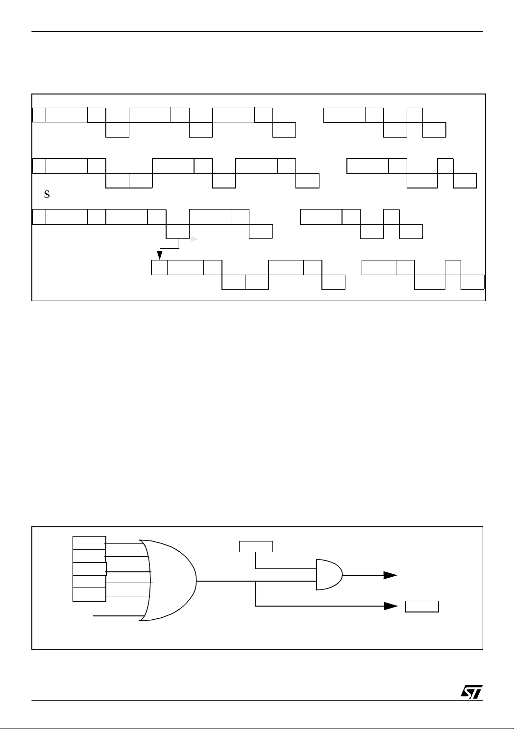
1.3 TRANSFER SEQUENCING Figure 1. I2C Slave Transfer Sequencing Diagram
7-bit Slave receiver:
S Address A Data1 A Data2 A
EV1 EV2 EV2 EV2 EV4
7-bit Slave transmitter:
S Address A Data1 A Data2 A
EV1 EV3 EV3 EV3 EV3-1 EV4
S
10-bit Slave receiver:
S HeaderAAddress A Data1 A
EV1 EV2 EV2 EV4
10-bit Slave transmitter:
SrHeader A Data1 A
EV1 EV3 EV3 EV3-1 EV4
.....
DataN A P
.....
DataN NA P
.....
DataN A P
DataN AP
....
.
Legend:S=Start, P=Stop, A=Acknowledge, NA=Non-Acknowledg e, EVx=Even t (with interruptif ITE=1).
EV1: EVF=1, ADSL=1, cleared by rea ding SR1 r egister.
EV2: EVF=1, BTF=1, cleared by reading SR1 register followed by reading DR register.
EV3: EVF=1, BTF=1, cleared by reading SR1 register followed by writing DR register.
EV3_1: EVF=1, AF=1, cleared by reading SR1 register.
EV4: EVF=1, STOPF=1, cleared by reading SR2 register.
In blue are events sent by the master whereas blank ones are events sent by the slave.
These frames are sequential and as the SDA l ine is bidirectional, this line is held sometimes
by the master and sometimes by the slave.
1.4 SLAVE EVENT FLAGS AND INTERRUPT GENERATION Figure 2. Slave Interrupt Events Diagram
BTF
AF
ADSL
STOPF
BERR
*
*
EVF can also be set by EV6 or an error fro m the SR2 regis ter.
ITE
INTERRUPT
EVF
2/8
2
Page 3
ST7 ROUTINE FOR I2C SLAVE MODE MANAGEMENT
2 ST7 I2C COMMUNICATION APPLICATIO N
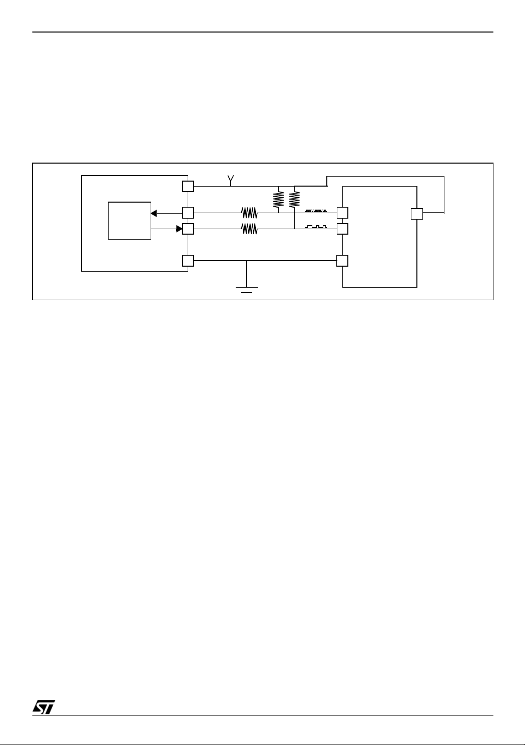
2.1 HARDWARE CONFIGURATION
The ST7 I2C communication application hardware is composed by a ST72264 microcontroller
used as a slave which communicates with any master through an I2C bus interface.
Figure 3. ST7 I2C Communication Application
5V
SCL
SDA
Vdd
2x100Ω
2x27KΩ
master
SCL
SDA
Vdd
ST72F264
I2C
Vss
Vss
2.2 ST7 I2C PERIPHERAL BASIC DRIVERS
In this chapter all registers refer to the ST7 I2C peripheral ones (otherwise specified).
2.2.1 Initialize the I2C peripheral
In this application the initialization of the ST7 I2C peripheral is done completely by software.
First the Control register (CR) is cleared and the Data (DR) and Status (SR1,SR 2) registers
are touched to clear all possible pending event.
Then, the peripheral is enabled thr ough the C ontrol register (CR ). This action ne eds to wr ite
twice in the register due to the fact that the Control r egister (CR) bits can be set onl y when the
PE enab le bi t is alre ady set. To allow the pe riph eral to ack nowl edge th e re ceive d dat a the
ACK bit of the Control register (CR) is set.
2.2.2 Slave Communication on the I2C Bu s
First the interface frequency must be configured using the FRi bits in the OAR2 register.For
10 bit addressing mode, user must configure the slave address using the ADD9 and ADD8
bits of the OAR2 register.
To initiate a I2C com mu nication, fir st a start c onditi on has to be ge nerated an d then the se lected slave address has to be sent, both by the mas ter. As soon as a start condition is detected, the address is received from the SDA line and sent to the shift register; then it is compared with the address of the interface (OAR1) or the General Call address (if selected by software). If the GCAL option is to be implemented, user must enable it by selecting the
GCAL_Add in user customizable part of the code.
3/8
Page 4

ST7 ROUTINE FOR I2C SLAVE MODE MANAGEMENT
When the address received matches, the interface generates in sequence:
- Acknowledge pulse if the ACK bit is set.
- EVF and ADSL are set with an interrupt if ITE bit is set.
Then the inte rface waits for a read of SR 1 regis ter, holdi ng the SCL line low. The n it deter-
mines from the TRA bit of the SR1 register if the slave has to be receiver or transmitter.
- TRA = 0: Data byte received (if BTF=1)
- TRA=1: Data byte transmitted
2.2.3 Receiving Data on the I2C Bus
The slave then receives bytes from the SDA line into the DR register via the internal shift interface. After each byte, the interface generates in sequence:
- Acknowledge pulse if the ACK bit is set.
- EVF and BTF bits are set with an interrupt if ITE bit is set.
Then the interface waits f or a read of the S R1 regi ster followed b y a read of the DR register
(see Transfer Sequencing).
After each reception, the data bytes received are placed in a table. If a n error occurs, the in-
terface is re-i nitiali zed (I2CCR cl eared and put to its initi al value after having removed pending
interrupts) and the slave waits for next start condition.
2.2.4 Sending Data on the I2C Bu s
When the slave receives start condition and m atching slave address (w ith LSB set) from the
master, it become s tra nsmitter a nd t hen sends the m aster back data it stored into a tab le. It
sends data from DR register to the SDA line via the internal shift register.
The slave waits for a read of the SR1 register followed by a write of next data into the DR register (see Transfer Sequencing).
When the acknowledge pulse is received:
- the EVF and BTF bits are set by hardware with an interrupt if ITE bit is set.
After the last data byte is transferred, a Stop condition is generated by the master. The inter-
face detects this condition and sets:
- EVF and STOPF bits with an interrupt if ITE bit is set.
Then the interface waits for a read of the SR2 register.
In this application, the TRA bit of the SR1 register is used as a fl ag to deter mine the mode (re-
ceiver or transmitter) of the microcontroller.
4/8
Page 5
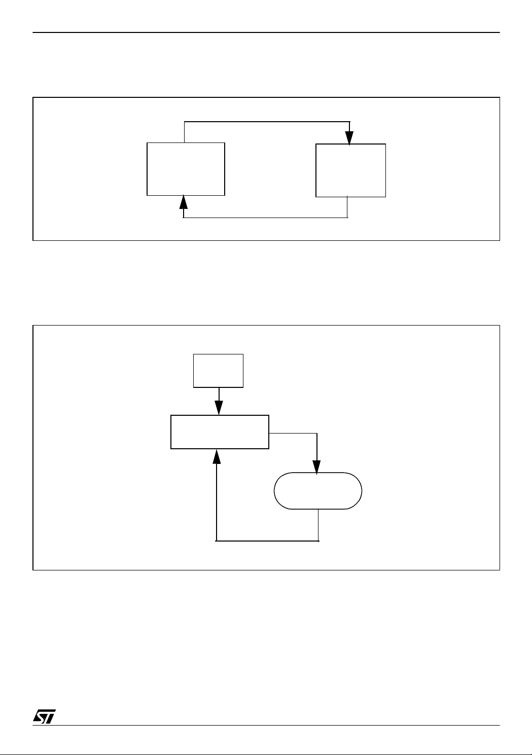
2.3 COMMUNICATION Figure 4. Communication Flow
ST7 ROUTINE FOR I2C SLAVE MODE MANAGEMENT
3 data bytes
MASTER
SLAVE
3 data bytes
The ST7 slave mode management application is based on two steps driven by the master:
– a reception of 3 data bytes from any master.
– a transmission of received data bytes to the master.
Figure 5. Main Program Flowchart
Init
Infinite loop
Interrupt
Events in the following flowchart refer to events defined into the paragraph “Transfer sequencing” on page 2.
5/8
Page 6

ST7 ROUTINE FOR I2C SLAVE MODE MANAGEMENT
Figure 6. Interrupt Flowchart
I2CST1=I2CSR1
I2CST2=I2CSR2
reset of the
I2C ce ll
no
no
yes
error?
no
EV1?
no
EV2?
EV4?
EV4
(stop)
yes
yes
yes
reset I2C
EXIT
TRA=1
yes
EV3
(transmitter)
no
EXIT
EV2
(receiver)
EXIT
6/8
EXIT
EXIT
Page 7

ST7 ROUTINE FOR I2C SLAVE MODE MANAGEMENT
3 SOFTWARE
All the source files in assembly code are given in the zip file with this application note.
The source files are for guidance only. STMicroelectronics shall not be held liable for any di-
rect, indirect or consequential damages with respect to any claims arising from use of this s oftware.
7/8
Page 8

ST7 ROUTINE FOR I2C SLAVE MODE MANAGEMENT
THE PRESENT NOTE WHICH IS FOR GUIDANCE ONLY AIMS AT PROVIDING CUSTOMERS WITH INFORMATION
REGARDING THE IR PRO DUCT S IN OR DER FO R THEM TO SAV E TIME . AS A RES ULT, STMIC ROEL ECTR ONI CS
SHALL NOT BE HELD LIABLE FOR ANY DIRECT, INDIRECT OR CONSEQUENTIAL DAMAGES WITH RESPECT TO
ANY CL AIM S AR IS IN G FR OM T HE CO N TENT OF S UC H A NO TE A ND /O R T HE U SE M AD E BY C US TO ME RS O F
THE INFORMATION CONTAINED HEREIN IN CONNECTION WITH THEIR PRODUCTS.
Information furnished is believed to be accurate and reliable. However, STMicroelectronics assumes no responsibility for the consequences
of use of such information nor for any infringement of patents or other rights of third parties which may result from its use. No license is granted
by implic ation or otherwise under any patent or patent r i ght s of STMi croelectr oni cs. Spec i fications mentioned i n this publication are subject
to change without notice. This publication supersedes and replaces all information previously supplied. STMicroelectronics product s are not
authorized for use as cri tical comp onents in lif e support devi ces or systems without the express written appr oval of STMic roelectronics.
The ST logo is a registered trademark of STMicroelectronics
2003 STMicroelectronics - All Rights Reserved.
STMicroelectronics Group of Compan i es
http://www.s t. com
Purchase of I
2
C Components by STMicroelectronics conveys a license under the Philips I2C Patent. Rights to use the se components in an
2
I
C system i s granted pro vi ded that the sy stem conforms to the I2C Standard Specification as defined by Philips.
Australi a - B razil - Canada - China - Finl and - Franc e - Germany - Hong Kong - Ind i a - Is rael - Ital y - J apan
Malaysi a - M al ta - Morocco - Singapore - Spain - Sw eden - Switzerland - Uni ted Kingdom - U.S.A.
8/8
 Loading...