


AN1014
APPLICATION NOTE
HOW TO MINIMIZE THE ST7 POWER CONSUMPTION
By MCD Application Team
1 INTRODUCTION
The purpose of this document is to explain the different low power modes available on ST7 devices and the ways to minimise power consumption. Many applications will have strict power
requirements, and there are several me thods of lowering the rate of po wer consumpti on
without sacrificing perform ance. Calculati ng the predicted power use is imp ortant to characterize the system ’s power supp ly requirem ents. T he ST7 can be put into one of se veral low
power modes by setting some bits in some registers. The utility of these low power modes depends on the specific application.
The basic explanation of this note is based on ST72F324, but is applicable to all ST7 general
purpose devices. P lease refer s ec tion “Ex amples” to s ee more i nformat ion on additio nal devices (ST7FLITE0).
2 POWER CONSUMPTION FACTO RS
CMOS digital logic device power consumption is affected by supply voltage and clock frequency. These parameters can be adjusted to realize power savings, and are readily controlled by the designer. In CMOS digital logic devices, powe r consumption is directly proportional to clock frequency and power supply squared.
power = CV2f
where: C is CMOS load capacitance, V is supply voltage, and f is clock frequency.
The amount of current used in CMOS logic is directly proportional to the voltage of the power
supply. Thus, power consumption may be reduced by lowering the supply voltage to the device. Power consu mption depends on the num ber of active peripherals. The greater the
number of active peripherals, the more power will be consumed. Power consumption also depends on, whether the oscillator is On or Off and whether the CPU is On or Off. It also depends
on PLL On/Off, CSS enabled/disabled and LVD On/Off.
Power Consumption is based on which mode a particular application is running. For example,
in ST7, “HALT” mode is the lowest power consumption mode without availability of Real Time
Clock and “ACTIVE-HALT” mode is the low est power consumption mode with Real Time
Clock available. To reduce the power consumption, clock frequency can be reduced whenever
fast processing is not required by the application.
AN1014/0603 1/25
1

HOW TO MINIMIZE THE ST7 POWER CONSUMPTION
1 INTRODUCTION . . . . . . . . . . . . . . . . . . . . . . . . . . . . . . . . . . . . . . . . . . . . . . . . . . . . . . 1
2 POWER CONSUMPTION FACTORS . . . . . . . . . . . . . . . . . . . . . . . . . . . . . . . . . . . . . 1
3 POWER MANAGEMENT MODES . . . . . . . . . . . . . . . . . . . . . . . . . . . . . . . . . . . . . . . . 4
3.1 STANDARD RUN MODE . . . . . . . . . . . . . . . . . . . . . . . . . . . . . . . . . . . . . . . . . . . 4
3.2 SLOW MODE . . . . . . . . . . . . . . . . . . . . . . . . . . . . . . . . . . . . . . . . . . . . . . . . . . . . 4
3.3 WAIT MODE . . . . . . . . . . . . . . . . . . . . . . . . . . . . . . . . . . . . . . . . . . . . . . . . . . . . . 4
3.4 SLOW WAIT MODE . . . . . . . . . . . . . . . . . . . . . . . . . . . . . . . . . . . . . . . . . . . . . . . 5
3.5 ACTIVE-HALT MODE . . . . . . . . . . . . . . . . . . . . . . . . . . . . . . . . . . . . . . . . . . . . . 5
3.6 HALT MODE . . . . . . . . . . . . . . . . . . . . . . . . . . . . . . . . . . . . . . . . . . . . . . . . . . . . . 5
3.7 SUMMARY . . . . . . . . . . . . . . . . . . . . . . . . . . . . . . . . . . . . . . . . . . . . . . . . . . . . . . 6
4 EXAMPLES . . . . . . . . . . . . . . . . . . . . . . . . . . . . . . . . . . . . . . . . . . . . . . . . . . . . . . . . . . 6
5 POWER MANAGEMENT TIPS . . . . . . . . . . . . . . . . . . . . . . . . . . . . . . . . . . . . . . . . . . . 6
6 APPENDIX A: ST72F324 STANDARD EXAMPLES . . . . . . . . . . . . . . . . . . . . . . . . . . 7
6.1 EXAMPLE 1: STATIC M EASUREME NT . . . . . . . . . . . . . . . . . . . . . . . . . . . . . . . 7
6.1.1 Measurement Configuration . . . . . . . . . . . . . . . . . . . . . . . . . . . . . . . . . . . . . . . . . . . . 7
6.1.2 Consumption . . . . . . . . . . . . . . . . . . . . . . . . . . . . . . . . . . . . . . . . . . . . . . . . . . . . . . . 7
6.1.2.1 Run Mode . . . . . . . . . . . . . . . . . . . . . . . . . . . . . . . . . . . . . . . . . . . . 7
6.1.2.2 Slow Mode . . . . . . . . . . . . . . . . . . . . . . . . . . . . . . . . . . . . . . . . . . . 8
6.1.2.3 Wait Mode . . . . . . . . . . . . . . . . . . . . . . . . . . . . . . . . . . . . . . . . . . . 8
6.1.2.4 Slow-Wait Mode . . . . . . . . . . . . . . . . . . . . . . . . . . . . . . . . . . . . . . . 9
6.1.2.5 Active-Halt Mode . . . . . . . . . . . . . . . . . . . . . . . . . . . . . . . . . . . . . 10
6.1.2.6 Halt Mode . . . . . . . . . . . . . . . . . . . . . . . . . . . . . . . . . . . . . . . . . . . 10
6.1.3 Conclusion . . . . . . . . . . . . . . . . . . . . . . . . . . . . . . . . . . . . . . . . . . . . . . . . . . . . . . . . 10
6.2 EXA MPLE 2: APPLICATIO N WITH PERIODIC WAKE-UP . . . . . . . . . . . . . . . 11
6.2.1 Measurement Configuration . . . . . . . . . . . . . . . . . . . . . . . . . . . . . . . . . . . . . . . . . . . 11
6.2.2 Consumption . . . . . . . . . . . . . . . . . . . . . . . . . . . . . . . . . . . . . . . . . . . . . . . . . . . . . . 11
6.2.2.1 Wait Mode . . . . . . . . . . . . . . . . . . . . . . . . . . . . . . . . . . . . . . . . . . 12
6.2.2.2 Slow-Wait Mode . . . . . . . . . . . . . . . . . . . . . . . . . . . . . . . . . . . . . . 12
6.2.2.3 Halt Mode . . . . . . . . . . . . . . . . . . . . . . . . . . . . . . . . . . . . . . . . . . . 13
6.2.3 Conclusion . . . . . . . . . . . . . . . . . . . . . . . . . . . . . . . . . . . . . . . . . . . . . . . . . . . . . . . . 13
6.3 EXAMPLE 3: APPLICATION WITH PERIODIC WAKEUP AND WATCHDOG 13
6.3.1 Measurement Configuration . . . . . . . . . . . . . . . . . . . . . . . . . . . . . . . . . . . . . . . . . . . 14
2/25
2

HOW TO MINIMIZE THE ST7 POWER CONSUMPTION
6.3.2 Application . . . . . . . . . . . . . . . . . . . . . . . . . . . . . . . . . . . . . . . . . . . . . . . . . . . . . . . . 15
6.3.3 Conclusion . . . . . . . . . . . . . . . . . . . . . . . . . . . . . . . . . . . . . . . . . . . . . . . . . . . . . . . . 15
7 APPENDIX B: ST7FLITE0 STANDARD EXAMPLES . . . . . . . . . . . . . . . . . . . . . . . . 16
7.1 EXAMPLE 1: STATIC M EASUREME NT . . . . . . . . . . . . . . . . . . . . . . . . . . . . . . 16
7.1.1 Measurement Configuration . . . . . . . . . . . . . . . . . . . . . . . . . . . . . . . . . . . . . . . . . . . 16
7.1.2 Consumption . . . . . . . . . . . . . . . . . . . . . . . . . . . . . . . . . . . . . . . . . . . . . . . . . . . . . . 16
7.1.2.1 Run Mode . . . . . . . . . . . . . . . . . . . . . . . . . . . . . . . . . . . . . . . . . . . 17
7.1.2.2 Slow Mode . . . . . . . . . . . . . . . . . . . . . . . . . . . . . . . . . . . . . . . . . . 17
7.1.2.3 Wait Mode . . . . . . . . . . . . . . . . . . . . . . . . . . . . . . . . . . . . . . . . . . 18
7.1.2.4 Slow-Wait Mode . . . . . . . . . . . . . . . . . . . . . . . . . . . . . . . . . . . . . . 18
7.1.2.5 Active-Halt Mode . . . . . . . . . . . . . . . . . . . . . . . . . . . . . . . . . . . . . 19
7.1.2.6 Halt Mode . . . . . . . . . . . . . . . . . . . . . . . . . . . . . . . . . . . . . . . . . . . 19
7.1.3 Conclusion . . . . . . . . . . . . . . . . . . . . . . . . . . . . . . . . . . . . . . . . . . . . . . . . . . . . . . . . 19
7.2 EXA MPLE 2: APPLICATIO N WITH PERIODIC WAKE-UP . . . . . . . . . . . . . . . 19
7.2.1 Measurement Configuration . . . . . . . . . . . . . . . . . . . . . . . . . . . . . . . . . . . . . . . . . . . 20
7.2.2 Consumption . . . . . . . . . . . . . . . . . . . . . . . . . . . . . . . . . . . . . . . . . . . . . . . . . . . . . . 20
7.2.2.1 Wait Mode . . . . . . . . . . . . . . . . . . . . . . . . . . . . . . . . . . . . . . . . . . 20
7.2.2.2 Slow-Wait Mode . . . . . . . . . . . . . . . . . . . . . . . . . . . . . . . . . . . . . . 21
7.2.2.3 Halt Mode . . . . . . . . . . . . . . . . . . . . . . . . . . . . . . . . . . . . . . . . . . . 21
7.2.3 Conclusion . . . . . . . . . . . . . . . . . . . . . . . . . . . . . . . . . . . . . . . . . . . . . . . . . . . . . . . . 22
7.3 EXAMPLE 3: APPLICATION WITH PERIODIC WAKEUP AND WATCHDOG 22
7.3.1 Measurement Configuration . . . . . . . . . . . . . . . . . . . . . . . . . . . . . . . . . . . . . . . . . . . 22
7.3.2 Application . . . . . . . . . . . . . . . . . . . . . . . . . . . . . . . . . . . . . . . . . . . . . . . . . . . . . . . . 23
7.3.3 Conclusion . . . . . . . . . . . . . . . . . . . . . . . . . . . . . . . . . . . . . . . . . . . . . . . . . . . . . . . . 24
3/25
1

HOW TO MINIMIZE THE ST7 POWER CONSUMPTION
3 POWER MANAGEMENT MODES
The ST7 can run in the following six main modes:
3.1 STANDARD RUN MODE
This mode is the normal operation of any MCU, where
f
CPU
= f
OSC2
f
OSC2
= f
= f
/2 (when PLL is disabled by OPTION BYTE ).
OSC
*2 (when PLL is enabled by OPTION BYTE).
OSC
So, the consumption varies depending on whether the PLL is disabled or enabled.
3.2 SLOW MODE
This mode is controlled by three bits in the MCCSR register: the SMS bit which enables or disables Slow mode and two CPx bits which select the internal slow frequency (f
In this mode, the master clock frequency (f
The CPU and peripherals are clocked at this lower frequency (f
) can be divided by 2, 4, 8 or 16.
OSC2
CPU
). The c onf igura tion f or
CPU
).
clock frequency is:
f
CPU
= f
= f
/ 2, 4, 8, 16
OSC2
/ 4, 8, 16 or 32 (when PLL is disabled by OPTION BYTE).
OSC
Uses:
- To reduce the power consumption by decreasing the internal clock in the device.
- To adapt the internal clock frequency to the available supply voltage.
3.3 WAIT MODE
In this mode, the CPU is stopped and the peripherals are still running at standard f
CPU
. It is se-
lected by calling the ‘WFI’ instruction. All peripherals remain active.
During WAIT mode, the I[1:0] bits in the CC register are forced to ‘10’, to enable all interrupts.
All other registers and memory remain unchanged. The MCU re m ains in WAIT mode until an
interrupt or RESET occurs, whereupon the Program Counter branches to the star ting address
of the interrupt or Reset service routine. The MCU will remain in WAIT mode until a Reset or
an Interrupt occurs, causing it to wake up.
Uses:
- To place the MCU in low power consumption mode by stopping the CPU.
- External interrupt capability with all peripherals remaining active
4/25
1

3.4 SLOW WAIT MODE
HOW TO MINIMIZE THE ST7 POWER CONSUMPTION
In this mode, the CPU is stopped and the peripherals are still runni ng at t he f
CPU
defined
for SLOW mode . It is ac tivated when en tering WAIT mo de while the d evice is alrea dy in
SLOW mode.
Uses:
- To place the MCU simultaneou sly in Slow mode and Wait mod e to reduce the power con-
sumption.
3.5 ACTIVE-HALT MODE
In this mode, the C PU and the peripherals are stopped, but the os cillator is still running. Pe ripherals clocked with an external clock source can still be active.
It is selected by calling the “HALT” instruction when the MCCSR - OIE bit is set. “HALT” forces
the I[1:0 ] bits in th e CC r egis ter to ‘10’ to ena ble int errupts . The C PU c lock is stopped till a
Reset or MCC/RTC or CSS or other specific interrupt occurs.
To wake-up from ACTIVE-HALT, a Reset or MCC/RTC or CSS or other specific interrupt must
occur. Before servicing an interrupt, the CC register is pushed on the stack. The I[1:0] bits in
the CC register are set to the current software priority level of the interrupt routine and recovered when the CC register is popped. The safeguard against staying locked in ACTIVE-HALT
mode is provided by the oscillator interrupt.
As soon as the interrupt capability of one of the oscillators is selected (MCCSR .OIE bit set),
entering ACTIVE-HALT mode while the Watchdog is active does not generate a RESET. Because the watchdog remains active, this means that the MCU cannot spend more than a defined delay in ACTIVE-HALT mode.
Uses:
- To place the MCU in the lowest power consumption mode with Real Time Clock available.
- The CPU and Peripherals (Peripheral clocked with external clock source can still be active)
are OFF.
- To keep a wake-up time base, the Real Time Clock Main Clock Controller is running.
3.6 HALT MODE
In this mode, the oscillator is turned off. Peripheral s clocked with an ex ternal clock source can
still be active. Halt mode is selected by calling a “HALT” Instruction while the MCCSR - OIE bit
is cleared. “HALT” forces the I[1:0] bits in the CC register to ‘10’ to enable interrupts.
The CPU clock is stopped till a Reset or a specific interrupt (with “exit from Halt” capability) occurs. To wake-up the MCU from Halt mode (when the Watchdog is active or when the
5/25
HOW TO MINIMIZE THE ST7 POWER CONSUMPTION
Watchdog is inactive and the WDGHALT option bit is disabled.), a Reset or specific interrupt
must occur. B efore se rvicing a n inte rrupt , the C C regi ster is p ush ed on the sta ck. The I[1 :0]
bits in the CC register are set to the current softw are priority level of the interrupt routine and
recovered when the CC register is popped. When the Watchdog is active and the WDGHALT
option bit is enabled, a Watchdog reset is generated.
Uses:
– To place the MCU in the lowest power consumption mode without Real Time Clock.
– The CPU and Peripherals (Peripheral clocked with external clock source can still be active)
are OFF.
3.7 SUMMARY Table 1. Summary Table
Oscilla tor /CPU/Peripheral Stat us
ST7 Modes
Run On On On Available X Reset
Slow On On On Available X Set
Wait On Off On Available X Reset
Slow-Wait On Off On Available X Set
Active-Halt On Off Off Available Set X
Halt Off Off Off Not Available Reset X
Oscillator CPU Peripherals RTC
MCCSR-OIE
Bit
MCCSR-
SMS Bit
4 EXAMPLES
This section provides standard methods to achieve minimum power consumption in a particular ST7 application for following different microcontrollers, which can be used as a reference
during application development. For user reference it also provides data values measured in
lab for described appl ications presented as ex amples for di fferent devices. CLICK on requi red
device to see more information on
- Appendix A: ST72F324 Sta ndard Exam ples
- Appendix B: ST7FLITE0 Standard Examples
Note : The v alues provided in this application note are typical only, measured on a small
number of devices.
5 POWER MANAGEMENT TIPS
– If you are not using the ADC, SPI, SCI or timers in the application, switch them off.
– All the port pins should be push pull output at low level.
– All I/O ports should be connected to an external pull-up or pull-down to avoid leakage due to
floating inputs.
6/25
HOW TO MINIMIZE THE ST7 POWER CONSUMPTION
– Use Wait mode if you need external interrupt capability in low power mode and if peripherals
are to be remain active.
– Use the appropriate V
because higher the V
value. The VDD value must not be greater than the required value
DD
value, the more power will be consumed.
DD
– Configure the OSCRANGE[2:0] option bits for the minimum frequency range. For example,
if you use 8 MHz oscillator frequency, you must select the OSCRANGE[2:0] option bits for
medium speed resonator 4/8 MHz, not for high speed resonator 8/16 MHz.
6 APPENDIX A: ST72F324 STANDA RD EXAMPLES
This section provides examples of how to minimise the consumption in a particular ST7 application for device ST72F324.( Use ST72F324 datasheet for a reference)
6.1 EXAMPLE 1: STATIC MEASUREMENT
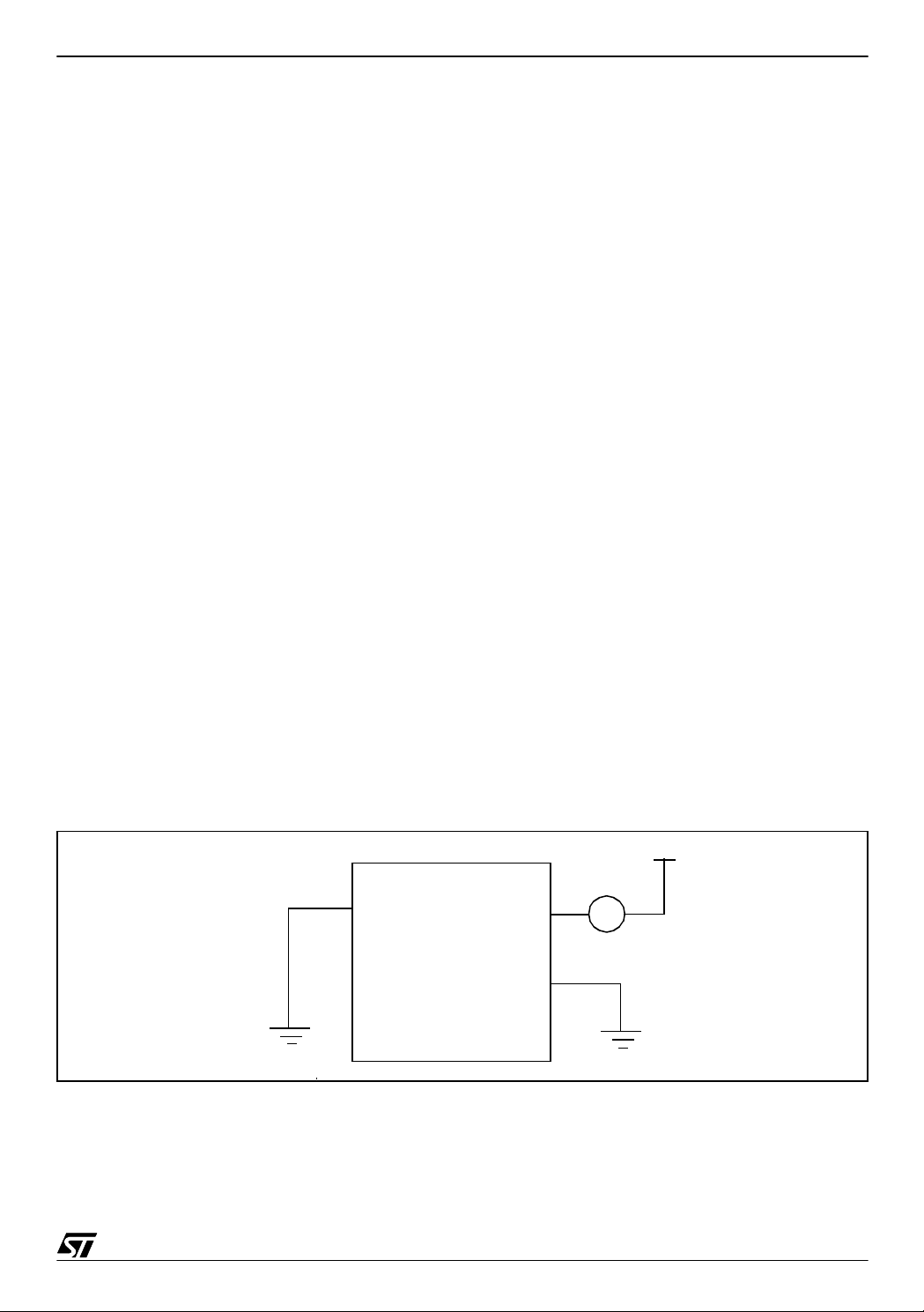
This example provides a static method of measuring the current consumed by the microcontroller in different modes and without any I/O activity. The measurement is done using the following configuration.
6.1.1 Measurement Configuration
– All ports have been set as Push-Pull Outputs at low level.
– All other peripherals are in reset configuration.
– After this, MCU is put into different modes by calling different instructions and by setting
some bits (in the MCCSR register).
– In Option Byte, PLL*2 is disabled, CSS is also disabled and LVD is Off.
Figure 1. Hardware Setup
V
DD
Vpp/ICCSEL
V
DD
mA
ST72324
V
SS
6.1.2 Consumption
The consumption mainly depends on the mode selected and the CPU frequency.
7/25
HOW TO MINIMIZE THE ST7 POWER CONSUMPTION
6.1.2.1 Run Mode Methodology:
A resonator oscillator is used with f
at 4 / 8 MHz. PLL*2 is disabled (So, f
osc
osc2
is f
osc
/2). All
peripherals are in reset configuration except the ports. So, the SMS bit in the MCCSR is reset
to 0. The CP1 and CP0 bits in the MCCSR are also reset to 0 and hence f
CPU
is f
. All ports
osc2
are set as Push-Pull Outputs with low level.
Measurements:
Table 2. Consumption I
f
(MHz) f
OSC
42 3.90 mA 4.38 mA 4.91 mA
84 5.88 mA 6.67 mA 7.42 mA
(MHz) IDD at V
CPU
(RUN Mode) at TA = + 25 °C
DD
= 4.5 V IDD at V
DD
= 5 V IDD at V
DD
DD
= 5.5 V
6.1.2.2 Slow Mode Methodology: A resonator oscillator is used with f
is f
/2. All peripherals are in reset configuration except the ports and the SMS bit in the
osc
at 4 / 8 MHz. PLL*2 is disabled. So, f
osc
osc2
MCCS R is s et to 1. The CP1 a nd CP 0 bi ts in th e MC CSR are set to an ap prop riate value .
Hence f
CPU
is f
osc
/4, f
osc
/8, f
osc
/16, f
/32. Al l po rts a re set as Pus h-P ull Ou tput s w ith low
osc
level.
Measurements:
Table 3. Consumption I
(MHz) f
f
OSC
40.1251.33 mA 1.51 mA 1.70 mA
4 / 8 0.25 1.67 mA 1.93 mA 2.18 mA
4 / 8 0.5 2.25 mA 2.54 mA 2.88 mA
4 / 8 1 2.87 mA 3.25 mA 3.64 mA
823.88 mA 4.46 mA 4.95 mA
(MHz) IDD at V
CPU
(SLOW Mode) at TA = + 25 °C
DD
= 4.5 V IDD at V
DD
= 5 V IDD at V
DD
DD
= 5.5 V
6.1.2.3 Wait Mode Methodology: A resonator oscillator is used with f
is f
/2. All peripherals are in reset configuration except the ports. So, the SMS bit in the
osc
at 4 / 8 MHz. PLL*2 is disabled. So, f
osc
MCCSR is reset to 0. The CP1 and CP0 bits in the MCCSR are also reset to 0 and hence f
is f
8/25
. All ports are set as Push-Pull Outputs with low level.
osc2
osc2
CPU

Measurements:
Table 4. Consumption I
f
(MHz) f
OSC
423.49 mA 3.91 mA 4.39 mA
845.20 mA 5.92 mA 6.62 mA
(MHz) IDD at V
CPU
6.1.2.4 Slow-Wait Mode
HOW TO MINIMIZE THE ST7 POWER CONSUMPTION
(Wai t Mode) at TA = + 25 °C
DD
= 4.5 V IDD at V
DD
= 5 V IDD at V
DD
DD
= 5.5 V
Methodology: A resonator oscillator is used with f
is f
/2. All peripherals are in reset configuration except the ports and the SMS bit in the
osc
at 4 / 8 MHz. PLL*2 is disabled. So, f
osc
osc2
MCCS R is s et to 1. The CP1 a nd CP 0 bi ts in th e MC CSR are set to an ap prop riate value .
Hence f
CPU
is f
osc
/4, f
osc
/8, f
osc
/16, f
/32. Al l po rts a re set as Pus h-P ull Ou tput s w ith low
osc
level.
9/25

HOW TO MINIMIZE THE ST7 POWER CONSUMPTION
Measurements:
Table 5. Consumption I
f
(MHz) f
OSC
40.1251.28 mA 1.44 mA 1.63 mA
4 / 8 0.25 1.59 mA 1.85 mA 2.10 mA
4 / 8 0.5 2.12 mA 2.45 mA 2.77 mA
4 / 8 1 2.69 mA 3.02 mA 3.39 mA
823.56 mA 3.99 mA 4.39 mA
(MHz) IDD at V
CPU
(Slow-Wait Mode) at TA = + 25 °C
DD
= 4.5 V IDD at V
DD
= 5 V IDD at V
DD
6.1.2.5 Active-Halt Mode
DD
= 5.5 V
Methodology: A resonator oscillator is used with f
is f
/2. All peripherals are in reset configuration except the ports. All ports are set as Push-
osc
at 4 / 8 MHz. PLL*2 is disabled. So, f
osc
osc2
Pull Outputs with low level. The MCCSR-OIE bit is set to 1 and the TB1 & TB0 of MCCSR bits
are set to 1. The MCC/RTC interrupt is used as the wake-up interrupt. The oscillator is ON, so
the total consumption also includes the oscillator consumption.
Measurements:
Table 6. Consumption I
f
(MHz) IDD at V
OSC
4 1.06 mA 1.20 mA 1.36 mA
8 1.19 mA 1.35 mA 1.53 mA
(Active-Halt Mode) at TA = + 25 °C
DD
= 4.5 V IDD at V
DD
= 5 V IDD at V
DD
DD
= 5.5 V
6.1.2.6 Halt Mode Methodology: A resonator oscillator is used with F
F
osc2
is F
/2. All peripherals are in reset configuration except the ports. All ports are set as
osc
at 4 / 8 MHz. PL L*2 is dis abled. S o,
osc
Push-Pull Outputs with low level.
Measurements:
Table 7. Consumption I
(MHz) IDD at V
f
OSC
4 0.1 µA0.1 µA0.1 µA
80.1 µA0.1 µA0.1 µA
(Halt Mode) at TA = + 25 °C
DD
= 4.5 V IDD at V
DD
= 5 V IDD at V
DD
DD
= 5.5 V
6.1.3 Conclusion
Current consumption depends on V
f
. In Active-Halt mode, the time base for the MCC/RTC interrupt does not affect the current
OSC
. Consumption increases with the increase of V
DD
DD
and
consumption in this particular application. The osc illator is ON in Active-Halt mode, so the total
consumption also includes the osc illator c onsumpti on. In H alt mod e, c urrent consum p tion is
independent of V
10/25
DD
and f
OSC
.

HOW TO MINIMIZE THE ST7 POWER CONSUMPTION
6.2 EXAMPLE 2: APPLICATION WITH PERIODIC WAKE-UP
This example provides a method for measuring the average current consumed by the micro in
different modes w hile it cycles continuously throug h “wak e-up” and “sleep” periods. The
measurement is done using the following configuration.
6.2.1 Measurement Configuration
- The PF1 port (through which an external i nterrupt is appl ied to MCU) is configured as pull up
interrupt.
- The sensitivity of the interrupt is configured as rising edge.
- Then the capacitor is charged and immediately the MCU is put into the corresponding mode
(Wait, Slow-Wait, Halt) by calling a “WFI” or “HALT” instruction and setting som e bits .
- As soon as the capacitor charges to 0.7V
, the MCU recognizes it as external interrupt and
DD
comes out of low power mode.
- The capacitor is then dis charged by setting the PF1 por t to Push-Pull Output at low level and
a small delay is then provided to let the capacitor discharge fully before charging it the next
time.
- The MCU is again put into the corresponding low power mode and the same process is repeated. The current consumption is measured in continuous interrupted mode.
- In Option Byte, PLL*2 is disabled, CSS is also disabled and LVD is Off.
Figure 2. Hardware Setup
V
DD
V
DD
PF1
ei1
R
PU
V
DD
mA
ST72324
V
C
EXT
Vpp/ICCSEL
SS
6.2.2 Consumption
The cons ump tion ma inly depe nds on how fr equ ently th e MC U wake s up from di fferen t low
power modes. T he W ake- Up t ime i n tur n d epends upon th e RC ti me consta nt. The v alue of
the C
supply of the MCU. R
is fixed but the internal pull up resistance value varies depending upon the power
ext
decreases with the increase of VDD.
PU
11/25

HOW TO MINIMIZE THE ST7 POWER CONSUMPTION
The variation of RPU with temperature and VDD is given in the datasheet.
6.2.2.1 Wait Mode
Methodology: A resonator oscillator is used with f
is f
/2. All peripherals are in reset configuration except the ports. So, the SMS bit in the
osc
MCCSR is reset to 0. The CP1 and CP0 bits in the MCCSR are also reset to 0 and hence F
is f
. IS21 bit of EICR is cleared and IS20 bit of EICR is set to 1. All Ports are in Push-Pull
osc2
at 4 / 8 MHz. PLL*2 is disabled. So, f
osc
osc2
CPU
Output with low level except PF1 (which is used for charging and discharging the capacitor).
Measurements:
Table 8. Consumption I
f
(MHz) f
OSC
423.64 mA 4.06 mA 4.63 mA
845.44 mA 6.16 mA 6.91 mA
(MHz) IDD at V
CPU
(Wait Mode) for C
DD
DD
= 4.5 V IDD at V
= 1 uF at TA = + 25 °C
ext
= 5 V IDD at V
DD
DD
= 5.5 V
6.2.2.2 Slow-Wait Mode
Methodology: A resonator oscillator is used with f
is f
/2. All peripherals are in reset configuration except the ports and the SMS bit in the
osc
MCCSR is set to 1. The CP1 and CP0 bits in the MCCSR are set accordingly. Hence f
f
osc
/4, f
osc
/8, f
osc
/16, f
/32. The IS21 bit in the EICR is cleared and IS20 bi t in the EICR is set
osc
at 4 / 8 MHz. PLL*2 is disabled. So, f
osc
CPU
osc2
is
to 1. All ports ar e set as Push-Pull O utputs with l ow level ex cept PF1 (which is used for
charging and discharging the capacitor).
Measurements:
Table 9. Consumption I
(MHz) f
f
OSC
40.1251.38 mA 1.55 mA 1.78 mA
4 / 8 0.25 1.68 mA 1.93 mA 2.19 mA
4 / 8 0.5 2.24 mA 2.51 mA 2.88 mA
4 / 8 1 2.80 mA 3.17 mA 3.53 mA
823.68 mA 4.16 mA 4.68 mA
(MHz) IDD at V
CPU
(Slow-Wait Mode) for C
DD
= 4.5 V IDD at V
DD
= 1 uF at TA = + 25 °C
ext
= 5 V IDD at V
DD
DD
= 5.5 V
12/25

6.2.2.3 Halt Mode
HOW TO MINIMIZE THE ST7 POWER CONSUMPTION
Methodology: A resonator oscillator is used with f
f
/2. All peripher als ar e in reset config uration ex cept t he p orts. The I S21 bit in th e E ICR i s
osc
at 8 MHz. PLL*2 is disabled. So, f
osc
osc2
is
cleared and the IS20 bit in the EICR is set to 1. All ports are set as Push-Pull Outputs with low
level except PF1 (which is used for charging and discharging the capacitor).
Measurements:
Table 10. Consumption I
f
(MHz) IDD at V
OSC
8 360 µA580 µA 840 µA
(Halt Mode) for C
DD
= 4.5 V IDD at V
DD
= 1 uF at TA = + 25 °C
ext
= 5 V IDD at V
DD
DD
= 5.5 V
6.2.3 Conclusion
increases, RPU decreases. So, the RC time constant also decreases for a fixed value of
If V
DD
C
. So, the wak e-up time de creases. Hence the wak e-up freque ncy incr eases with the in -
ext
crease of V
DD
.
A delay after wake-up by an interrupt exists only in Halt mode, because in all other low power
modes (e xcept Hal t mode ) the osc illator is ON. So, to wake up from HA LT mod e, the MCU
needs 256/4096 CPU cycles delay for the oscillator startup, during this time it consumes some
current.
* Wake-Up frequency is the external interrupt frequency (Wake-Up time is the time after which
the MCU is woken up from the different modes (W ait, Slow -Wai t, Active- Halt, Halt)).
6.3 EXAMPLE 3: APPLICATION WITH PERIODIC WAKEUP AND WATCHDOG
For this exam ple, we as sum e that for th e ap plica tion th e W atchdog Time r (WDG) has to remain active and that the mic rocontroller has to stay in low power mode for an undefined time
period. Therefore, Halt mod e c an not b e used, as the “Halt” instruction rese ts the micr ocontroller when the WDG is active and WDGHALT option bit in the option byte is set to 1. When
the WDGHALT option bit in the option byte is 0 and WDG is active, a “ Halt” instruction doesn’t
generate a Watchdog reset. In this case, the MCU enters Halt mode. The Watchdog counter
is decremented once and then stops c ounting and is no longer able to gene rate a watchdog
reset until the MCU receives an external interrupt or r eset.
Active-Halt mode can also not be
used, because, the device cannot spend more than a defined period in this power saving
mode. Consequ ently, Wait mode is u sed, ass ociated wi th Slow mo de configur ed for the
slowest frequency. This slow mode clock (f
) drives the active peripherals and the CPU
CPU
when it is woken-up. Of course, to reduce power consumption fur ther, Halt mode should be
used wherever possible.
In terms of applications, users usually try to optimize the power consumption during the wait
loop in the main program. In this configuration the microcontroller is mostly idle, waiting for an
13/25

HOW TO MINIMIZE THE ST7 POWER CONSUMPTION
external event, or regularly woken-up by an internal ti mer event. In our case, w e decided to put
the ST7 core in Wait For Interrupt state, with one timer active to regularly wake up the core.
This enables the core to refresh the WDG to prevent a watchdog reset. The clock driving the
active peripherals and the core when it is active corresponds to the slowest clock available. It
is the oscillator clock divided by 2 then divided by 16. So the clock driving the peripherals and
core (f
) is equal to the crystal value (f
CPU
) divided by 32. The measurement is done using
OSC
the following configuration.
6.3.1 Measurement Configuration
In this mode, the MCU is configured as below, but of course in the application this configuration may differ, in particular the I/O port used.
- The optimum Slow mode is selected with the divided external clock factor equal to 32. This
clock (f
) drives the active peripherals (WDG and Timer A) and the core when it is active. In
CPU
the Miscellaneous Register (MISCR) the SMS and CP1 & CP 0 bits must be set.
- All I/O ports ar e connected to an external pul l-up or pul l-down to avoid leak age due to floating
inputs.
- The Watchdog Timer ( WDG) is active with a maximum time- out period. T he WDG Cont rol
Register (WDGCR) must be loaded with the value FFh and the TB1 & T B0 bits m ust be s et.
- One 16-bit timer is used to wake-up the core at regular intervals. The timer event period must
be adjusted to its maximum value to allow the core to refresh the WDG and to a void a WDG
reset. The timer clock equals f
/8, in the Control Register (CR2), CC1 bit must be set & CC0
CPU
bits must be cleared.
- The external clock is selected on the unused 16-bit timer with a continuous level on the external clock pin. In the Control Register (CR2) CC1, CC0 bits mus t be set.
Note: If timer A is used to regularly wake-up the WDG, the user only has to select the external
clock on timer B. The continuous level on the timer input clock is already done internally, as
there is no external I/O connected to the internal Timer B circuit. It stops the counter on timer
B, because if external clock is not available, programming the external clock configuration
stops the counter.
On the contrary, if Timer B is use d to w ake-up the m icro, the user has to select the ext ernal
clock on Timer A and to fix a continuous level on the external clock pin. But be aware, on
Timer A there is only one input capture and one output compare instead of two on Timer B.
– The main loop contains a Wait For Interrupt “WFI” instruction.
– Continuous low level on each PWM output (reset state)
– The A/D converter must be switched off. In the A/D Control/Status Register (CSR), the
ADON bit must be cleared.
– The SPI and SCI are unused.
14/25

HOW TO MINIMIZE THE ST7 POWER CONSUMPTION
– In Option Byte, PLL*2 is disabled, CSS is also disabled and LVD is Off.
For the ST7 software configuration, please refer to your datasheet.
Figure 3. Hardware Setup
V
DD
R
DOWN
Port A, Port B ,
Port C, Port D,
Port E & Port F
V
DD
mA
ST72324
Vpp/ICCSEL
V
SS
6.3.2 Application Methodology: A resonator oscillator is used with f
is f
/2. All peripherals are in reset configuration and the SMS bit in the MCCSR is set to 1.
osc
The CP1 and CP0 bits in the MCCSR are s et to 1. Hence f
at 4 / 8 MHz. PLL*2 is disabled. So, f
osc
CPU
is f
/32. The TB1 and TB0 bits
osc
osc2
in the MCCSR are set to 1. All I/O ports are c onnected to an exter nal pull-down. OC IE bit of
TACR1 is set to 1. CC1 bit of TACR2 is set to 1 and CC0 bit of TACR2 is cleared. CC1 and
CC0 bits of TBCR2 are set to 1.
Measurements:
The me asure me nt of cu rr ent ( I
) is done directly on the VDD pin. The mic rocon troller is in
DD
Wait mode and is configured as described above, with the WDG and one 16-bit Timer active.
The values given in Table11 correspond to typical measured values. They are not maximum
or minimum values.
Table 11. Consumption I
f
(MHz) f
OSC
4 125 1.26 mA 1.43 mA 1.62 mA
8 250 1.54 mA 1.80 mA 2.02 mA
(kHz) IDD at V
CPU
at TA = + 25 °C
DD
= 4.5 V IDD at V
DD
= 5 V IDD at V
DD
DD
= 5.5 V
6.3.3 Conclusion
Current con sum ptio n depe nds on V
V
DD
and F
. In this particular application, Timer B i s disabled. So, by disabli ng the Timer B,
OSC
. Current cons umpti on increas es with the inc rease of
DD
current consumption reduces . CPU frequency and Tim er frequenc y also dec ides the current
consumption.
15/25

HOW TO MINIMIZE THE ST7 POWER CONSUMPTION
7 APPENDI X B: ST7FLITE0 STANDARD EXAMPLES
This section provides examples of how to minimise the consumption in a particular ST7 application for device ST7FLITE09.( Use ST7LITE0 datasheet for a reference)
7.1 EXAMPLE 1: STATIC MEASUREMENT
This example provides a static method of measuring the current consumed by the microcontroller in different modes and without any I/O activity. The measurement is done using the following configuration.
7.1.1 Measurement Configuration
– All ports have been set as Push-Pull Outputs at low level.
– All other peripherals are in reset configuration.
– After this, MCU is put into different modes by calling different instructions and by setting
some bits (in the MCCSR & ATCSR r egisters).
– In Option Byte, PLL is disabled, Internal RC Oscillator is OFF, LVD is OFF & No Reset when
Halt is selected.
Figure 4. Hardware Setup
V
DD
V
DD
mA
ST7LITE0
V
SS
7.1.2 Consumption
The consumption mainly depends on the mode selected, CPU frequency & Supply voltage.
16/25

HOW TO MINIMIZE THE ST7 POWER CONSUMPTION
7.1.2.1 Run Mode Methodology: An external CLK source, up to 16M Hz is used on pin CLKIN. PL L is disabled
and internal RC Oscillator is OFF. So, f
tion except the I/O Ports. At reset the SMS bit in the MCCSR is 0, hence f
is CLKIN / 2. All peripherals are in reset configura-
OSC
is f
CPU
OSC
. All Ports
are in Push-Pull Outputs with low level.
Measurements:
Table 12. Consumption I
External CLK
on CLKIN Pin
(MHz)
16 8 4.5 mA 5.17 mA 5.86 mA
84 2.32 mA 2.68 mA 3.07 mA
f
(MHz) IDD at V
CPU
(RUN Mode) at TA = + 25 °C
DD
= 4.5 V IDD at V
DD
= 5 V IDD at V
DD
DD
= 5.5 V
7.1.2.2 Slow Mode Methodology: An external CLK source, up to 16M Hz is used on pin CLKIN. PL L is disabled
and internal RC Oscillator is OFF. So, f
tion except the I/O Ports and the SMS bit in the MCCSR is set to 1, hence f
is CLKIN / 2. All peripherals are in reset configura-
OSC
is f
CPU
OSC
/32. All
Ports are in Push-Pull Outputs with low level.
Measurements:
Table 13. Consumption I
External CLK
on CLKIN Pin
(MHz)
16 0.25 417 µA490 µA 571 µA
80.125 274 µA320 µA 372 µA
2 0.03125 142 µA161 µA 192 µA
f
(MHz) IDD at V
CPU
(SLOW Mode) at TA = + 25 °C
DD
= 4.5 V IDD at V
DD
= 5 V IDD at V
DD
DD
= 5.5 V
17/25

HOW TO MINIMIZE THE ST7 POWER CONSUMPTION
7.1.2.3 Wait Mode Methodology: An external CLK source, up to 16M Hz is used on pin CLKIN. PL L is disabled
and internal RC Oscillator is OFF. So, f
tion except the I/O Ports. At reset the SMS bit in the MCCSR is 0, hence f
is CLKIN / 2. All peripherals are in reset configura-
OSC
is f
CPU
OSC
. All Ports
are in Push-Pull Outputs with low level.
Measurements:
Table 14. Consumption I
External CLK
on CLKIN Pin
(MHz)
16 8 1434 µA 1685 µA 1920 µA
84 907 µA 1054 µA 1205 µA
21 315 µA365 µA 433 µA
f
(MHz) IDD at V
CPU
(Wai t Mode) at TA = + 25 °C
DD
= 4.5 V IDD at V
DD
= 5 V IDD at V
DD
DD
= 5.5 V
7.1.2.4 Slow-Wait Mode Methodology: An external CLK s ource, up to 16M Hz is used on pin CL KIN. PLL is disabled
and internal RC Oscillator is OFF. So, f
tion except Ports and the SMS bit in the MCC SR is set to 1, hence f
is CLKIN / 2. All peripherals are in reset configura-
OSC
CPU
is f
/32. All Ports
OSC
are in Push-Pull Outputs with low level.
Measurements:
Table 15. Consumption I
External CLK
on CLKIN Pin
(MHz)
16 0.25 337 µA402 µA 475 µA
80.125 230 µA270 µA 316 µA
2 0.03125 128 µA146 µA 170 µA
f
(MHz) IDD at V
CPU
(Slow-Wait Mode) at TA = + 25 °C
DD
= 4.5 V IDD at V
DD
= 5 V IDD at V
DD
DD
= 5.5 V
18/25

HOW TO MINIMIZE THE ST7 POWER CONSUMPTION
7.1.2.5 Active-Halt Mode Methodology: An external CLK source, up to 16M Hz is used on pin CLKIN. PL L is disabled
and internal RC Oscillator is OFF. So, f
is CLKIN / 2. All peripherals are in reset configura-
OSC
tion except the I/O Ports. All P orts are in Push- Pull Outputs w ith low l evel. Set A TCSR- CK1
bit to 0 & CK0 & OVFIE bits to 1. MCU is woken-up by AT TIMER Overflow Interrupt. The oscillator is ON, so the total consumption includes the oscillator consumption also.
Measurements:
Table 16. Consumption I
External CLK
on CLKIN Pin
(MHz)
16 8 366 µA428 µA 501 µA
84 238 µA277 µA 321 µA
21 122 µA136 µA 157 µA
(MHz) IDD at V
f
CPU
(Active-Halt Mode) at TA = + 25 °C
DD
= 4.5 V IDD at V
DD
= 5 V IDD at V
DD
DD
= 5.5 V
7.1.2.6 Halt Mode Methodology: An external CLK source, up to 16MH z is used on pin CLKIN. PL L is disabled
and internal RC Oscillator is OFF. So, f
is CLKIN / 2. All peripherals are in reset configura-
OSC
tion except Ports. All Ports are in Push-Pull Outputs with low level.
Measurements:
Table 17. Consumption I
External CLK
on CLKIN Pin
(MHz)
16 8 0.1 µA0.1 µA0.1 µA
84 0.1 µA0.1 µA0.1 µA
f
(MHz) IDD at V
CPU
(Halt Mode) at TA = + 25 °C
DD
= 4.5 V IDD at V
DD
= 5 V IDD at V
DD
DD
= 5.5 V
7.1.3 Conclusion
Current consumption depends on V
. Consumption increas es with the increase of VDD and
DD
External clock frequency. The o scillator i s ON i n Active- Halt m ode, so the total c onsumption
includes the oscillator consumption also. In Halt mode, current consumption is independent of
V
and External clock frequency.
DD
7.2 EXAMPLE 2: APPLICATION WITH PERIODIC WAKE-UP
This example provides a method for measuring the average current consumed by the micro in
different modes w hile it cycles continuously throug h “wak e-up” and “sleep” periods. The
measurement is done using the following configuration.
19/25

HOW TO MINIMIZE THE ST7 POWER CONSUMPTION
7.2.1 Measurement Configuration
– The port PA0 (through which external interrupt is applied to MCU) is configured as pull up
interrupt.
– The sensitivity of the interrupt is configured as rising edge.
– Then the capacitor is charged and immediately the MCU is put into the corresponding mode
(Wait, Slow-Wait, Halt) by calling “WFI” or “HALT” instruction and setting some bits.
– As soon as the capacitor charges to 0.7Vdd, the MCU takes it as external interrupt and
comes out of that mode.
– The capacitor is then discharged by setting PA0 port to Push-Pull Output at low level and
small delay is then provided to let the capacitor discharge fully before charging it next time.
– The MCU is again put into corresponding mode and the same process is repeated. The
Measurement of current consumption is done in continuous interrupted mode.
– In Option Byte, PLL is disabled, Internal RC Oscillator is OFF, LVD is Off & No Reset when
Halt is selected.
Figure 5. Hardware Setup
V
DD
V
DD
C
EXT
PA0
ei0
R
PU
ST7LITE0
V
DD
V
SS
mA
7.2.2 Consumption
The consumption main ly depends on the Wake-Up frequ ency of the MCU from differ ent
modes. The Wake-Up time in turn depends upon the RC time constant. The value of the C
EXT
is fixed but the internal pull up resistance value varies depending upon the voltage supply of
the MCU. R
The variation of R
decreases with the increase of VDD.
PU
with VDD is given in the datasheet.
PU
7.2.2.1 Wait Mode Methodology: An external CLK source, up to 16M Hz is used on pin CLKIN. PL L is disabled
and internal RC Oscillator is OFF. So, f
tion except Ports. At reset the SMS bi t is 0, hence f
20/25
is CLKIN / 2. All peripherals are in reset configura-
OSC
CPU
is f
. The IS01 bit in the EICR reg-
OSC

HOW TO MINIMIZE THE ST7 POWER CONSUMPTION
ister is cleared and the IS00 bit in the EICR register is set to 1. All Ports are in Push-Pull
Output with low level except PA0 (which is used for charging and discharging the capacitor).
Measurements:
Table 18. Consumption I
External CLK
on CLKIN Pin
(MHz)
16 8 1850 µA 2087uA 2380uA
84 1195uA 1426uA 1590uA
f
(MHz) IDD at V
CPU
(Wait Mode) for C
DD
= 4.5 V IDD at V
DD
= 1 uF at TA = + 25 °C
EXT
= 5 V IDD at V
DD
DD
= 5.5 V
7.2.2.2 Slow-Wait Mode Methodology: An external CLK source, up to 16M Hz is used on pin CLKIN. PL L is disabled
and internal RC Oscillator is OFF. So, f
tion except the I/O Ports and the SMS bit of in the MCCSR register is set to 1, hence f
f
/32.The IS01 bit in the EICR register is cleared and the IS00 bit in the EICR register is set
OSC
is CLKIN / 2. All peripherals are in reset configura-
OSC
CPU
is
to 1. All Ports are in Push-Pull Outputs with low level except PA0 (which is used for charging
and discharging the capacitor).
Measurements:
Table 19. Consumption I
External CLK
on CLKIN Pin
(MHz)
16 0.25 430uA 526uA 612uA
80.125 293uA 380uA 434uA
4 0.0625 220uA 280uA 333uA
f
(MHz) IDD at V
CPU
(Slow-Wait Mode) for C
DD
= 4.5 V IDD at V
DD
= 1 uF at TA = + 25 °C
EXT
= 5 V IDD at V
DD
DD
= 5.5 V
7.2.2.3 Halt Mode Methodology: An external CLK source, up to 16MH z is used on pin CLKIN. PL L is disabled
and internal RC Oscillator is OFF. So, f
is CLKIN / 2. All peripherals are in reset configura-
OSC
tion except Ports. IS01 bit of EICR is cleared and IS00 bit of EICR is set to 1. All Ports are in
Push-Pull Outputs with low level except PA0 (which is used for charging and discharging the
capacitor).
Measurements:
Table 20. Consumption I
f
(MHz) IDD at V
CPU
8 95 µA115 µA 143 µA
(Halt Mode) for C
DD
= 4.5 V IDD at V
DD
= 1 uF at TA = + 25 °C
EXT
= 5 V IDD at V
DD
DD
= 5.5 V
21/25

HOW TO MINIMIZE THE ST7 POWER CONSUMPTION
7.2.3 Conclusion
increases, RPU decreases. So, the RC time constant also decreases for a fixed value of
If V
DD
C
. So, the wake-up time decreases. Hence wake-up frequency increases with the increase
EXT
DD
.
of V
Temporizat ion peri od exis ts onl y i n Halt mo de in c a se o f I nte rrupt , becau se d uring al l ot her
modes (except Halt mode) oscillator is ON. So, in HALT mode, the MCU needs 256 CPU cycles as temporization period, during that time it consumes some current.
* Wake-Up frequency is the external interrupt frequency (Wake-Up time is the time after which
the MCU is woken up from the different modes (Wait, Slow-Wait, Halt)).
7.3 EXAMPLE 3: APPLICATION WITH PERIODIC WAKEUP AND WATCHDOG
For this exam ple, we as sum e that for th e ap plica tion th e W atchdog Time r (WDG) has to remain active and that the mic rocontroller has to stay in low power mode for an undefined time
period. Therefore, Halt mod e c an not b e used, as the “Halt” instruction rese ts the micr ocontroller when the WDG is active and WDGHALT option bit in the option byte is set to 1. When
the WDGHALT option bit in the option byte is 0 and WDG is active, a “ Halt” instruction doesn’t
generate a Watchdog reset. In this case, the MCU enters Halt mode. The Watchdog counter
is decremented once and then stops c ounting and is no longer able to gene rate a watchdog
reset until the MCU receives an external interrupt or r eset.
Active-Halt mode can also not be
used, because, the device cannot spend more than a defined period in this power saving
mode. Consequ ently, Wait mode is u sed, ass ociated wi th Slow mo de configur ed for the
slowest frequency. This slow mode clock (f
) drives the active peripherals and the CPU
CPU
when it is woken-up. Of course, to reduce power consumption fur ther, Halt mode should be
used wherever possible.
In terms of applications, users usually try to optimize the power consumption during the wait
loop in the main program. In this configuration the microcontroller is mostly idle, waiting for an
external event, or regularly woken-up by an internal ti mer event. In our case, w e decided to put
the ST7 core in Wait For Interrupt state, with one timer active to regularly wake up the core.
This enables the core to refresh the WDG to prevent a watchdog reset. The clock driving the
active peripherals and the core when it is active corresponds to the slowest clock available. It
is the oscillator clock divided by 2 then divided by 32. So the clock driving the peripherals and
core (f
) is equal to the f
CPU
/32. The m easuremen t is d one usin g the fol lowing confi gura-
OSC
tion.
7.3.1 Measurement Configuration
In this mode, the MCU is configured as below, but of course in the application this configuration may differ, in particular the I/O port used.
22/25

HOW TO MINIMIZE THE ST7 POWER CONSUMPTION
– Slow mode is selected with the divided external clock factor equal to 64. This clock (f
CPU
)
drives the active peripherals (WDG and LT-Realtime Clock) and the core when it is active.
In the Main Clock Control/Status Register (MCCSR) the SMS bit must be set.
– All I/O ports are connected to an external pull-up or pull-down to avoid leakage due to floating
inputs.
– The Watchdog Timer (WDG) is active with a 2msec time-out period.
– Here 8 bit LT is used to wake-up the core at regular intervals, 1msec, to avoid a WDG reset.
– In LTCSR register set, TB to 0 & TBIE to 1.
– The main loop contains a Wait For Interrupt “WFI” instruction.
– Here all other peripherals (except above) are OFF
– Set Option Byte “value” to “FC FE” (In Option Byte, PLL = disabled, RC Oscillator = OFF,
LVD = OFF, WDG SW = Software, WDG HALT= No Reset when Halt)
– For the ST7 software configuration, please refer to your datasheet.
Figure 6. Hardware Setup
V
DD
R
DOWN
Port A, Port B
V
DD
mA
ST7LITE0
V
SS
7.3.2 Application Methodology: An external CLK source, up to 16MHz is used on pin CLKIN. PLL is disabled
and internal RC Oscillator is OFF. So, f
tion and the SMS bit in the MCCSR is set to 1.H ence f
is CLKIN / 2. All peripherals are in reset configura-
OSC
CPU
is f
/32. All I/O ports are con-
OSC
nected to an external pull-down.
Measurements:
The measurement of current (I
) is done directly on the VDD pin. The microcontroller is in
DD
Wait mode and is configured as described above, with the WDG and LT Timer active.
The values given in Table21 correspond to typical measured values. They are not maximum
or minimum values.
23/25

HOW TO MINIMIZE THE ST7 POWER CONSUMPTION
Table 21. Consumption IDD at TA = + 25 °C
External CLK
on CLKIN Pin
f
(MHz) IDD at V
CPU
= 4.5 V IDD at V
DD
= 5 V IDD at V
DD
(MHz)
16 0.25 369 µA425 µA 500 µA
80.125 250 µA283 µA 338 µA
2 0.03125 149 µA187 µA 245 µA
7.3.3 Conclusion
DD
= 5.5 V
Current consumption depends on V
V
and F
DD
OSC
.
. Current consumption increases with the increase of
DD
24/25

HOW TO MINIMIZE THE ST7 POWER CONSUMPTION
THE PRESENT NOTE WHICH IS FOR GUIDANCE ONLY AIMS AT PROVIDING CUSTOMERS WITH INFORMATION
REGARDING THE IR PRO DUCT S IN OR DER FO R THEM TO SAV E TIME . AS A RES ULT, STMIC ROEL ECTR ONI CS
SHALL NOT BE HELD LIABLE FOR ANY DIRECT, INDIRECT OR CONSEQUENTIAL DAMAGES WITH RESPECT TO
ANY CL AIM S AR IS IN G FR OM T HE CO N TENT OF S UC H A NO TE A ND /O R T HE U SE M AD E BY C US TO ME RS O F
THE INFORMATION CONTAINED HEREIN IN CONNECTION WITH THEIR PRODUCTS.”
Information furnished is believed to be accurate and reliable. However, STMicroelectronics assumes no responsibility for the consequences
of use of such information nor for any infringement of patents or other rights of third parties which may result from its use. No license is granted
by implic ation or otherwise under any patent or patent ri ghts of STM i croelectr oni cs. Spec i fications mentioned i n this publication are subje ct
to change without notice. This publication supersedes and replaces all information previously supplied. STMicroelectronics products are not
authorized for use as cri tical comp onents in life support dev i ces or systems wi thout the express written approv al of STMicroel ectronics.
The ST logo is a registered trademark of STMicroelectronics
2003 STMicroelectronics - All Rights Reserved.
STMicroelectronics Group of Compan i es
http://www.s t. com
Purchase of I
2
C Components by STMicroelectronics conveys a license under the Philips I2C Patent. Rights to use the se components in an
2
I
C system i s granted pro vi ded that the sy stem conforms to the I2C Standard Specification as defined by Philips.
Australi a - B razil - Canada - China - Finl and - France - Germany - Hong Kong - Ind ia - Israel - Italy - Japan
Malaysi a - M al ta - Morocco - Singapore - Spain - Sw eden - Switz erland - United Kingdom - U.S.A.
25/25
 Loading...