AN1009
APPLICATION NOTE
“Negative Undershoot” NVRAM Data Corruption
Miniaturisation in microelectronics has led, inevitably, to the inadvertent appearance of parasitic devices.
Adjacent conducting paths end up being separated by a gap that is so narrow that it ceases to isolate them
properly from each ot her. Parasitic tunnelling devices, bipolar t ransistors, and thyristors end up be ing
formed, with each one causing its own distinctive misbehaviour.
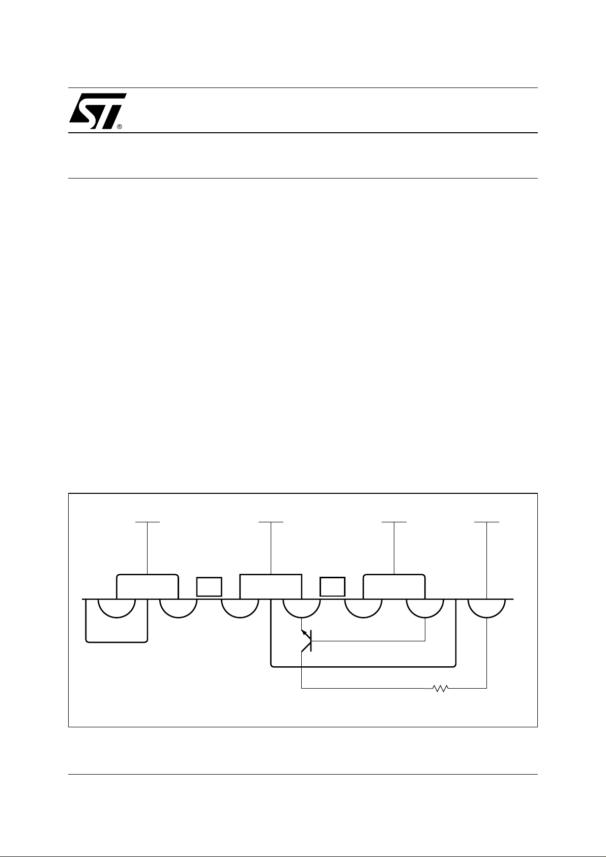
The occurrence of parasitic SCRs (silicon controlled rectifiers) causes the well-studied problem of latchup. The occurrence of parasitic bipolar transistors, such as t he one shown in Figure 1, is normally less
serious, but leads to a particular type o f problem in battery-powe red circuits . It is this probl em th at is addressed in this document.
The problem manifests itself in battery-powered memory as data corruption: the unintentional flipping from
1 to 0, or from 0 to 1, of bits of data in the memory array. It is caused when a negative pulse is inadvertently
applied to the emitter of an inadvertently formed parasitic bipolar transistor, causing it to go into conduction
mode, and to connect two otherwise isolated signal lines.
ANATOMY OF A PARASITIC BIPOLAR TRANSISTOR
Figure 1 shows the cross sec tion o f a CM OS gate, with one MOS FET formed directly in the N-type substrate, and the other in a P-well. Under certain cond itions, the P-wel l can s tart to beh ave as the bas e region of a parasitic bipolar NPN transistor, with the N-type sub strate as its collector region, and the N+
diffusion contact of the MOSFET as its emitter region.
Figure 1. Cross-Section of an NPN Parasitic Bipolar Transistor
GROUNDED
P-WELL
N-SUBSTRATE
VCC
GATE
PAD
(NEGATIVE PULSE)
P+ N+P+N+
VSS
GATE
P+N+
GROUNDED P-WELL
INTERNAL POWER
SUBSTRATE
VCC
N+
AI02522
December 1998 1/4

AN1009 - APPLICATION NOTE
The P-well is held at groun d, so t he p aras itic NPN t ransistor should nev er turn on. If, though, a negative
pulse is applied to the pad, a nd hence to the emitter of t he p aras itic NPN t ransisto r, the transistor wo uld
be put into its conducting mode. Once the pad is taken to -V
and pulls current from the substrate.
When the memory device is being powered by the external power source, the effect of this extra parasitic
current will be neglig ible, and will b e com pensated fo r by the ex ternal power sour ce. Whe n the me mory
device is being powered from the internal battery, though, the battery is unable to compensate for the extra
current, and so the supply voltage will fall. As soon as the supply voltage falls below a crit ical value, SRAM
cells in the memory array will cease to hold their stored data reliably.
The parasitic bipolar transistor starts to turn on when the pad is taken to about -0.6 V. In battery mode, the
impact on the substrate will start to be felt once the current drain through the bipolar transistor is approximately -0.6 mA. The substrat e will be pulled to approximately 1.0 V once the current through the bipolar
transistor reaches -1.5 mA. As the magnitude of the negative current increases, it directly reduces the level of internal V
(the substrate voltage). A current drain of approximately -2.0 mA will bring internal V
CC
to ground, thus leaving the SRAM array completely unpowered.
, the parasitic bipolar transistor turns on,
be
CC
Figure 2. Substrate V
versus Negative Undershoots
CC
AI02521
4V
Substrate V
not
trig'd
M
C1
-1V
-420ns 3.85µs
Negative Undershoot
CC
-1.2 volts for 100ns
-1.2 volts for 500ns
-1.2 volts for 1µs
400ns
500mV
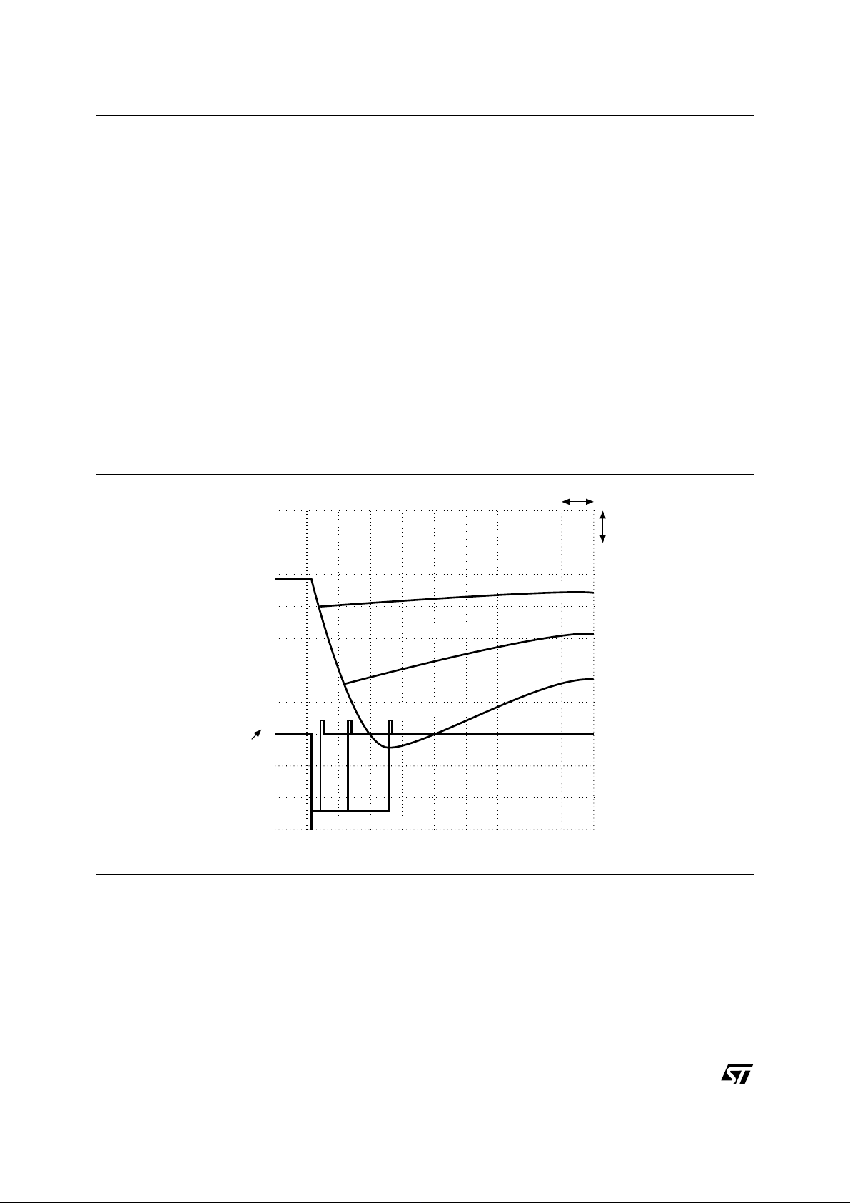
Figure 2 superimposes three pa irs of curves : three negat ive und ersh oot pulses of 100, 500 and 1000 ns
duration; and the corresponding effects that are felt by the V
substrate voltage.
CC
Thus, we see that the effect on the substrate voltage is proportional to the duration of the negative undershoot pulse. It is also proportional to its magnitude (its amplitude). It is also proportional to the number of
pins that receive the negative undershoot pulse (t he example, above, is the effect of just one pin on the
chip going negative).
2/4

AN1009 - APPLICATION NOTE
REMEDIES
ST is continually making design and process modifications to improve the performance of its products.
Immunity to negative undershoot will be improved over time, but only where it does not have a negative
impact on other performance measures, such as operating speed.
The application designer is, therefore, advised to take steps to avoid negative undershoot pulse from being introduced. The first step is to improve the cleanliness of eac h of the signal s. Table 1 lists the pins of
ST’s NVRAMS that are affected (those that consist of an N+ diffusion in a P-well on an N-type substrate).
Table 1. List of the Pins on Devices that are Affected by the Problem
Device Substrate Type PIns Connected to N+ Diffusion
M40Z111 N- 13, 16
M40Z300 N- 4, 10, 13, 16, 20, 22, 23
M48Z02, M48Z12 N- All
M48Z08, M48Z18 P- none (not applicable)
M48Z58, M48Z59 N- 1, 11-13, 19-15, 26, 28
M48Z35 N- All
M48T02, M48T12 N- All
M48T08, M48T18 P- none (not applicable)
M48T58, M48T59, M48T559 N- 1, 11-13, 15-19, 26, 28
M48T35 N- All
M48T37 N- 1, 4-10, 13, 15-20, 22-26, 30,31,33-39
All pins that are c onnected to N+ diffusion are s usceptible t o negat ive undershoot , but spec ial attent ion
should be given to the V
pin. This is connected to internal circuitry that increases the pin’s sensitivity to
CC
negative undershoots, to the extent that pulses of greater than -0.3 V may affect the substrate voltage.
The second step, therefore, is to clamp the power lines (V
and VSS) with a Schottky diode, to short out
CC
any attempt by them to g o negative. Its effectivenes s depends on its speed of operation set agai nst the
speed and energy content of the negative-going pulse (the current sink capability of the pulse). An off-theshelf diode with a V
of approximately 0.32 V, and a current rating of 100 mA, will generally reduce the
be
occurrence of the problem to negligible proportions. However, the higher the current sink capability of the
negative pulse, the more likely an RF Schottky diode is required.
The Schottky diode should be placed as close to the device pin as possible.
V
can be subject to mechani cal noise, the switchin g of VCC on and off, and to negative spikes c om ing
CC
from the power supply during initial power up. The third step, then, is to clean up the power supply, particularly its behaviour at power-on and power-off, where the memory device is expected to continue to
power itself from its internal battery. Particular care should be taken when working with programmable
power supplies. Forcing a programmable power s upply from a positive voltage to 0 volts without taking
care to step down the voltage can generate a negative undershoot pulse.
The fourth step is to protect each of the pins, mentioned in Tabl e 1, by its ow n individual Sc hot tky diode.
No pin should exceed -0.3 V, and their collective reverse current should not be allowed to exceed -1.0 mA,
especially when the memory device is being battery-powered.
3/4

AN1009 - APPLICATION NOTE
If you have any questions or suggestions concerning the matters raised in this document, please send
them to the following electronic mail addresses:
apps.nvram@st.com
ask.memory@st.com
Please remember to include your name, company, location, telephone num ber and fax number.
(for application support)
(for general enquiries)
Information furnished is believed to be accurate and reliable. However, STMicroelectronics assumes no responsibility for the consequences
of use of such information nor for any infringement of patents or other rights of third parties which may result from its use. No license is granted
by implic ation or oth erwise under any patent or pat ent rights of STMicroelectronic s. Specifications mentioned in this publication are subject
to change without notice. This publication supersedes and replaces all information previously supplied. STMicroelectronics products are not
authorized for use as critical comp onents in life support devi ces or systems wi thout express written approval of STM i croelectronics.
© 1998 STMicroelectronics - All Rights Reserved
The ST logo is a registered trademark of STMicroelectronics.
All other na m es are the prop erty of their res pective owners.
STMicroelectronics GROUP OF COMPANIES
Australia - Brazil - China - France - Germany - Italy - Japan - Korea - Malaysia - Malta - Mexico - Morocco - The Netherlands - S i ngapore -
Spain - Sweden - Switze rl and - Taiwan - Th ai land - United Kingdom - U.S.A.
http://www.s t. com
4/4
 Loading...