

Page 1
AN1007
®
APPLICATION NOTE
L6561 - BASED SWITCHER REPLACES MAG AMPS IN
SILVER BOXES
by Claudio Adragna
Mag amps (a contraction of "Magnetic Amplifier") are widely used in multi-output switching power
supplies to get auxiliary regulated power rails. However, they are expensive, bulky, and require a
high level of design expertise.
ST’s L6561, an 8-pin Transition Mode PFC (Power Factor Corrector) controller, is surprisingly suitable for implementing a switch-mode architecture as an alternative to mag amps. Much better performance, a dramatic reduction of part s count, cost and design effort are the benefit s of such an approach. Drawbacks? None. And once more the L6561 turns out to be a really versatile device.
Introduction
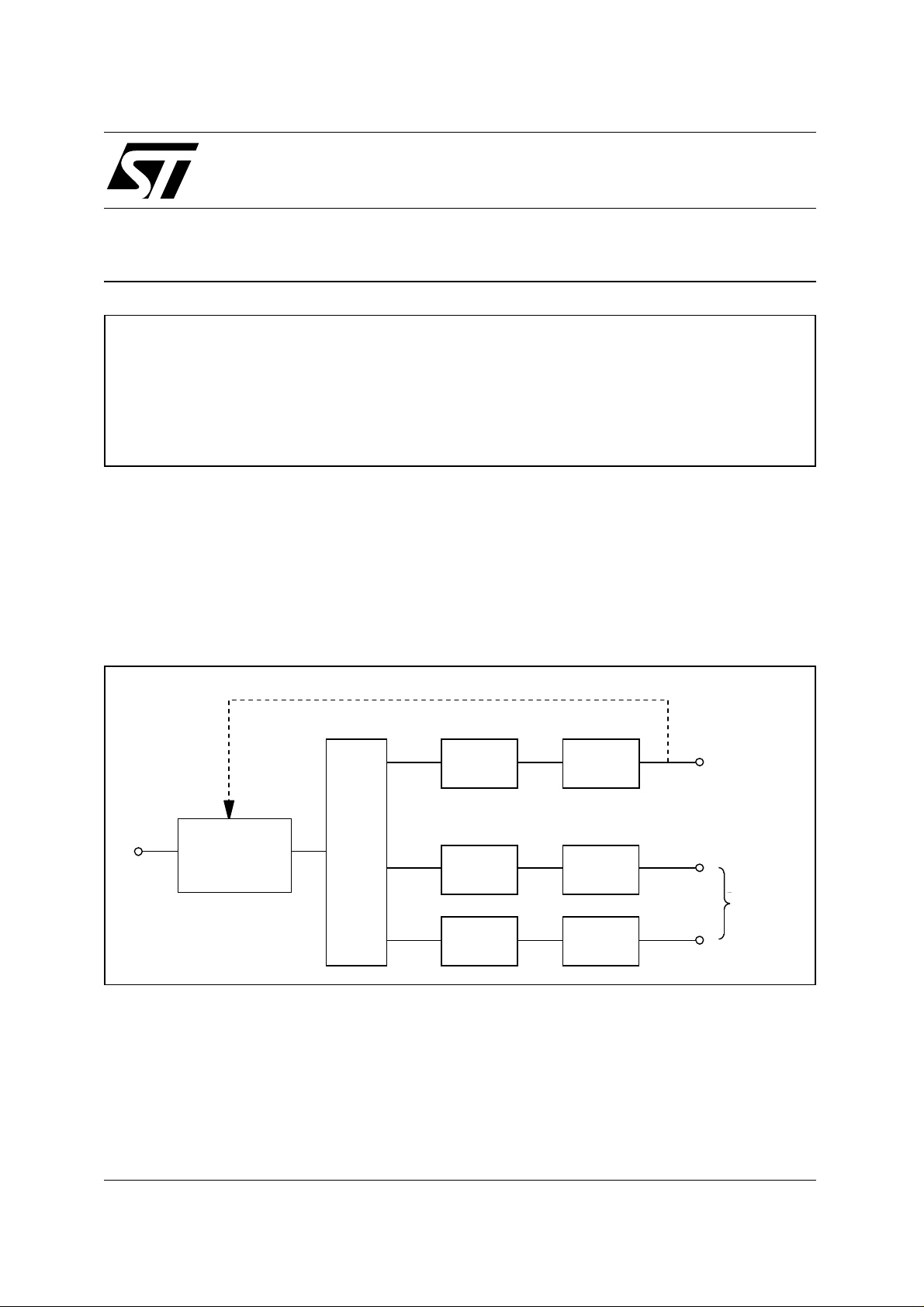
Desktop computer power supplies provide two or more low-voltage, high-current, isolated power rails,
typically a 5V rail and a 12V r ail. More an more of ten, it also provides a 3.3V auxiliary rail with high-current capability.
The power is generated by an off -line forward switching c onverter (inside the s o-called "silver box") that
regulates only one power rail t hrough an isolated feedback loop. The other power rails are usually postregulated to meet the specifications on the output voltage tolerance and regulation. A typical architecture
is shown in fig. 1.
Figure 1. Typical architecture of an SMPS for desktop computer ("silver box").
(ISOLATED) FEEDBACK
MAIN
OUTPUT
AUXILIARY
DC OUTPUTS
DC Input
PWM CONTROLLER
& POWER SWITCH
RECTIFIER
MAG AMP
REGULATOR
MAIN TRANSFORMER
RECTIFIER
+
FIL TER
FIL TER
RECTIFIER
+
FIL TER
LINEAR
REGULATOR
Many power supply manufacturers us e m agnetic am plifiers (in short, "mag amps") to achiev e s econdary
post-regulation. Mag amps regulate the output voltage with a saturable core reactor that exhibits a
square B-H loop: when not saturated, the core material has a very high permeability and the reactor a
very high impedance, then it abruptly saturates thus the permeability drops to a very low value and so
does the impedance of the reactor.
By varying the magnetic DC flux inside the core, mag amps control the time needed for the core to saturate under a given input voltage pulse. Therefore, the reactor acts basically as a delayed switch and perform PWM by modulating the leading-edge of the input voltage pulse applied to the output section.
October 2003
1/6
Page 2
AN1007 APPLICATION NOTE
Mag amps have a number of dr awbacks: they are expensive, bulky, slow, inefficient and, last but not
least, their design is not easy.
In this paper a switch-mode architecture is proposed as an alternative to mag amps. Basically, the saturable core reactor is replaced by a power MOSFET. The control circuitry is based on a well-known 8-pin
controller IC, in this context used in a not conventional way: the PFC controller L6561.
The benefits of this architecture, which takes advantage of the current mode control offered by the
L6561, will be detailed in this paper and can be summarized as follows: much better performance at a
much lower cost.
Mag amps as secondary post-regulators
Figure 2 shows a block diagram of a mag amp regulator. It looks simple but there are several aspects of
the design that must be accounted for in order to ensure a proper operation.
Figure 2. Mag amp regulator block diagram.
MAG AM P
REGULATOR
Vout
MAIN
TRANSFORM ER
BIAS AND
CONTROL
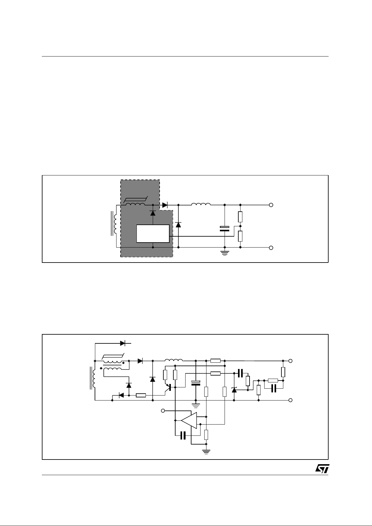
In figure 3, a real example of a mag amp regulator for a 3.3V power rail is shown.
The TL431 acts as a reference voltage/error amplifier. The PNP transistor, driven by the amplified and
frequency-compensated error signal, acts as a controlled current generator that resets the mag amp
core through the auxiliary winding wound on it. The sense resistor Rsense is part of the current limiting
circuit, which includes also the overcurrent comparator with open collector output. The comparator,
when triggered, saturates the reset PNP transistor, thus delaying as much as possible the positive
pulses delivered downstream the reactor and limiting the overcurrent at the output.
Figure 3. Mag amp regulator electrical schematic.
TO THE OUTPUT STA GE
OF THE 5V POWER RAIL
R
sense
MAIN
TRANSFORMER
12 V
+
-
TL431
3.3V
2/6
Page 3

AN1007 APPLICATION NOTE
Without going into details, the problems that arise in such regulators will be here summarized.
To ensure a safe operation also under short circuit conditions with maximum input voltage, the mag amp
core must be overdesigned (typically by 100%). This increases its size, weight and cost.
Furthermore, the switching char acteristics of the magnetic core are not s o good, which lim its the opera-
tional frequency and cause a poor dynamic response of the regulator. This has a negative impact also
on the design of the main transfor mer of the supply and of the primary switch, which will require to be
overdesigned as well.
Both the reactor and the reset PNP exhibit considerable losses, thus the efficiency is not so good.
Another drawback is that the system loses regulation at light output current, thus causing the output volt-
age to drift high. Moreover, if t he regulator starts up with a light load current, the output voltage will experience an overshoot which can be risky for the load. A minimum current consumption (that may be in
the hundred mA) must then be ensured in order to avoid these phenomena. This will require either an
even bigger mag amp core (further size, weight and cost increase) or a dummy load (efficiency will be
hurt) if the output current can go below the minimum value needed to ensure regulation.
Finally, it is not an easy task t o tune a mag amp design so as to achieve a satisfactory behavior in the
whole and, unless the designer has a high level of expertise, it also takes a long time.
On the other hand, mag amp approach has been either the most co mpetitive or the only practicable solution for handling high load currents so far: it avoids the losses inherent in linear regulators and the
complexity of conventional switchers.
L6561-based post regulators
Figure 4 shows an L6561-based post-regulator for generating a 3.3 V power rail, with the same rating as
the one illustrated in fig. 3, running off the winding used for the 5V main output.
Compared to the schematic of fig. 3, the parts count is lower. Moreover, the bulkiest (as well as most expensive) components are replaced by smaller (and cheaper) ones. As a result, the Printed Circuit Board
area that accommodates the L6561-based regulator is very likely to be half the one needed for a similarly rated mag amp-based regulator.
Figure 4. L6561-based switcher for secondary regulation.
TO THE OUTPUT STAGE
OF THE 5V POWER RAIL
Q1
T1
T1
MAIN
TRANSFORMER
DISABLE
R
47 k
10 k
T3
sense
Ω
GD
CS
Ω
ZCD
BC337
The saturable core reactor is r eplaced by a power MOSFET (Q1). Its R
D1
D2
T2
7
4
10 µF
L
o
C
GND
61
L6561
Vcc
Vsupply
o
2
385
820
2.4 k
INV
COMP
MULT
DS(on)
3.3 V
R1
Ω
R2
Ω
D3
1N4148
will be in the ten mΩ, according to the output current rating, in order to minimize conduction losses. Such a low R
involve big and expensive MOSFETs because the lowest V
classes are required.
DSS
DS(on)
does not
3/6
Page 4

AN1007 APPLICATION NOTE
MOSFETs of such low voltage classes are available from ST in TO-220 package for through-hole assemblies and in DPAK / D2PAK packages for surface mount assemblies, as summarized in Table 1.
The table shows the devices suggested for typical output current ratings m entioned in Intel’s Instantly
Available PC (Power Supply ’98) specification.
Table 1. Suggested MOSFETs for typical output current ratings (3.3V output).
I
(A) Part Number (TO-220) Part Number (DPAK) Part Number (D2PAK)
out
6 STP30NE06 55mohm STD20NE06 40mohm - -
8 STP36NE06 40mohm STD20NE06 40mohm - 10 STP55NE06 22mohm - - STB55NE06 22mohm
13 STP80NE06-10 10mohm - - STB80NE06-10 10mohm
Q1 is driven with a gate-drive transformer (T2), with
a coupling capacitor to eliminate the dependence of
the gate-drive voltage on the duty cycle.
The control circuit is based on the L6561, a 8-pin
Transition Mode PFC controller that turns out to be
extremely useful for this application. Please refer to
[1] for a detailed description of the device.
The supply voltage of the L6561 can be got in dif ferent ways, depending on the architecture of the
entire power supply. A couple of examples are
shown in fig. 5.
The oper ation of the circ uit of fig. 4 will b e now described , with the aid of the tim e diagrams sh own in
fig. 6.
Q1 is turned on on the negative edge of the secondary voltage, detected through the ZCD pin, that is
when the primary switch is turned off. The rectifier
D1 withstands the reverse secondary voltage.
The key point is: when Q1 is switched on, the current through D1 and Q1 is zero, thus Q1 does not
experience any switching loss and the reverse recovery of D1 is here of no concern.
When the primary switch is turned on, the secondary voltage becomes positive and, being Q1 already on, D1 conducts. The secondary voltage (reduced by D1 forward drop) minus the output voltage
is applied to the output inductor Lo, causing the inductor current to ramp up.
A current-sense transformer (T3) picks up the inductor current (flowing through Q1 as well) and develops a voltage on R
proportional to the cur-
sense
rent. This voltage, applied to CS pin, is internally
compared to the output of the multiplier of the
L6561 and when the two quantities are equal , Q1 is
switched off. The system performs ther efore a trailing edge modulation.
The multiplier output voltage is proportional to the
product of the error amplifier output voltage (at pin
COMP) times the multiplier input voltage (at pin
MULT). COMP voltage is in turn a function of the
amplified difference between a por tion of the output
voltage (set by R1 and R2) and the internal 2.5V
Figure 5. Circuits for the generation of the
L6561 supply voltage
V
supply
(13 < V < 18)
5V
OUTPUT
12V / 4 A
MAIN
L4955
V
supply
TO FEEDBACK
Figure 6. L6561-based switcher time diagrams.
PRIMARY
SWITCH
SECONDARY
VOLT AGE
Q1 GATE
VOLT AGE
Q1 & D1
CURRENT
D2
CURRENT
ONOFF
4/6
Page 5

AN1007 APPLICATION NOTE
(±1% @ Tj = 25°C) voltage reference.
VMUL voltage is connected to the output voltage, in this way providing foldback current limiting. This
function provides a short circuit c urrent lower then the nor mal load current, thus gr eatly reducing the
stress on the power components in case of failure.
The diode D3 avoids latchoff, that is prevents the output current from dropping to zero during short circuits and staying at zero even when the short circuit is removed. Furthermore, at start-up, there is a softstart action because of the limitation of the current inflow.
The regulator will exhibit a better ef ficiency over its mag am p counterpart: the dissipation on the MOSFET is quite limited (about 1W with the parts suggested in Tab.1), while the mag amp dissipates on the
copper and the core of the reactor, as well as some hundreds mW on the reset PNP transistor.
The "peak" current mode control performed by the circuit offers many more benefits: excellent load regulation from very low output current up to the maximum load, fast response to step-load changes, good
line regulation due to the inherent input voltage feedforward and one-pole transfer function of the output
stage, which simplifies frequency compensation.
Additionally, since the L6561 can be disabled by grounding the ZCD pin, t he entire regulator can be
either enabled or shut down with a logic signal. Besides, being the L6561 on the secondary side, the interface needed to feed the enable/disable signal will be extremely simple, like the one shown in the
schematic of fig. 4.
This disable feature achieves a real zero-power s hutdown. In fact, when the regulator is disabled, Q1 is
kept off and the secondary winding is an open circuit . The only power consumption is a couple of mA
from the supply pin of the L6561.
This functionality turns out to be extremely useful in those systems were power management is required,
as stated in Intel’s Power Supply ’98 specifications, for example.
Conclusions
The replacement of a mag amp-based post regulator with an L6561-based one for the generation of a
given auxiliary power rail allows to save numerous external parts among which the bulky and expensive
mag amp core. Such a regulator will benefit a dramatic cost reduction from the lower number and cost of
the parts used, from the shrinkage of the PCB area needed to accommodate the circuit and from a cut of
the design time.
In spite of t hat, the result is a much more performant system which take s advantage of all the benefits
inherent in switching regulation with current mode control as well as of the functionalities available from
the versatile L6561.
REFERENCE
[1] "L6561, Enhanced Transition Mode Power Factor Corrector" (AN966)
5/6
Page 6

AN1007 APPLICATION NOTE
Information furnished is believ ed to be accura te an d rel i abl e. However, STM i croelectronics ass um es no responsibil ity for the consequences
of use of such informati on nor for any infringement of patents or other ri ghts of third parties which may result from its use. No license is
granted by implication or other wis e under any patent or patent rights of STMi croelec tronics. Spec ifications mention ed in this p ublicatio n are
subject to c hange without notice. T hi s publication supersedes and replac es all information previously su ppl ie d. S TMicroelectronics products
are not authorized for use as critical components in life support devices or systems without express written approval of STMicroelectronics.
The ST logo is a registered trademark of STMicroelectronics.
All other names are the property of their respective owners
© 2003 STMicroelectronics - All rights reser ved
STMicroelectron ics GROUP OF COMPA NI ES
Australia – Belgium - Brazil - Canada - China – Czech Republic - Finland - France - Germany - Hong Kong - India - Israel - Italy - Japan -
Malaysia - Malta - Morocco - Singapore - Spain - Sweden - Switzerland - United Kingdom - United States
www.st.com
6/6
 Loading...