How it Works
Log In / Sign Up
Buy Points
How it Works
FAQ
Contact Us
Questions and Suggestions
Users
ST
Loading...
#
74VHCT04A
74VHCT08A
74VHCT125A
74VHCT138A
74VHCT238A
74VHCT244A
74VHCT245A
74VHCT273A
74VHCT32A
74VHCT541A
74VHCT573A
74VHCT574A
74VHCU04
A
A1-lite
A3G4250D
A5970AD
A5970D
A5972D
A5973AD
A5973D
A5974AD
A5974D
A5975AD
A6902D
A7985A
A7986A
AC7MDT10-D20
AC7MDT10-D32
AC7MDT10S20
AC7MDT10-S28
ACS102-6T
ACS108
ACS108-6S
ACS110-7SB2
ACS110-7SN
ACS120-7SB
ACS120-7SFP
ACS120-7ST
ACS302-5T3
ACST10
ACST12
ACST2
ACST4
ACST6
ACST8
AD-ICD
AEKD-USBTYPEC1
AFM 1.0
AIS326DQ
AIS328DQ
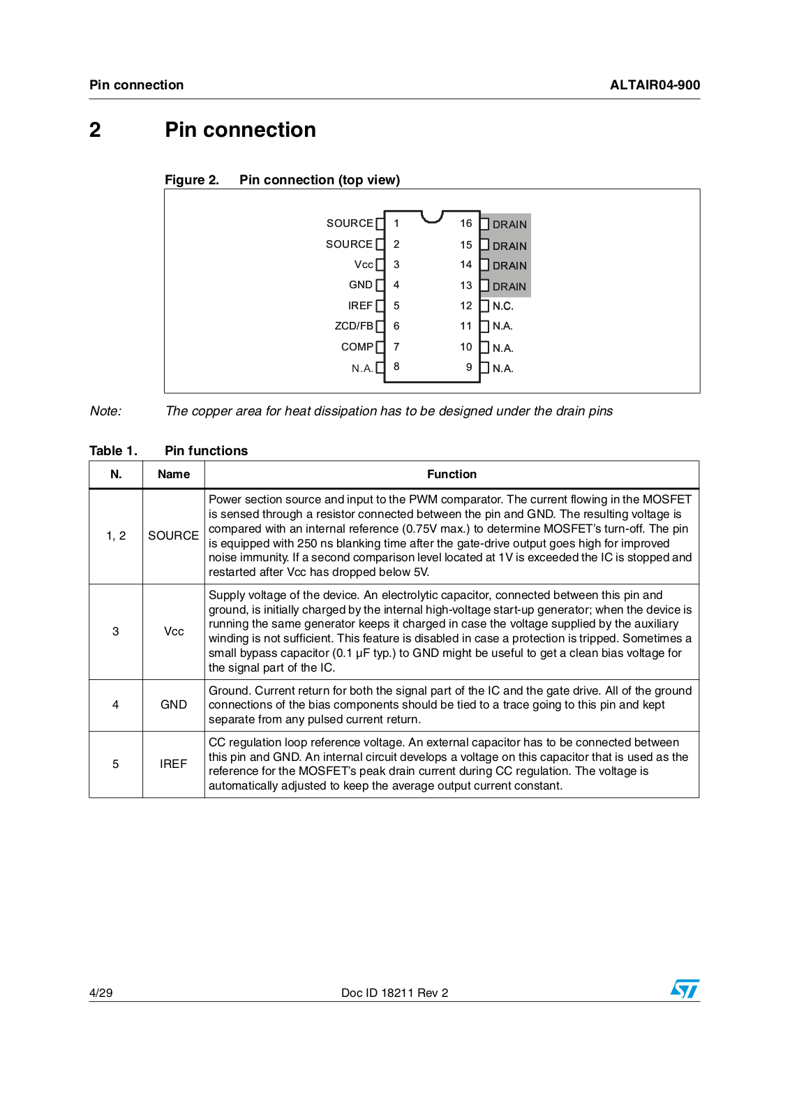
ALTAIR04-900
ALTAIR05T-800
AM83135-015
AN1000
AN1007
AN1009
AN1012
AN1014
AN1019
AN1021
AN1042
AN1045
AN1048
AN1049
AN1051
AN1059
AN1060
AN1061
AN1070
AN1088
AN1089
AN1094
AN1105
AN1126
AN1132
AN1172
AN1213
AN1214
AN1215
AN1216
AN1220
AN1223
AN1224
AN1226
AN1228
AN1229
AN1230
AN1232
AN1233
AN1235
AN1246
AN1256
AN1278
AN1281
AN1282
AN1283
AN1284
AN1294
AN1296
AN 2119
Loading...
Loading...
Nothing found
ALTAIR04-900
User Manual
29 pgs
649.45 Kb
0
Table of contents
Loading...
ST ALTAIR04-900 User Manual
...
ST User Manual
Download
Specifications and Main Features
Frequently Asked Questions
User Manual
Download
Loading...
+
hidden pages
Unhide
You need points to download manuals.
1 point = 1 manual.
You can buy points or you can get point for every manual you upload.
Buy points
Upload your manuals
 Loading...