

AIS328DQ
QFN 24
(4 x 4 x 1.8 mm3)
High-performance ultra low-power 3-axis accelerometer with digital
output for automotive applications
Datasheet — production data
Features
■ Wide supply voltage range: 2.4 V to 3.6 V
■ Low voltage compatible IOs: 1.8 V
■ Ultra low-power mode consumption: down to
10 µA
■ ±2g/±4g/±8g dynamically selectable full-scale
■ SPI / I
■ 16-bit data output
■ 2 independent programmable interrupt
■ System sleep/wakeup function
■ Extended temperature range: -40 °C to 105 °C
■ Embedded self-test
■ High shock survivability: up to 10000 g
■ ECOPACK
■ AEC-Q100 qualification
Applications
■ Telematics and black boxes
■ In-dash car navigation
■ Tilt / inclination measurement
■ Anti-theft devices
■ Intelligent power saving
■ Impact recognition and logging
■ Vibration monitoring and compensation
■ Motion-activated functions
Table 1. Device summary
2
C digital output interface
generators
®
RoHS and “Green” compliant
Description
The AIS328DQ is an ultra low-power high
performance 3-axis linear accelerometer with a
digital serial interface SPI standard output. An I
compatible interface is also available. The device
features ultra low-power operational modes that
allow advanced power saving and smart sleep-towakeup functions. The AIS328DQ has dynamic
user-selectable full-scales of ±2g/±4g/±8g and is
capable of measuring accelerations with output
data rates from 0.5 Hz to 1 kHz. The self-test
capability allows the user to check the functioning
of the sensor in the final application. The device
may be configured to generate an interrupt signal
through inertial wakeup events, or by the position
of the device itself. Thresholds and the timing of
interrupt generators are programmable by the end
user on-the-fly. Available in a small quad flat pack
no-lead package (QFPN) with a 4x4 mm footprint,
the AIS328DQ is able to respond to the trend
towards application miniaturization, and is
guaranteed to operate over a temperature range
from -40 °C to +105 °C.
2
C
Order codes Temperature range [°C] Package Packaging
AIS328DQ -40 to +105 QFPN 4x4x1.8 24L Tray
AIS328DQTR -40 to +105 QFPN 4x4x1.8 24L Tape and reel
April 2012 Doc ID 18160 Rev 3 1/43
This is information on a product in full production.
www.st.com
43

Contents AIS328DQ
Contents
1 Block diagram and pin description . . . . . . . . . . . . . . . . . . . . . . . . . . . . . 6
1.1 Block diagram . . . . . . . . . . . . . . . . . . . . . . . . . . . . . . . . . . . . . . . . . . . . . . . 6
1.2 Pin description . . . . . . . . . . . . . . . . . . . . . . . . . . . . . . . . . . . . . . . . . . . . . . 6
2 Mechanical and electrical specifications . . . . . . . . . . . . . . . . . . . . . . . . 8
2.1 Mechanical characteristics . . . . . . . . . . . . . . . . . . . . . . . . . . . . . . . . . . . . . 8
2.2 Electrical characteristics . . . . . . . . . . . . . . . . . . . . . . . . . . . . . . . . . . . . . . . 9
2.3 Communication interface characteristics . . . . . . . . . . . . . . . . . . . . . . . . . 10
2.3.1 SPI - serial peripheral interface . . . . . . . . . . . . . . . . . . . . . . . . . . . . . . . 10
2.3.2 I²C - inter IC control interface . . . . . . . . . . . . . . . . . . . . . . . . . . . . . . . . . 11
2.4 Absolute maximum ratings . . . . . . . . . . . . . . . . . . . . . . . . . . . . . . . . . . . . 12
2.5 Terminology . . . . . . . . . . . . . . . . . . . . . . . . . . . . . . . . . . . . . . . . . . . . . . . 13
2.5.1 Sensitivity . . . . . . . . . . . . . . . . . . . . . . . . . . . . . . . . . . . . . . . . . . . . . . . . 13
2.5.2 Zero-g level . . . . . . . . . . . . . . . . . . . . . . . . . . . . . . . . . . . . . . . . . . . . . . 13
2.5.3 Self-test . . . . . . . . . . . . . . . . . . . . . . . . . . . . . . . . . . . . . . . . . . . . . . . . . 13
2.5.4 Sleep-to-wakeup . . . . . . . . . . . . . . . . . . . . . . . . . . . . . . . . . . . . . . . . . . 14
3 Functionality . . . . . . . . . . . . . . . . . . . . . . . . . . . . . . . . . . . . . . . . . . . . . . 15
3.1 Sensing element . . . . . . . . . . . . . . . . . . . . . . . . . . . . . . . . . . . . . . . . . . . . 15
3.2 IC interface . . . . . . . . . . . . . . . . . . . . . . . . . . . . . . . . . . . . . . . . . . . . . . . . 15
3.3 Factory calibration . . . . . . . . . . . . . . . . . . . . . . . . . . . . . . . . . . . . . . . . . . 15
4 Application hints . . . . . . . . . . . . . . . . . . . . . . . . . . . . . . . . . . . . . . . . . . . 16
5 Digital interfaces . . . . . . . . . . . . . . . . . . . . . . . . . . . . . . . . . . . . . . . . . . . 17
5.1 I²C serial interface . . . . . . . . . . . . . . . . . . . . . . . . . . . . . . . . . . . . . . . . . . 17
5.1.1 I²C operation . . . . . . . . . . . . . . . . . . . . . . . . . . . . . . . . . . . . . . . . . . . . . 18
5.2 SPI bus interface . . . . . . . . . . . . . . . . . . . . . . . . . . . . . . . . . . . . . . . . . . . 19
5.2.1 SPI read . . . . . . . . . . . . . . . . . . . . . . . . . . . . . . . . . . . . . . . . . . . . . . . . . 20
5.2.2 SPI write . . . . . . . . . . . . . . . . . . . . . . . . . . . . . . . . . . . . . . . . . . . . . . . . 21
5.2.3 SPI read in 3-wire mode . . . . . . . . . . . . . . . . . . . . . . . . . . . . . . . . . . . . 22
6 Register mapping . . . . . . . . . . . . . . . . . . . . . . . . . . . . . . . . . . . . . . . . . . 23
2/43 Doc ID 18160 Rev 3

AIS328DQ Contents
7 Register description . . . . . . . . . . . . . . . . . . . . . . . . . . . . . . . . . . . . . . . . 25
7.1 WHO_AM_I (0Fh) . . . . . . . . . . . . . . . . . . . . . . . . . . . . . . . . . . . . . . . . . . . 25
7.2 CTRL_REG1 (20h) . . . . . . . . . . . . . . . . . . . . . . . . . . . . . . . . . . . . . . . . . . 25
7.3 CTRL_REG2 (21h) . . . . . . . . . . . . . . . . . . . . . . . . . . . . . . . . . . . . . . . . . . 26
7.4 CTRL_REG3 [Interrupt CTRL register] (22h) . . . . . . . . . . . . . . . . . . . . . . 27
7.5 CTRL_REG4 (23h) . . . . . . . . . . . . . . . . . . . . . . . . . . . . . . . . . . . . . . . . . . 28
7.6 CTRL_REG5 (24h) . . . . . . . . . . . . . . . . . . . . . . . . . . . . . . . . . . . . . . . . . . 29
7.7 HP_FILTER_RESET (25h) . . . . . . . . . . . . . . . . . . . . . . . . . . . . . . . . . . . . 29
7.8 REFERENCE (26h) . . . . . . . . . . . . . . . . . . . . . . . . . . . . . . . . . . . . . . . . . 30
7.9 STATUS_REG (27h) . . . . . . . . . . . . . . . . . . . . . . . . . . . . . . . . . . . . . . . . . 30
7.10 OUT_X_L (28h), OUT_X_H (29) . . . . . . . . . . . . . . . . . . . . . . . . . . . . . . . 31
7.11 OUT_Y_L (2Ah), OUT_Y_H (2Bh) . . . . . . . . . . . . . . . . . . . . . . . . . . . . . . 31
7.12 OUT_Z_L (2Ch), OUT_Z_H (2Dh) . . . . . . . . . . . . . . . . . . . . . . . . . . . . . . 31
7.13 INT1_CFG (30h) . . . . . . . . . . . . . . . . . . . . . . . . . . . . . . . . . . . . . . . . . . . . 31
7.14 INT1_SRC (31h) . . . . . . . . . . . . . . . . . . . . . . . . . . . . . . . . . . . . . . . . . . . . 32
7.15 INT1_THS(32h) . . . . . . . . . . . . . . . . . . . . . . . . . . . . . . . . . . . . . . . . . . . . 32
7.16 INT1_DURATION (33h) . . . . . . . . . . . . . . . . . . . . . . . . . . . . . . . . . . . . . . 33
7.17 INT2_CFG (34h) . . . . . . . . . . . . . . . . . . . . . . . . . . . . . . . . . . . . . . . . . . . . 33
7.18 INT2_SRC (35h) . . . . . . . . . . . . . . . . . . . . . . . . . . . . . . . . . . . . . . . . . . . . 34
7.19 INT2_THS (36h) . . . . . . . . . . . . . . . . . . . . . . . . . . . . . . . . . . . . . . . . . . . . 34
7.20 INT2_DURATION (37h) . . . . . . . . . . . . . . . . . . . . . . . . . . . . . . . . . . . . . . 35
8 Package information . . . . . . . . . . . . . . . . . . . . . . . . . . . . . . . . . . . . . . . . 36
9 Soldering information . . . . . . . . . . . . . . . . . . . . . . . . . . . . . . . . . . . . . . . 38
9.1 General guidelines about soldering surface-mounted accelerometers . . 38
9.2 PCB design guidelines . . . . . . . . . . . . . . . . . . . . . . . . . . . . . . . . . . . . . . . 38
9.2.1 PCB design rules . . . . . . . . . . . . . . . . . . . . . . . . . . . . . . . . . . . . . . . . . . 39
9.3 Stencil design and solder paste application . . . . . . . . . . . . . . . . . . . . . . . 39
9.4 Process considerations . . . . . . . . . . . . . . . . . . . . . . . . . . . . . . . . . . . . . . 40
10 Revision history . . . . . . . . . . . . . . . . . . . . . . . . . . . . . . . . . . . . . . . . . . . 41
Doc ID 18160 Rev 3 3/43

List of tables AIS328DQ
List of tables
Table 1. Device summary . . . . . . . . . . . . . . . . . . . . . . . . . . . . . . . . . . . . . . . . . . . . . . . . . . . . . . . . . . 1
Table 2. Pin description . . . . . . . . . . . . . . . . . . . . . . . . . . . . . . . . . . . . . . . . . . . . . . . . . . . . . . . . . . . 7
Table 3. Mechanical characteristics . . . . . . . . . . . . . . . . . . . . . . . . . . . . . . . . . . . . . . . . . . . . . . . . . . 8
Table 4. Electrical characteristics . . . . . . . . . . . . . . . . . . . . . . . . . . . . . . . . . . . . . . . . . . . . . . . . . . . . 9
Table 5. SPI slave timing values. . . . . . . . . . . . . . . . . . . . . . . . . . . . . . . . . . . . . . . . . . . . . . . . . . . . 10
Table 6. I²C slave timing values . . . . . . . . . . . . . . . . . . . . . . . . . . . . . . . . . . . . . . . . . . . . . . . . . . . . 11
Table 7. Absolute maximum ratings . . . . . . . . . . . . . . . . . . . . . . . . . . . . . . . . . . . . . . . . . . . . . . . . . 12
Table 8. Serial interface pin description . . . . . . . . . . . . . . . . . . . . . . . . . . . . . . . . . . . . . . . . . . . . . . 17
Table 9. Serial interface pin description . . . . . . . . . . . . . . . . . . . . . . . . . . . . . . . . . . . . . . . . . . . . . . 17
Table 10. SAD+Read/Write patterns . . . . . . . . . . . . . . . . . . . . . . . . . . . . . . . . . . . . . . . . . . . . . . . . . 18
Table 11. Transfer when master is writing one byte to slave . . . . . . . . . . . . . . . . . . . . . . . . . . . . . . . 18
Table 12. Transfer when master is writing multiple bytes to slave . . . . . . . . . . . . . . . . . . . . . . . . . . . 18
Table 13. Transfer when master is receiving (reading) one byte of data from slave . . . . . . . . . . . . . 19
Table 14. Transfer when master is receiving (reading) multiple bytes of data from slave . . . . . . . . . 19
Table 15. Register address map. . . . . . . . . . . . . . . . . . . . . . . . . . . . . . . . . . . . . . . . . . . . . . . . . . . . . 23
Table 16. WHO_AM_I register . . . . . . . . . . . . . . . . . . . . . . . . . . . . . . . . . . . . . . . . . . . . . . . . . . . . . . 25
Table 17. CTRL_REG1 register . . . . . . . . . . . . . . . . . . . . . . . . . . . . . . . . . . . . . . . . . . . . . . . . . . . . . 25
Table 18. CTRL_REG1 description . . . . . . . . . . . . . . . . . . . . . . . . . . . . . . . . . . . . . . . . . . . . . . . . . . 25
Table 19. Power mode and low-power output data rate configurations . . . . . . . . . . . . . . . . . . . . . . . 26
Table 20. Normal-mode output data rate configurations and low-pass cut-off frequencies . . . . . . . . 26
Table 21. CTRL_REG2 register . . . . . . . . . . . . . . . . . . . . . . . . . . . . . . . . . . . . . . . . . . . . . . . . . . . . . 26
Table 22. CTRL_REG2 description . . . . . . . . . . . . . . . . . . . . . . . . . . . . . . . . . . . . . . . . . . . . . . . . . . 26
Table 23. High-pass filter mode configuration . . . . . . . . . . . . . . . . . . . . . . . . . . . . . . . . . . . . . . . . . . 27
Table 24. High-pass filter cut-off frequency configuration . . . . . . . . . . . . . . . . . . . . . . . . . . . . . . . . . 27
Table 25. CTRL_REG3 register . . . . . . . . . . . . . . . . . . . . . . . . . . . . . . . . . . . . . . . . . . . . . . . . . . . . . 27
Table 26. CTRL_REG3 description . . . . . . . . . . . . . . . . . . . . . . . . . . . . . . . . . . . . . . . . . . . . . . . . . . 28
Table 27. Data signal on INT 1 and INT 2 pad . . . . . . . . . . . . . . . . . . . . . . . . . . . . . . . . . . . . . . . . . . 28
Table 28. CTRL_REG4 register . . . . . . . . . . . . . . . . . . . . . . . . . . . . . . . . . . . . . . . . . . . . . . . . . . . . . 28
Table 29. CTRL_REG4 description . . . . . . . . . . . . . . . . . . . . . . . . . . . . . . . . . . . . . . . . . . . . . . . . . . 28
Table 30. CTRL_REG5 register . . . . . . . . . . . . . . . . . . . . . . . . . . . . . . . . . . . . . . . . . . . . . . . . . . . . . 29
Table 31. CTRL_REG5 description . . . . . . . . . . . . . . . . . . . . . . . . . . . . . . . . . . . . . . . . . . . . . . . . . . 29
Table 32. Sleep-to-wake configuration . . . . . . . . . . . . . . . . . . . . . . . . . . . . . . . . . . . . . . . . . . . . . . . . 29
Table 33. REFERENCE register. . . . . . . . . . . . . . . . . . . . . . . . . . . . . . . . . . . . . . . . . . . . . . . . . . . . . 30
Table 34. REFERENCE description . . . . . . . . . . . . . . . . . . . . . . . . . . . . . . . . . . . . . . . . . . . . . . . . . . 30
Table 35. STATUS_REG register . . . . . . . . . . . . . . . . . . . . . . . . . . . . . . . . . . . . . . . . . . . . . . . . . . . . 30
Table 36. STATUS_REG description . . . . . . . . . . . . . . . . . . . . . . . . . . . . . . . . . . . . . . . . . . . . . . . . . 30
Table 37. INT1_CFG register . . . . . . . . . . . . . . . . . . . . . . . . . . . . . . . . . . . . . . . . . . . . . . . . . . . . . . . 31
Table 38. INT1_CFG description . . . . . . . . . . . . . . . . . . . . . . . . . . . . . . . . . . . . . . . . . . . . . . . . . . . . 31
Table 39. Interrupt 1 source configurations . . . . . . . . . . . . . . . . . . . . . . . . . . . . . . . . . . . . . . . . . . . . 32
Table 40. INT1_SRC register . . . . . . . . . . . . . . . . . . . . . . . . . . . . . . . . . . . . . . . . . . . . . . . . . . . . . . . 32
Table 41. INT1_SRC description . . . . . . . . . . . . . . . . . . . . . . . . . . . . . . . . . . . . . . . . . . . . . . . . . . . . 32
Table 42. INT1_THS register . . . . . . . . . . . . . . . . . . . . . . . . . . . . . . . . . . . . . . . . . . . . . . . . . . . . . . . 32
Table 43. INT1_THS description . . . . . . . . . . . . . . . . . . . . . . . . . . . . . . . . . . . . . . . . . . . . . . . . . . . . 33
Table 44. INT1_DURATION register . . . . . . . . . . . . . . . . . . . . . . . . . . . . . . . . . . . . . . . . . . . . . . . . . 33
Table 45. INT2_DURATION description . . . . . . . . . . . . . . . . . . . . . . . . . . . . . . . . . . . . . . . . . . . . . . . 33
Table 46. INT2_CFG register . . . . . . . . . . . . . . . . . . . . . . . . . . . . . . . . . . . . . . . . . . . . . . . . . . . . . . . 33
Table 47. INT2_CFG description . . . . . . . . . . . . . . . . . . . . . . . . . . . . . . . . . . . . . . . . . . . . . . . . . . . . 33
Table 48. Interrupt mode configuration . . . . . . . . . . . . . . . . . . . . . . . . . . . . . . . . . . . . . . . . . . . . . . . . 34
4/43 Doc ID 18160 Rev 3

AIS328DQ List of tables
Table 49. INT2_SRC register . . . . . . . . . . . . . . . . . . . . . . . . . . . . . . . . . . . . . . . . . . . . . . . . . . . . . . . 34
Table 50. INT2_SRC description . . . . . . . . . . . . . . . . . . . . . . . . . . . . . . . . . . . . . . . . . . . . . . . . . . . . 34
Table 51. INT2_THS register . . . . . . . . . . . . . . . . . . . . . . . . . . . . . . . . . . . . . . . . . . . . . . . . . . . . . . . 34
Table 52. INT2_THS description . . . . . . . . . . . . . . . . . . . . . . . . . . . . . . . . . . . . . . . . . . . . . . . . . . . . 35
Table 53. INT2_DURATION register . . . . . . . . . . . . . . . . . . . . . . . . . . . . . . . . . . . . . . . . . . . . . . . . . 35
Table 54. INT2_DURATION description . . . . . . . . . . . . . . . . . . . . . . . . . . . . . . . . . . . . . . . . . . . . . . . 35
Table 55. Document revision history . . . . . . . . . . . . . . . . . . . . . . . . . . . . . . . . . . . . . . . . . . . . . . . . . 41
Doc ID 18160 Rev 3 5/43

List of figures AIS328DQ
List of figures
Figure 1. Block diagram . . . . . . . . . . . . . . . . . . . . . . . . . . . . . . . . . . . . . . . . . . . . . . . . . . . . . . . . . . . . 7
Figure 2. Detectable accelerations and pin indicator . . . . . . . . . . . . . . . . . . . . . . . . . . . . . . . . . . . . . . 7
Figure 3. SPI slave timing diagram (2). . . . . . . . . . . . . . . . . . . . . . . . . . . . . . . . . . . . . . . . . . . . . . . . 12
Figure 4. I²C slave timing diagram . . . . . . . . . . . . . . . . . . . . . . . . . . . . . . . . . . . . . . . . . . . . . . . . . . 13
Figure 5. AIS328DQ electrical connections . . . . . . . . . . . . . . . . . . . . . . . . . . . . . . . . . . . . . . . . . . . . 17
Figure 6. Read and write protocol . . . . . . . . . . . . . . . . . . . . . . . . . . . . . . . . . . . . . . . . . . . . . . . . . . . 20
Figure 7. SPI read protocol . . . . . . . . . . . . . . . . . . . . . . . . . . . . . . . . . . . . . . . . . . . . . . . . . . . . . . . . 21
Figure 8. Multiple byte SPI read protocol (2-byte example) . . . . . . . . . . . . . . . . . . . . . . . . . . . . . . . . 22
Figure 9. SPI write protocol . . . . . . . . . . . . . . . . . . . . . . . . . . . . . . . . . . . . . . . . . . . . . . . . . . . . . . . . 22
Figure 10. Multiple bytes SPI write protocol (2-byte example). . . . . . . . . . . . . . . . . . . . . . . . . . . . . . . 22
Figure 11. SPI read protocol in 3-wire mode . . . . . . . . . . . . . . . . . . . . . . . . . . . . . . . . . . . . . . . . . . . . 23
Figure 12. QFPN 4x4x1.8mm
Figure 13. Recommended land and solder mask design for QFPN packages . . . . . . . . . . . . . . . . . . 40
3
, 24L: mechanical data and package dimensions . . . . . . . . . . . . . . . . 38
6/43 Doc ID 18160 Rev 3
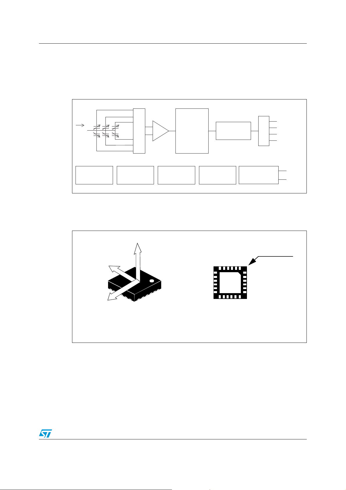
AIS328DQ Block diagram and pin description
Y+
Z+
Y-
Z
-
a
X+
X-
I2C
SPI
CS
SCL/SPC
SDA/SDO/SDI
SDO/SA0
CONTROL LOGIC
INTERRUPT GEN.
INT 1
CLOCK
TRIMMING
CIRCUITS
REFERENCESELF TEST
CONTROL
LOGIC
ADC
INT 2
MUX
CHARGE
AMPLIFIER
AM10246V1
(TOP VIEW)
DIRECTION OF THE
DETECTABLE
ACCELERATIONS
(BOTTOM VIEW)
Y
1
X
Z
Pin 1 indicator
1
6
13
18
7
12
19 24
1 Block diagram and pin description
1.1 Block diagram
Figure 1. Block diagram
1.2 Pin description
Figure 2. Detectable accelerations and pin indicator
Doc ID 18160 Rev 3 7/43
Block diagram and pin description AIS328DQ
Table 2. Pin description
Pin# Name Function
1,2 NC Not connected
3 INT_2 Inertial interrupt 2
4 Reserved Connect to GND
5 VDD Power supply
6 GND 0 V supply
7 INT_1 Inertial interrupt 1
8 GND 0 V supply
9 GND 0 V supply
10 GND 0 V supply
SPI serial port clock (SPC)
I²C serial clock (SCL)
Internal active pull-up
11
SPC
SCL
SPI enable
12 CS
I²C/SPI mode selection (0: SPI enabled; 1: I²C mode)
Internal active pull-up
13 Reserved Connect to Vdd
14 VDD_IO Power supply for I/O pins
SPI serial data output (SDO)
I²C less significant bit of the device address (SA0)
Internal active pull-up
SPI serial data input (SDI)
3-wire interface serial data output (SDO)
I²C serial data (SDA)
Internal active pull-up
15
16
SDO
SA0
SDI
SDO
SDA
17-24 NC Not internally connected
8/43 Doc ID 18160 Rev 3
AIS328DQ Mechanical and electrical specifications
2 Mechanical and electrical specifications
2.1 Mechanical characteristics
@ Vdd=3.3 V, T=-40 °C to +105 °C unless otherwise noted
Table 3. Mechanical characteristics
Symbol Parameter Test conditions Min. Typ.
FS bit set to 00 ±2.0
FS Measurement range
So Sensitivity
Off
Ty Of f
TCOff
Zero-g level offset
accuracy
Ty p i c a l z e ro - g level offset
accuracy
(3),(4),(5)
(5),(6)
Zero-g level change vs.
temperature
An Acceleration noise density FS bit set to 00 100 218 600 µg/
CrAx Cross-axis
Vst
Self-test output
change
(7)
(8),(9),(10)
Wh Product weight 60 mgram
Top Operating temperature range -40 +105 °C
1. Typical values are not guaranteed.
2. Verified by wafer level test and measurement of initial offset and sensitivity.
3. Zero-g level offset value after MSL3 preconditioning.
4. Zero-g level offset at the FS bit set to 01 and 11 is guaranteed by design.
(2)
FS bit set to 11 ±8.0
FS bit set to 00
12-bit representation
FS bit set to 01
12-bit representation
FS bit set to 11
12-bit representation
X,Y axes -200 200
Z-axis -300 300
FS bit set to 00 -30 ±20 30 mg
Excursion from 25 °C (X, Y
axes)
Excursion from 25 °C (Zaxis)
FS bit set to 00
X-axis
FS bit set to 00
Y- a x i s
FS bit set to 00
Z-axis
(a)
.
(1)
Max. Unit
gFS bit set to 01 ±4.0
0.90 0.98 1.06
1.81 1.95 2.12
mg/digit
3.62 3.91 4.25
mg
-2 ±0.2 2
mg/°C
-3 ±0.8 3
√Hz
-5 +5 %
-500 -800 -1100 LSb
500 800 1100 LSb
400 600 800 LSb
a. The product is factory calibrated at 3.3 V. Operational power supply (Vdd) over 3.6 V is not recommended.
Doc ID 18160 Rev 3 9/43
Mechanical and electrical specifications AIS328DQ
5. Offset can be eliminated by enabling the built-in high-pass filter.
6. Typical zero-g level offset as per factory calibration @ T = 25
7. Guaranteed by design.
8. The sign of “Self-test output change” is defined by a sign bit, for all axes. Values in Table 3 are defined with the STsign bit
in the CTRL_REG4 register equal to logic “0” (positive self-test), at T = 25 °C.
Self-test output changes with the power supply. “Self-test output change” is defined as
9.
OUTPUT[LSb]
scale.
10. Output data reaches 99% of final value after 3/ODR when enabling self-test mode, due to device filtering.
(CTRL_REG4 ST bit=1)
- OUTPUT[LSb]
(CTRL_REG4 ST bit=0)
°C.
. 1LSb=4g/4096 at 12-bit representation, ±2 g full-
2.2 Electrical characteristics
@ Vdd = 3.3 V, T = -40 °C to +105 °C unless otherwise noted
Table 4. Electrical characteristics
Symbol Parameter Test conditions Min. Typ
Vdd Supply voltage 2.4 3.3 3.6 V
Vdd_IO I/O pins supply voltage
Idd
Current consumption
in normal mode
(2)
1.8 Vdd+0.1 V
2.4 V to 3.6 V 200 450 µA
(b)
.
(1)
.Max.Unit
IddLP
IddPdn
VIH
Current consumption
in low-power mode
Current consumption in
power-down mode
Digital high level input
voltage
ODR=1 Hz, BW=500
Hz, T=25 °C
81012µA
0.1 1 2 µA
0.8*Vdd_IO V
VIL Digital low level input voltage 0.2*Vdd_IO V
VOH High level output voltage 0.9*Vdd_IO V
VOL Low level output voltage 0.1*Vdd_IO V
DR bit set to 00 50
ODR
Output data rate
in normal mode
DR bit set to 01 100
DR bit set to 10 400
DR bit set to 11 1000
PM bit set to 010 0.5
PM bit set to 011 1
ODR
Output data rate
LP
in low-power mode
PM bit set to 100 2
PM bit set to 101 5
PM bit set to 110 10
Hz
Hz
b. The product is factory calibrated at 3.3 V. Operational power supply (Vdd) over 3.6 V is not recommended.
10/43 Doc ID 18160 Rev 3
AIS328DQ Mechanical and electrical specifications
Table 4. Electrical characteristics (continued)
Symbol Parameter Test conditions Min. Typ
BW System bandwidth ODR/2 Hz
(1)
.Max.Unit
Ton Turn-on time
(3)
ODR = 100 Hz
0.9/ODR
+1 ms
1/ODR+1 ms
1.1/ODR
+1 ms
Top Operating temperature range -40 +105
1. Typical values are not guaranteed.
2. It is possible to remove Vdd maintaining Vdd_IO without blocking the communication busses; in this condition the
measurement chain is powered off.
3. Time to obtain valid data after exiting power-down mode.
2.3 Communication interface characteristics
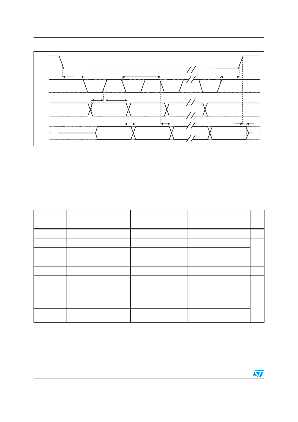
2.3.1 SPI - serial peripheral interface
Subject to general operating conditions for Vdd and Top.
Table 5. SPI slave timing values
(1)
Val ue
Symbol Parameter
Min. Max.
tc(SPC) SPI clock cycle 100 ns
fc(SPC) SPI clock frequency 10 MHz
tsu(CS) CS setup time 6
th(CS) CS hold time 8
s
°C
Unit
tsu(SI) SDI input setup time 5
th(SI) SDI input hold time 15
tv(SO) SDO valid output time 50
th(SO) SDO output hold time 9
tdis(SO) SDO output disable time 50
Doc ID 18160 Rev 3 11/43
ns
Mechanical and electrical specifications AIS328DQ
SPC
CS
SDI
SDO
t
su(CS)
t
v(SO)
t
h(SO)
t
h(SI)
t
su(SI)
t
h(CS)
t
dis(SO)
t
c(SPC)
MSB IN
MSB OUT
LSB OUT
LSB IN
(3)
(3)
(3)
(3)
(3)
(3)
(3)
(3)
(2)
Figure 3. SPI slave timing diagram
1. Values are guaranteed at 10 MHz clock frequency for SPI with both 4 and 3 wires, based on characterization results, not
tested in production.
2. Measurement points are made at 0.2·Vdd_IO and 0.8·Vdd_IO, for both input and output ports.
3. When no communication is ongoing, data on CS, SPC, SDI and SDO are driven by internal pull-up resistors.
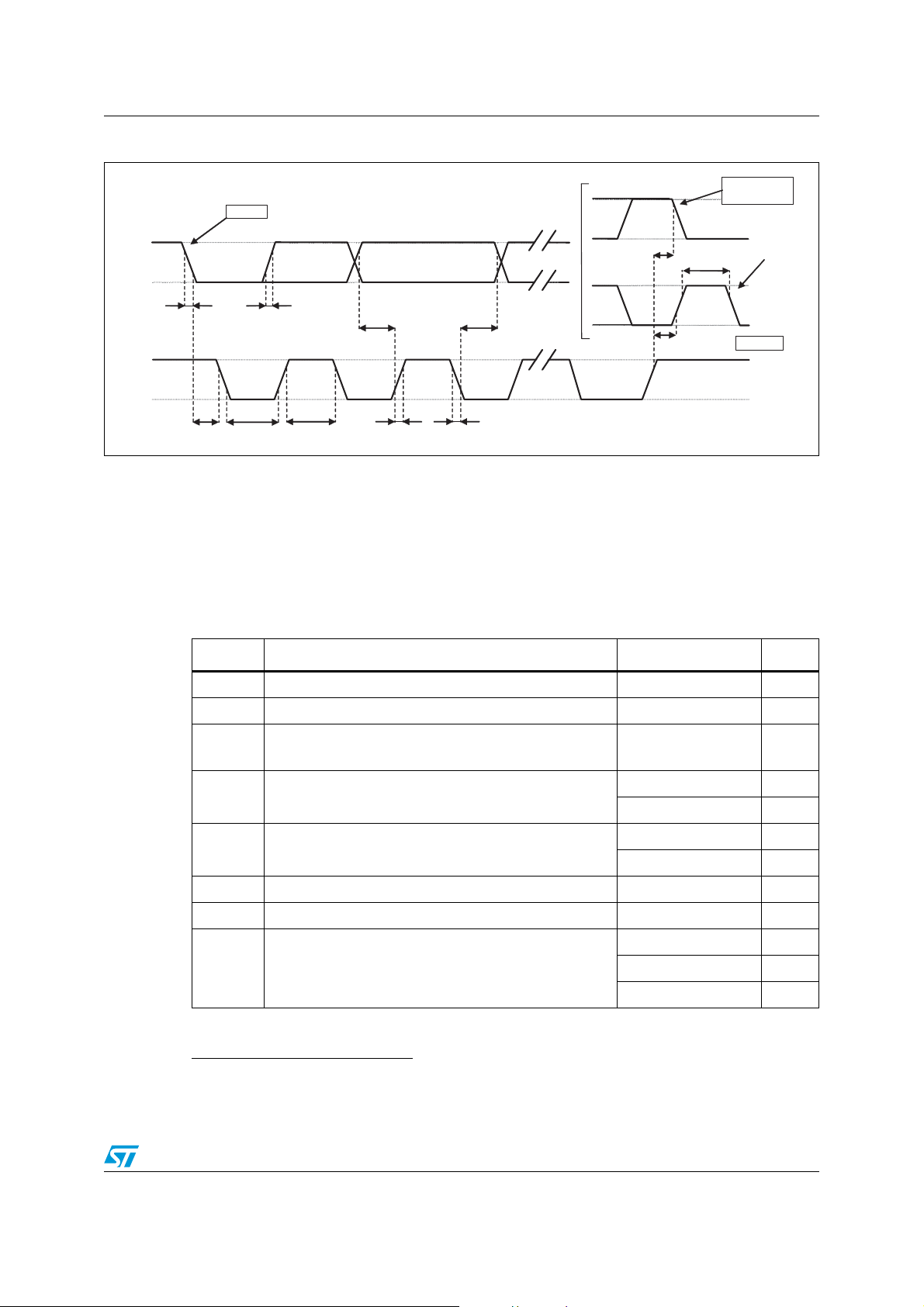
2.3.2 I²C - inter IC control interface
Subject to general operating conditions for Vdd and top.
Table 6. I²C slave timing values
Symbol Parameter
f
(SCL)
t
w(SCLL)
t
w(SCLH)
t
su(SDA)
t
h(SDA)
t
h(ST)
t
su(SR)
t
su(SP)
t
w(SP:SR)
1. Data based on standard I²C protocol requirement, not tested in production.
SCL clock frequency 0 100 0 400 KHz
SCL clock low time 4.7 1.3
SCL clock high time 4.0 0.6
SDA setup time 250 100 ns
SDA data hold time 0.01 3.45 0.01 0.9 µs
START condition hold time 4 0.6
Repeated START condition
setup time
STOP condition setup time 4 0.6
Bus free time between STOP
and START condition
I²C standard mode
Min. Max. Min. Max.
4.7 0.6
4.7 1.3
(1)
I²C fast mode
(1)
Unit
µs
µs
12/43 Doc ID 18160 Rev 3
AIS328DQ Mechanical and electrical specifications
SDA
SCL
t
f(SDA)
t
su(SP)
t
w(SCLL)
t
su(SDA)
t
r(SDA)
t
su(SR)
t
h(ST)
t
w(SCLH)
t
h(SDA)
t
r(SCL)
t
f(SCL)
t
w(SP:SR)
START
REPEATED
START
STOP
STAR
T
Figure 4. I²C slave timing diagram
2.4 Absolute maximum ratings
Stresses above those listed as “absolute maximum ratings” may cause permanent damage
to the device. This is a stress rating only and functional operation of the device under these
conditions is not implied. Exposure to maximum rating conditions for extended periods may
affect device reliability.
Table 7. Absolute maximum ratings
(c)
Symbol Ratings Maximum value Unit
Vdd Supply voltage -0.3 to 4 V
Vdd_IO I/O pin supply voltage -0.3 to 4 V
Input voltage on any control pin
(CS, SCL/SPC, SDA/SDI/SDO, SDO/SA0)
Acceleration (any axis, powered, Vdd = 2.5 V)
(1)
-0.3 to Vdd_IO +0.3 V
3000 g for 0.5 ms
10000 g for 0.1 ms
Acceleration (any axis, unpowered)
(1)
3000 g for 0.5 ms
10000 g for 0.1 ms
Operating temperature range -40 to +105 °C
OP
Storage temperature range -40 to +125 °C
A
A
T
Vin
POW
UNP
T
STG
4 (HBM) kV
ESD Electrostatic discharge protection
1.5 (CDM) kV
200 (MM) V
c. Measurement points are made at 0.2·Vdd_IO and 0.8·Vdd_IO, for both ports.
Doc ID 18160 Rev 3 13/43
 Loading...