

3-axis, low g accelerometer with digital output
Features
■ 3.3 V single supply operation
■ 1.8 V compatible IOs
■ SPI digital output interface
■ 12 bit resolution
■ Interrupt activated by motion
■ Programmable interrupt threshold
■ Embedded self-test
■ High shock survivability
■ ECOPACK
■ Extended temperature range -40 °C to +105 °C
Applications
■ Anti-theft systems and inertial navigation
■ Motion activated functions
■ Vibration monitoring and compensation
■ Tilt measurements
■ Black boxes, event recorders
Description
The AIS326DQ is a three axes digital output
accelerometer that includes a sensing element
and an IC interface able to take the information
from the sensing element and to provide the
measured acceleration signals to the external
world through an SPI serial interface. I
compatible interface is also available.
®
compliant
²
C
AIS326DQ
MEMS inertial sensor
QFPN-28
process developed by ST to produce inertial
sensors and actuators in silicon.
The IC interface instead is manufactured using a
CMOS process that allows high level of
integration to design a dedicated circuit which is
factory trimmed to better match the sensing
element characteristics.
The AIS326DQ has a user selectable full scale of
±2 g, ±6 g and it is capable of measuring
acceleration over a bandwidth of 640 Hz for all
axes. The device bandwidth may be selected
accordingly to the application requirements. The
self-test capability allows the user to check the
functioning of the system.
The device is available in plastic quad flat
package no lead surface mount (QFPN) and it is
specified over a temperature range extending
from -40 °C to +105 °C.
The sensing element, capable of detecting the
acceleration, is manufactured using a dedicated
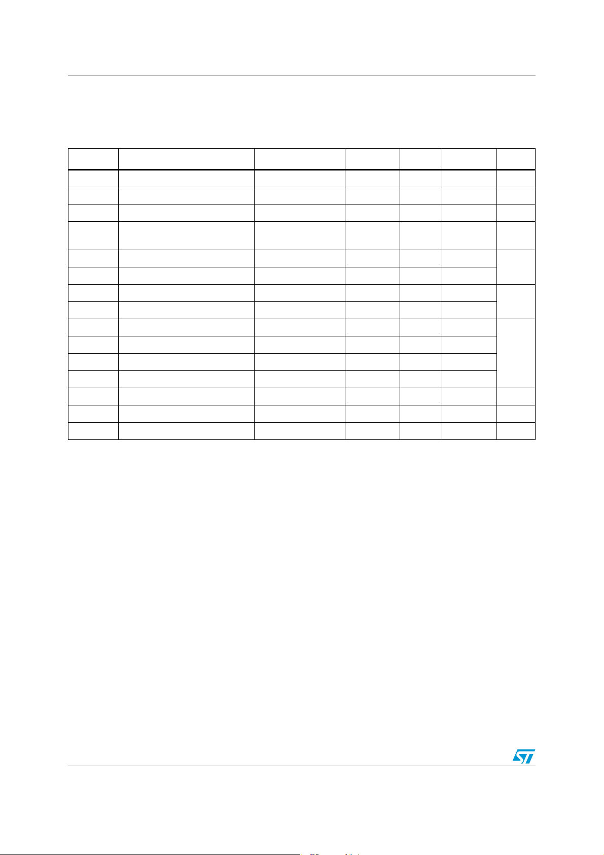
Table 1. Device summary
Order code
AIS326DQ -40 to +105 QFPN-28 Tray
AIS326DQTR -40 to +105 QFPN-28 Tape and reel
June 2010 Doc ID 14956 Rev 4 1/51
Operating temperature
range [° C]
Package Packing
www.st.com
51

Contents AIS326DQ
Contents
1 Block diagram and pin description . . . . . . . . . . . . . . . . . . . . . . . . . . . . . 8
1.1 Block diagram . . . . . . . . . . . . . . . . . . . . . . . . . . . . . . . . . . . . . . . . . . . . . . . 8
1.2 QFPN-28 pin description . . . . . . . . . . . . . . . . . . . . . . . . . . . . . . . . . . . . . . 8
2 Mechanical and electrical specifications . . . . . . . . . . . . . . . . . . . . . . . 10
2.1 Mechanical characteristics . . . . . . . . . . . . . . . . . . . . . . . . . . . . . . . . . . . . 10
2.2 Electrical characteristics . . . . . . . . . . . . . . . . . . . . . . . . . . . . . . . . . . . . . . 12
2.3 Communication interface characteristics . . . . . . . . . . . . . . . . . . . . . . . . . 13
2.3.1 SPI - serial peripheral interface . . . . . . . . . . . . . . . . . . . . . . . . . . . . . . . 13
2.4 Absolute maximum ratings . . . . . . . . . . . . . . . . . . . . . . . . . . . . . . . . . . . . 14
2.5 Terminology . . . . . . . . . . . . . . . . . . . . . . . . . . . . . . . . . . . . . . . . . . . . . . . 15
2.5.1 Sensitivity . . . . . . . . . . . . . . . . . . . . . . . . . . . . . . . . . . . . . . . . . . . . . . . . 15
2.5.2 Zero-g level . . . . . . . . . . . . . . . . . . . . . . . . . . . . . . . . . . . . . . . . . . . . . . 15
2.5.3 Self test . . . . . . . . . . . . . . . . . . . . . . . . . . . . . . . . . . . . . . . . . . . . . . . . . 15
3 Functionality . . . . . . . . . . . . . . . . . . . . . . . . . . . . . . . . . . . . . . . . . . . . . . 16
3.1 Sensing element . . . . . . . . . . . . . . . . . . . . . . . . . . . . . . . . . . . . . . . . . . . . 16
3.2 IC interface . . . . . . . . . . . . . . . . . . . . . . . . . . . . . . . . . . . . . . . . . . . . . . . . 16
3.3 Factory calibration . . . . . . . . . . . . . . . . . . . . . . . . . . . . . . . . . . . . . . . . . . 17
4 Application hints . . . . . . . . . . . . . . . . . . . . . . . . . . . . . . . . . . . . . . . . . . . 18
5 Digital interface . . . . . . . . . . . . . . . . . . . . . . . . . . . . . . . . . . . . . . . . . . . . 19
5.1 SPI bus interface . . . . . . . . . . . . . . . . . . . . . . . . . . . . . . . . . . . . . . . . . . . 19
5.1.1 SPI Read . . . . . . . . . . . . . . . . . . . . . . . . . . . . . . . . . . . . . . . . . . . . . . . . 20
5.1.2 SPI Write . . . . . . . . . . . . . . . . . . . . . . . . . . . . . . . . . . . . . . . . . . . . . . . . 21
5.1.3 SPI Read in 3-wires mode . . . . . . . . . . . . . . . . . . . . . . . . . . . . . . . . . . . 22
6 Register mapping . . . . . . . . . . . . . . . . . . . . . . . . . . . . . . . . . . . . . . . . . . 23
7 Register description . . . . . . . . . . . . . . . . . . . . . . . . . . . . . . . . . . . . . . . . 25
7.1 WHO_AM_I (0Fh) . . . . . . . . . . . . . . . . . . . . . . . . . . . . . . . . . . . . . . . . . . . 25
7.2 OFFSET_X (16h) . . . . . . . . . . . . . . . . . . . . . . . . . . . . . . . . . . . . . . . . . . . 25
2/51 Doc ID 14956 Rev 4

AIS326DQ Contents
7.3 OFFSET_Y (17h) . . . . . . . . . . . . . . . . . . . . . . . . . . . . . . . . . . . . . . . . . . . 25
7.4 OFFSET_Z (18h) . . . . . . . . . . . . . . . . . . . . . . . . . . . . . . . . . . . . . . . . . . . 26
7.5 GAIN_X (19h) . . . . . . . . . . . . . . . . . . . . . . . . . . . . . . . . . . . . . . . . . . . . . . 26
7.6 GAIN_Y (1Ah) . . . . . . . . . . . . . . . . . . . . . . . . . . . . . . . . . . . . . . . . . . . . . 26
7.7 GAIN_Z (1Bh) . . . . . . . . . . . . . . . . . . . . . . . . . . . . . . . . . . . . . . . . . . . . . . 26
7.8 CTRL_REG1 (20h) . . . . . . . . . . . . . . . . . . . . . . . . . . . . . . . . . . . . . . . . . . 27
7.9 CTRL_REG2 (21h) . . . . . . . . . . . . . . . . . . . . . . . . . . . . . . . . . . . . . . . . . . 27
7.10 CTRL_REG3 (22h) . . . . . . . . . . . . . . . . . . . . . . . . . . . . . . . . . . . . . . . . . . 29
7.11 HP_FILTER_RESET (23h) . . . . . . . . . . . . . . . . . . . . . . . . . . . . . . . . . . . . 30
7.12 STATUS_REG (27h) . . . . . . . . . . . . . . . . . . . . . . . . . . . . . . . . . . . . . . . . . 30
7.13 OUTX_L (28h) . . . . . . . . . . . . . . . . . . . . . . . . . . . . . . . . . . . . . . . . . . . . . 30
7.14 OUTX_H (29h) . . . . . . . . . . . . . . . . . . . . . . . . . . . . . . . . . . . . . . . . . . . . . 31
7.15 OUTY_L (2Ah) . . . . . . . . . . . . . . . . . . . . . . . . . . . . . . . . . . . . . . . . . . . . . 31
7.16 OUTY_H (2Bh) . . . . . . . . . . . . . . . . . . . . . . . . . . . . . . . . . . . . . . . . . . . . . 31
7.17 OUTZ_L (2Ch) . . . . . . . . . . . . . . . . . . . . . . . . . . . . . . . . . . . . . . . . . . . . . 32
7.18 OUTZ_H (2Dh) . . . . . . . . . . . . . . . . . . . . . . . . . . . . . . . . . . . . . . . . . . . . . 32
7.19 FF_WU_CFG (30h) . . . . . . . . . . . . . . . . . . . . . . . . . . . . . . . . . . . . . . . . . 33
7.20 FF_WU_SRC (31h) . . . . . . . . . . . . . . . . . . . . . . . . . . . . . . . . . . . . . . . . . 34
7.21 FF_WU_ACK (32h) . . . . . . . . . . . . . . . . . . . . . . . . . . . . . . . . . . . . . . . . . 34
7.22 FF_WU_THS_L (34h) . . . . . . . . . . . . . . . . . . . . . . . . . . . . . . . . . . . . . . . 34
7.23 FF_WU_THS_H (35h) . . . . . . . . . . . . . . . . . . . . . . . . . . . . . . . . . . . . . . . 34
7.24 FF_WU_DURATION (36h) . . . . . . . . . . . . . . . . . . . . . . . . . . . . . . . . . . . . 36
7.25 DD_CFG (38h) . . . . . . . . . . . . . . . . . . . . . . . . . . . . . . . . . . . . . . . . . . . . . 36
7.26 DD_SRC (39h) . . . . . . . . . . . . . . . . . . . . . . . . . . . . . . . . . . . . . . . . . . . . . 37
7.27 DD_ACK (3Ah) . . . . . . . . . . . . . . . . . . . . . . . . . . . . . . . . . . . . . . . . . . . . . 38
7.28 DD_THSI_L (3Ch) . . . . . . . . . . . . . . . . . . . . . . . . . . . . . . . . . . . . . . . . . . 38
7.29 DD_THSI_H (3Dh) . . . . . . . . . . . . . . . . . . . . . . . . . . . . . . . . . . . . . . . . . . 38
7.30 DD_THSE_L (3Eh) . . . . . . . . . . . . . . . . . . . . . . . . . . . . . . . . . . . . . . . . . . 38
7.31 DD_THSE_H (3Fh) . . . . . . . . . . . . . . . . . . . . . . . . . . . . . . . . . . . . . . . . . 38
8 Typical performance characteristics . . . . . . . . . . . . . . . . . . . . . . . . . . . 40
8.1 Mechanical characteristics at 25 °C . . . . . . . . . . . . . . . . . . . . . . . . . . . . . 40
8.2 Mechanical characteristics at -40 °C . . . . . . . . . . . . . . . . . . . . . . . . . . . . 41
Doc ID 14956 Rev 4 3/51

Contents AIS326DQ
8.3 Mechanical characteristics at 105 °C . . . . . . . . . . . . . . . . . . . . . . . . . . . . 42
8.4 Mechanical characteristics derived from measurement in the -40 °C to +105
°C temperature range 43
8.5 Electro-mechanical characteristics at 25 °C . . . . . . . . . . . . . . . . . . . . . . . 44
8.6 Electrical characteristics at 25 °C . . . . . . . . . . . . . . . . . . . . . . . . . . . . . . . 45
8.7 Electrical characteristics at -40 °C . . . . . . . . . . . . . . . . . . . . . . . . . . . . . . 45
8.8 Electrical characteristics at 105 °C . . . . . . . . . . . . . . . . . . . . . . . . . . . . . . 45
9 Soldering information . . . . . . . . . . . . . . . . . . . . . . . . . . . . . . . . . . . . . . . 46
9.1 General guidelines about soldering surface mount accelerometer . . . . . 46
9.2 PCB design guidelines . . . . . . . . . . . . . . . . . . . . . . . . . . . . . . . . . . . . . . . 46
9.2.1 PCB design rules . . . . . . . . . . . . . . . . . . . . . . . . . . . . . . . . . . . . . . . . . . 47
9.3 Stencil design and solder paste application . . . . . . . . . . . . . . . . . . . . . . . 47
9.4 Process consideration . . . . . . . . . . . . . . . . . . . . . . . . . . . . . . . . . . . . . . . 48
10 Package information . . . . . . . . . . . . . . . . . . . . . . . . . . . . . . . . . . . . . . . . 49
11 Revision history . . . . . . . . . . . . . . . . . . . . . . . . . . . . . . . . . . . . . . . . . . . 50
4/51 Doc ID 14956 Rev 4

AIS326DQ List of tables
List of tables
Table 1. Device summary . . . . . . . . . . . . . . . . . . . . . . . . . . . . . . . . . . . . . . . . . . . . . . . . . . . . . . . . . . 1
Table 2. Pin description . . . . . . . . . . . . . . . . . . . . . . . . . . . . . . . . . . . . . . . . . . . . . . . . . . . . . . . . . . . 6
Table 3. Mechanical characteristics @ Vdd = 3.3 V, T = -40 °C to 105 °C unless otherwise noted. . 7
Table 4. Electrical characteristics @ Vdd=3.3 V, T = -40 °C to 105 °C unless otherwise noted . . . . 9
Table 5. SPI slave timing values. . . . . . . . . . . . . . . . . . . . . . . . . . . . . . . . . . . . . . . . . . . . . . . . . . . . 10
Table 6. Absolute maximum ratings . . . . . . . . . . . . . . . . . . . . . . . . . . . . . . . . . . . . . . . . . . . . . . . . . 11
Table 7. Serial interface pin description . . . . . . . . . . . . . . . . . . . . . . . . . . . . . . . . . . . . . . . . . . . . . . 16
Table 8. Registers address map . . . . . . . . . . . . . . . . . . . . . . . . . . . . . . . . . . . . . . . . . . . . . . . . . . . . 20
Table 9. Register . . . . . . . . . . . . . . . . . . . . . . . . . . . . . . . . . . . . . . . . . . . . . . . . . . . . . . . . . . . . . . . 22
Table 10. Register description . . . . . . . . . . . . . . . . . . . . . . . . . . . . . . . . . . . . . . . . . . . . . . . . . . . . . . 22
Table 11. OFFSET_X register . . . . . . . . . . . . . . . . . . . . . . . . . . . . . . . . . . . . . . . . . . . . . . . . . . . . . . 22
Table 12. OFFSET_X register description . . . . . . . . . . . . . . . . . . . . . . . . . . . . . . . . . . . . . . . . . . . . . 22
Table 13. OFFSET_Y register . . . . . . . . . . . . . . . . . . . . . . . . . . . . . . . . . . . . . . . . . . . . . . . . . . . . . . 22
Table 14. OFFSET_Y register description . . . . . . . . . . . . . . . . . . . . . . . . . . . . . . . . . . . . . . . . . . . . . 22
Table 15. OFFSET_Z register . . . . . . . . . . . . . . . . . . . . . . . . . . . . . . . . . . . . . . . . . . . . . . . . . . . . . . 23
Table 16. OFFSET_Z register description . . . . . . . . . . . . . . . . . . . . . . . . . . . . . . . . . . . . . . . . . . . . . 23
Table 17. GAIN_X register . . . . . . . . . . . . . . . . . . . . . . . . . . . . . . . . . . . . . . . . . . . . . . . . . . . . . . . . . 23
Table 18. GAIN_X register description . . . . . . . . . . . . . . . . . . . . . . . . . . . . . . . . . . . . . . . . . . . . . . . . 23
Table 19. GAIN_Y register . . . . . . . . . . . . . . . . . . . . . . . . . . . . . . . . . . . . . . . . . . . . . . . . . . . . . . . . . 23
Table 20. GAIN_Y register description . . . . . . . . . . . . . . . . . . . . . . . . . . . . . . . . . . . . . . . . . . . . . . . . 23
Table 21. GAIN_Z register . . . . . . . . . . . . . . . . . . . . . . . . . . . . . . . . . . . . . . . . . . . . . . . . . . . . . . . . . 23
Table 22. GAIN_Z register description . . . . . . . . . . . . . . . . . . . . . . . . . . . . . . . . . . . . . . . . . . . . . . . . 23
Table 23. CTRL_REG1 register . . . . . . . . . . . . . . . . . . . . . . . . . . . . . . . . . . . . . . . . . . . . . . . . . . . . . 24
Table 24. CTRL_REG1 register description . . . . . . . . . . . . . . . . . . . . . . . . . . . . . . . . . . . . . . . . . . . . 24
Table 25. CTRL_REG2 register . . . . . . . . . . . . . . . . . . . . . . . . . . . . . . . . . . . . . . . . . . . . . . . . . . . . . 24
Table 26. CTRL_REG2 register description . . . . . . . . . . . . . . . . . . . . . . . . . . . . . . . . . . . . . . . . . . . . 25
Table 27. CTRL_REG3 register . . . . . . . . . . . . . . . . . . . . . . . . . . . . . . . . . . . . . . . . . . . . . . . . . . . . . 26
Table 28. CTRL_REG3 register description . . . . . . . . . . . . . . . . . . . . . . . . . . . . . . . . . . . . . . . . . . . . 26
Table 29. STATUS_REG register . . . . . . . . . . . . . . . . . . . . . . . . . . . . . . . . . . . . . . . . . . . . . . . . . . . . 27
Table 30. STATUS_REG register description . . . . . . . . . . . . . . . . . . . . . . . . . . . . . . . . . . . . . . . . . . 27
Table 31. OUTX_L register . . . . . . . . . . . . . . . . . . . . . . . . . . . . . . . . . . . . . . . . . . . . . . . . . . . . . . . . . 27
Table 32. OUTX_L register description . . . . . . . . . . . . . . . . . . . . . . . . . . . . . . . . . . . . . . . . . . . . . . . 27
Table 33. OUTX_H register . . . . . . . . . . . . . . . . . . . . . . . . . . . . . . . . . . . . . . . . . . . . . . . . . . . . . . . . 28
Table 34. OUTX_H register description . . . . . . . . . . . . . . . . . . . . . . . . . . . . . . . . . . . . . . . . . . . . . . . 28
Table 35. OUTY_L register . . . . . . . . . . . . . . . . . . . . . . . . . . . . . . . . . . . . . . . . . . . . . . . . . . . . . . . . . 28
Table 36. OUTY_L register description . . . . . . . . . . . . . . . . . . . . . . . . . . . . . . . . . . . . . . . . . . . . . . . 28
Table 37. OUTY_H register . . . . . . . . . . . . . . . . . . . . . . . . . . . . . . . . . . . . . . . . . . . . . . . . . . . . . . . . 28
Table 38. OUTY_H register description . . . . . . . . . . . . . . . . . . . . . . . . . . . . . . . . . . . . . . . . . . . . . . . 28
Table 39. OUTZ_L register . . . . . . . . . . . . . . . . . . . . . . . . . . . . . . . . . . . . . . . . . . . . . . . . . . . . . . . . . 29
Table 40. OUTZ_L register description. . . . . . . . . . . . . . . . . . . . . . . . . . . . . . . . . . . . . . . . . . . . . . . . 29
Table 41. OUTZ_H register . . . . . . . . . . . . . . . . . . . . . . . . . . . . . . . . . . . . . . . . . . . . . . . . . . . . . . . . 29
Table 42. OUTZ_H register description . . . . . . . . . . . . . . . . . . . . . . . . . . . . . . . . . . . . . . . . . . . . . . . 29
Table 43. FF_WU_CFG register . . . . . . . . . . . . . . . . . . . . . . . . . . . . . . . . . . . . . . . . . . . . . . . . . . . . . 30
Table 44. FF_WU_CFG register description . . . . . . . . . . . . . . . . . . . . . . . . . . . . . . . . . . . . . . . . . . . 30
Table 45. FF_WU_SRC register . . . . . . . . . . . . . . . . . . . . . . . . . . . . . . . . . . . . . . . . . . . . . . . . . . . . . 31
Table 46. FF_WU_SRC register description . . . . . . . . . . . . . . . . . . . . . . . . . . . . . . . . . . . . . . . . . . . 31
Table 47. FF_WU_THS_L register . . . . . . . . . . . . . . . . . . . . . . . . . . . . . . . . . . . . . . . . . . . . . . . . . . . 31
Table 48. FF_WU_THS_L register description. . . . . . . . . . . . . . . . . . . . . . . . . . . . . . . . . . . . . . . . . . 31
Doc ID 14956 Rev 4 5/51

List of tables AIS326DQ
Table 49. FF_WU_THS_H register. . . . . . . . . . . . . . . . . . . . . . . . . . . . . . . . . . . . . . . . . . . . . . . . . . . 31
Table 50. FF_WU_THS_H register description . . . . . . . . . . . . . . . . . . . . . . . . . . . . . . . . . . . . . . . . . 31
Table 51. FF_WU_DURATION register . . . . . . . . . . . . . . . . . . . . . . . . . . . . . . . . . . . . . . . . . . . . . . . 32
Table 52. FF_WU_DURATION register description . . . . . . . . . . . . . . . . . . . . . . . . . . . . . . . . . . . . . . 32
Table 53. DD_CFG register . . . . . . . . . . . . . . . . . . . . . . . . . . . . . . . . . . . . . . . . . . . . . . . . . . . . . . . . 32
Table 54. DD_CFG register description . . . . . . . . . . . . . . . . . . . . . . . . . . . . . . . . . . . . . . . . . . . . . . . 32
Table 55. DD_SRC register . . . . . . . . . . . . . . . . . . . . . . . . . . . . . . . . . . . . . . . . . . . . . . . . . . . . . . . . 33
Table 56. DD_SRC register description . . . . . . . . . . . . . . . . . . . . . . . . . . . . . . . . . . . . . . . . . . . . . . . 33
Table 57. DD_THSI_L register . . . . . . . . . . . . . . . . . . . . . . . . . . . . . . . . . . . . . . . . . . . . . . . . . . . . . . 34
Table 58. DD_THSI_L register description . . . . . . . . . . . . . . . . . . . . . . . . . . . . . . . . . . . . . . . . . . . . . 34
Table 59. DD_THSI_H register . . . . . . . . . . . . . . . . . . . . . . . . . . . . . . . . . . . . . . . . . . . . . . . . . . . . . . 34
Table 60. DD_THSI_H register description . . . . . . . . . . . . . . . . . . . . . . . . . . . . . . . . . . . . . . . . . . . . 34
Table 61. DD_THSE_L register . . . . . . . . . . . . . . . . . . . . . . . . . . . . . . . . . . . . . . . . . . . . . . . . . . . . . 34
Table 62. DD_THSE_L register description . . . . . . . . . . . . . . . . . . . . . . . . . . . . . . . . . . . . . . . . . . . . 34
Table 63. DD_THSE_H register . . . . . . . . . . . . . . . . . . . . . . . . . . . . . . . . . . . . . . . . . . . . . . . . . . . . . 34
Table 64. DD_THSE_H register description . . . . . . . . . . . . . . . . . . . . . . . . . . . . . . . . . . . . . . . . . . . . 35
Table 65. Document revision history . . . . . . . . . . . . . . . . . . . . . . . . . . . . . . . . . . . . . . . . . . . . . . . . . 46
6/51 Doc ID 14956 Rev 4

AIS326DQ List of figures
List of figures
Figure 1. Block diagram . . . . . . . . . . . . . . . . . . . . . . . . . . . . . . . . . . . . . . . . . . . . . . . . . . . . . . . . . . . . 5
Figure 2. Pin connection . . . . . . . . . . . . . . . . . . . . . . . . . . . . . . . . . . . . . . . . . . . . . . . . . . . . . . . . . . . 5
Figure 3. SPI slave timing diagram (2) . . . . . . . . . . . . . . . . . . . . . . . . . . . . . . . . . . . . . . . . . . . . . . . 10
Figure 4. AIS326DQ electrical connection . . . . . . . . . . . . . . . . . . . . . . . . . . . . . . . . . . . . . . . . . . . . . 15
Figure 5. Read and write protocol . . . . . . . . . . . . . . . . . . . . . . . . . . . . . . . . . . . . . . . . . . . . . . . . . . . 16
Figure 6. SPI read protocol . . . . . . . . . . . . . . . . . . . . . . . . . . . . . . . . . . . . . . . . . . . . . . . . . . . . . . . . 17
Figure 7. Multiple bytes SPI read protocol (2 bytes example) . . . . . . . . . . . . . . . . . . . . . . . . . . . . . . 18
Figure 8. SPI Write protocol . . . . . . . . . . . . . . . . . . . . . . . . . . . . . . . . . . . . . . . . . . . . . . . . . . . . . . . . 18
Figure 9. Multiple bytes SPI write protocol (2 bytes example) . . . . . . . . . . . . . . . . . . . . . . . . . . . . . . 18
Figure 10. SPI read protocol in 3-wires mode . . . . . . . . . . . . . . . . . . . . . . . . . . . . . . . . . . . . . . . . . . . 19
Figure 11. X-axis zero-g level at 3.3 V . . . . . . . . . . . . . . . . . . . . . . . . . . . . . . . . . . . . . . . . . . . . . . . . . 36
Figure 12. X-axis sensitivity at 3.3 V . . . . . . . . . . . . . . . . . . . . . . . . . . . . . . . . . . . . . . . . . . . . . . . . . . 36
Figure 13. Y-axis zero-g level at 3.3 V . . . . . . . . . . . . . . . . . . . . . . . . . . . . . . . . . . . . . . . . . . . . . . . . . 36
Figure 14. Y-axis sensitivity at 3.3 V . . . . . . . . . . . . . . . . . . . . . . . . . . . . . . . . . . . . . . . . . . . . . . . . . . 36
Figure 15. Z-axis zero-g level at 3.3 V . . . . . . . . . . . . . . . . . . . . . . . . . . . . . . . . . . . . . . . . . . . . . . . . . 36
Figure 16. Z-axis sensitivity at 3.3 V . . . . . . . . . . . . . . . . . . . . . . . . . . . . . . . . . . . . . . . . . . . . . . . . . . 36
Figure 17. X-axis zero-g level at 3.3 V . . . . . . . . . . . . . . . . . . . . . . . . . . . . . . . . . . . . . . . . . . . . . . . . . 37
Figure 18. X-axis sensitivity at 3.3 V . . . . . . . . . . . . . . . . . . . . . . . . . . . . . . . . . . . . . . . . . . . . . . . . . . 37
Figure 19. Y-axis zero-g level at 3.3 V . . . . . . . . . . . . . . . . . . . . . . . . . . . . . . . . . . . . . . . . . . . . . . . . . 37
Figure 20. Y-axis sensitivity at 3.3 V . . . . . . . . . . . . . . . . . . . . . . . . . . . . . . . . . . . . . . . . . . . . . . . . . . 37
Figure 21. Z-axis zero-g level at 3.3 V . . . . . . . . . . . . . . . . . . . . . . . . . . . . . . . . . . . . . . . . . . . . . . . . . 37
Figure 22. Z-axis sensitivity at 3.3 V . . . . . . . . . . . . . . . . . . . . . . . . . . . . . . . . . . . . . . . . . . . . . . . . . . 37
Figure 23. X-axis zero-g level at 3.3 V . . . . . . . . . . . . . . . . . . . . . . . . . . . . . . . . . . . . . . . . . . . . . . . . . 38
Figure 24. X-axis sensitivity at 3.3 V . . . . . . . . . . . . . . . . . . . . . . . . . . . . . . . . . . . . . . . . . . . . . . . . . . 38
Figure 25. Y-axis zero-g level at 3.3 V . . . . . . . . . . . . . . . . . . . . . . . . . . . . . . . . . . . . . . . . . . . . . . . . . 38
Figure 26. Y-axis sensitivity at 3.3 V . . . . . . . . . . . . . . . . . . . . . . . . . . . . . . . . . . . . . . . . . . . . . . . . . . 38
Figure 27. Z-axis zero-g level at 3.3 V . . . . . . . . . . . . . . . . . . . . . . . . . . . . . . . . . . . . . . . . . . . . . . . . . 38
Figure 28. Z-axis sensitivity at 3.3 V . . . . . . . . . . . . . . . . . . . . . . . . . . . . . . . . . . . . . . . . . . . . . . . . . . 38
Figure 29. X-axis zero-g level change vs. temperature at 3.3 V . . . . . . . . . . . . . . . . . . . . . . . . . . . . . 39
Figure 30. X-axis sensitivity change vs. temperature at 3.3 V . . . . . . . . . . . . . . . . . . . . . . . . . . . . . . . 39
Figure 31. Y-axis zero-g level change vs. temperature at 3.3 V . . . . . . . . . . . . . . . . . . . . . . . . . . . . . 39
Figure 32. Y-axis sensitivity change vs. temperature at 3.3 V . . . . . . . . . . . . . . . . . . . . . . . . . . . . . . . 39
Figure 33. Z-axis zero-g level change vs. temperature at 3.3 V . . . . . . . . . . . . . . . . . . . . . . . . . . . . . 39
Figure 34. Z-axis sensitivity change vs. temperature at 3.3 V . . . . . . . . . . . . . . . . . . . . . . . . . . . . . . . 39
Figure 35. X and Y axes zero-g level as function of supply voltage . . . . . . . . . . . . . . . . . . . . . . . . . . 40
Figure 36. X and Y axes sensitivity as function of supply voltage . . . . . . . . . . . . . . . . . . . . . . . . . . . . 40
Figure 37. Z axis zero-g level as function of supply voltage . . . . . . . . . . . . . . . . . . . . . . . . . . . . . . . . 40
Figure 38. Z axis sensitivity as function of supply voltage . . . . . . . . . . . . . . . . . . . . . . . . . . . . . . . . . . 40
Figure 39. Current consumption in power-down mode (Vdd=3.3 V) . . . . . . . . . . . . . . . . . . . . . . . . . . 41
Figure 40. Current consumption in operational mode (Vdd=3.3 V) . . . . . . . . . . . . . . . . . . . . . . . . . . . 41
Figure 41. Current consumption in power-down mode (Vdd=3.3 V) . . . . . . . . . . . . . . . . . . . . . . . . . . 41
Figure 42. Current consumption in operational mode (Vdd=3.3 V) . . . . . . . . . . . . . . . . . . . . . . . . . . . 41
Figure 43. Current consumption in power-down mode (Vdd=3.3 V) . . . . . . . . . . . . . . . . . . . . . . . . . . 41
Figure 44. Current consumption in operational mode (Vdd=3.3 V) . . . . . . . . . . . . . . . . . . . . . . . . . . . 41
Figure 45. Recommended land and solder mask design for QFPN packages . . . . . . . . . . . . . . . . . . 43
Figure 46. QFPN-28 mechanical data and package dimensions. . . . . . . . . . . . . . . . . . . . . . . . . . . . . 45
Doc ID 14956 Rev 4 7/51
Block diagram and pin description AIS326DQ
1 Block diagram and pin description
1.1 Block diagram
Figure 1. Block diagram
X+
Y+
Z+
a
MUX
Z-
Y-
X-
REFERENCESELF TEST
CHARGE
AMPLIFIER
1.2 QFPN-28 pin description
Figure 2. Pin connection
Z
1
Y
X
DIRECTIONS OF THE
DETECTABLE
ACCELERATIONS
DE
MUX
TRIMMING
CIRCUITS
Reserved
RDY/INT
NC
GND
Vdd
GND
NC
Σ∆
Σ∆
Σ∆
1
Reconstruction
Filter
Reconstruction
Filter
Reconstruction
Filter
CLOCK
NC
NCNCNC
28 22
CONTROL LOGIC
INTERRUPT GEN.
NCNCNC
Regs
Array
&
21
AIS326DQ
(TOP VIEW)
7
814
NC
SDO
SDI/SDO
SPC
Vdd_IO
CS
15
NC
SPI
NC
Reserved
Vdd
Reserved
GND
CK
NC
CS
SPC
SDO/SDI
SDO
RDY/INT
8/51 Doc ID 14956 Rev 4

AIS326DQ Block diagram and pin description
Table 2. Pin description
Pin# Name Function
1 NC Internally not connected
2 GND 0 V supply
3 Vdd Power supply
4 Reserved Either leave unconnected or connect to GND
5 GND 0 V supply
6 RDY/INT Data ready/inertial wake-up and free-fall interrupt
7, 8 NC Internally not connected
9 SDO SPI serial data output
10
11 Vdd_IO Power supply for I/O pads
12 SPC SPI serial port clock
13 CS Chip select (logic 0: SPI enabled, logic 1: SPI disabled)
14, 15 NC Internally not connected
16 CK
17 GND 0 V supply
18 Reserved Either leave unconnected or connect to Vdd_IO
19 Vdd Power supply
20 Reserved Connect to Vdd
21 - 28 NC Internally not connected
SDI/
SDO
SPI serial data input (SDI)
3-wire interface serial data output (SDO)
Optional external clock, if not used either leave unconnected or
connect to GND
Doc ID 14956 Rev 4 9/51
Mechanical and electrical specifications AIS326DQ
2 Mechanical and electrical specifications
2.1 Mechanical characteristics
Table 3. Mechanical characteristics @ Vdd = 3.3 V, T = -40 °C to 105 °C unless otherwise
Symbol Parameter Test conditions Min. Typ.
FS Measurement range
noted
(1)
(3)
FS bit set to 0 ±1.7 ±2.0
(2)
Max. Unit
FS bit set to 1 ±5.3 ±6.0
Full-scale = ±2 g
T = 25 °C, ODR1=40 Hz
Full-scale = ±2 g
T = 25 °C, ODR2=160 Hz
1.0
2.0
Dres Device resolution
Full-scale = ±2 g
T = 25 °C, ODR3 = 640 Hz
Full-scale = ±2 g
T = 25 °C, ODR4 = 2560 Hz
Full-scale = ±2 g
12 bit representation
952 1024 1096
3.9
15.6
So Sensitivity
TCSo
Off
TCOff
Sensitivity change vs
temperature
Zero-g level offset
accuracy
(5),(6)
Zero-g level change vs
temperature
Full-scale = ±6 g
12 bit representation
(4)
Full-scale = ±2 g
12 bit representation
Full-scale = ±2 g
X, Y axis
Full-scale = ±2 g
Z axis
Full-scale = ±6 g
X, Y axis
(4)
Full-scale = ±6 g
(4)
Z axis
Max delta from 25 °C 0.2 mg/
316 340 364
0.025 %/
-100 100
-200 200
-100 100
-200 200
g
mg
LSb/g
°C
mg
°C
Best fit straight line
X, Y axis
Full-scale = ±2 g
ODR = 40 Hz
Best fit straight line
NL Non linearity
(4)
Z axis
Full-scale = ±2 g
ODR = 40 Hz
CrAx Cross axis
(4)
10/51 Doc ID 14956 Rev 4
±2
% FS
±3
-5 5 %
AIS326DQ Mechanical and electrical specifications
Table 3. Mechanical characteristics @ Vdd = 3.3 V, T = -40 °C to 105 °C unless otherwise
Symbol Parameter Test conditions Min. Typ.
V
BW System bandwidth
T
OP
Self-test output change
st
Operating temperature range -40 +105 °C
noted
(1)
(continued)
(9)
(7),(8)
Full-scale= ±2 g
X axis
Y axis
Full-scale= ±2 g
Z axis
Full-scale= ±6 g
X axis
Y axis
Full-scale= ±6 g
Z axis
(2)
Max. Unit
200 460 750
200 460 750
140 360 580
60 160 260
60 160 260
45 120 200
ODRx/4 Hz
Wh Product weight 0.2 gram
1. The product is factory calibrated at 3.3 V. Operation over 3.6 V is not recommended
2. Typical specifications are not guaranteed
3. Verified by wafer level test and specification of initial offset and sensitivity
4. Guaranteed by design
5. Zero-g level offset value after MSL3 preconditioning
6. Offset can be eliminated by enabling the built-in high pass filter (HPF)
7. Self test output changes with the power supply. “Self-test output change” is defined as OUTPUT[LSb]
CTRL_REG1=1)
8. Output data reach 99% of final value after 5/ODR when enabling Self-test mode due to device filtering
9. ODRx is output data rate. Refer to Table 4 for specifications
- OUTPUT[LSb]
(Self-test bit on CTRL_REG1=0)
. 1LSb = 1g/1024 at 12 bit representation, 2 g Full-scale
(Self-test bit on
LSbFull-scale= ±2 g
LSbFull-scale= ±6 g
Doc ID 14956 Rev 4 11/51
Mechanical and electrical specifications AIS326DQ
2.2 Electrical characteristics
Table 4. Electrical characteristics @ Vdd=3.3 V, T = -40 °C to 105 °C unless otherwise noted
Symbol Parameter Test conditions Min. Typ.
Vdd Supply voltage 3.0 3.3 3.6 V
Vdd_IO I/O pads supply voltage
(3)
1.71 Vdd V
Idd Supply current Vdd = 3.3 V 0.67 0.80 mA
IddPdn
VIH Digital high level Input voltage
VIL Digital low level Input voltage
VOH High level output voltage
VOL Low level output voltage
Current consumption
in power-down mode
(3)
(3)
(3)
(3)
0.8*Vdd_IO
0.9*Vdd_IO
ODR1 Output data rate 1 Dec factor = 512 40
ODR2 Output data rate 2 Dec factor = 128 160
ODR3 Output data rate 3 Dec factor = 32 640
ODR4 Output data rate 4 Dec factor = 8 2560
BW System bandwidth
Ton Turn-on time
T
OP
1. The product is factory calibrated at 3.3 V. Operation over 3.6 V is not recommended
2. Typical specifications are not guaranteed
3. Guaranteed by design
4. Digital filter -3 dB frequency
5. Time to obtain valid data after exiting power-down mode
Operating temperature range -40 +105 °C
(4)
(5)
(2)
Max. Unit
220µA
V
0.2*Vdd_IO
V
0.1*Vdd_IO
Hz
ODRx/4 Hz
5/ODRx s
(1)
12/51 Doc ID 14956 Rev 4
AIS326DQ Mechanical and electrical specifications
t
t
t
t
t
t
t
t
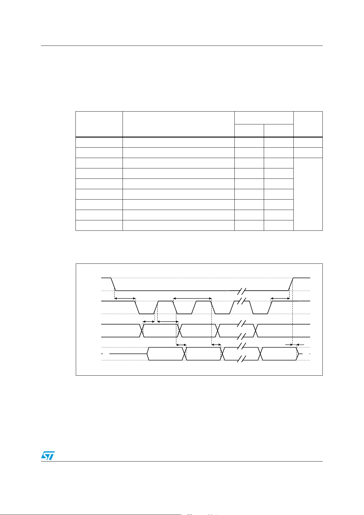
2.3 Communication interface characteristics
2.3.1 SPI - serial peripheral interface
Subject to general operating conditions for Vdd and TOP.
Table 5. SPI slave timing values
(1)
Val ue
Symbol Parameter
Min Max
tc(SPC) SPI clock cycle 125 ns
fc(SPC) SPI clock frequency 8 MHz
tsu(CS) CS setup time 5
th(CS) CS hold time 10
tsu(SI) SDI input setup time 5
Unit
th(SI) SDI input hold time 15
ns
tv(SO) SDO valid output time 55
th(SO) SDO output hold time 7
tdis(SO) SDO output disable time 50
1. Values are guaranteed at 8 MHz clock frequency for SPI with both 4 and 3 wires, based on characterization
results, not tested in production
(2)
h(SI)
v(SO)
(3)
c(SPC)
h(SO)
h(CS)
LSB IN
LSB OUT
(3)
(3)
dis(SO)
(3)
Figure 3. SPI slave timing diagram
CS
(3)
su(CS)
SPC
(3)
su(SI)
SDI
SDO
(3)
(3)
MSB IN
MSB OUT
2. Measurement points are done at 0.2·Vdd_IO and 0.8·Vdd_IO, for both input and output port
3. When no communication is on-going, data on CS, SPC, SDI and SDO are driven by internal pull-up
resistors
Doc ID 14956 Rev 4 13/51
Mechanical and electrical specifications AIS326DQ
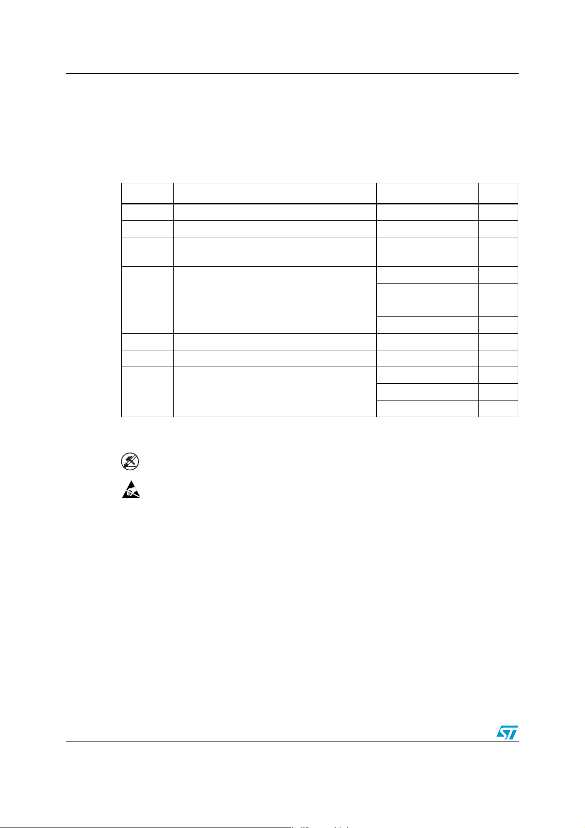
2.4 Absolute maximum ratings
Stresses above those listed as “absolute maximum ratings” may cause permanent damage
to the device. This is a stress rating only and functional operation of the device under these
conditions is not implied. Exposure to maximum rating conditions for extended periods may
affect device reliability.
Table 6. Absolute maximum ratings
Symbol Ratings Maximum value Unit
Vdd Supply voltage
Vdd_IO I/O pins supply voltage
Input voltage on any control pin
(CS, SPC, SDI/SDO, SDO, CK)
Acceleration (any axis, powered, Vdd = 3.3 V)
Acceleration (any axis, unpowered)
Operating temperature range -40 to +105 °C
Storage temperature range -40 to +125 °C
A
A
T
Vin
POW
UNP
T
OP
STG
ESD Electrostatic discharge protection
(1)
(1)
(1)
-0.3 to 6.0 V
-0.3 to Vdd +0.1 V
-0.3 to Vdd_IO +0.3 V
3000 g for 0.5 ms
10000 g for 0.1 ms
3000 g for 0.5 ms
10000 g for 0.1 ms
4.0 (HBM) kV
200 (MM) V
1.5 (CDM) kV
1. Supply voltage on any pin should never exceed 6.0 V.
This is a mechanical shock sensitive device, improper handling can cause permanent
damages to the part.
This is an ESD sensitive device, improper handling can cause permanent damages to
the part.
14/51 Doc ID 14956 Rev 4

AIS326DQ Mechanical and electrical specifications
2.5 Terminology
2.5.1 Sensitivity
Sensitivity describes the gain of the sensor and can be determined e.g. by applying 1 g
acceleration to it. As the sensor can measure DC accelerations this can be done easily by
pointing the axis of interest towards the center of the earth, noting the output value, rotating
the sensor by 180 degrees (point to the sky) and noting the output value again. By doing so,
±1 g acceleration is applied to the sensor. Subtracting the larger output value from the
smaller one, and dividing the result by 2, leads to the actual sensitivity of the sensor. This
value changes very little over temperature and also very little over time. The Sensitivity
tolerance describes the range of sensitivities of a large population of sensors.
2.5.2 Zero-g level
Zero-g level offset (Off) describes the deviation of an actual output signal from the ideal
output signal if there is no acceleration present. A sensor in a steady state on a horizontal
surface will measure 0 g in X axis and 0 g in Y axis whereas the Z axis will measure 1 g. The
output is ideally in the middle of the dynamic range of the sensor (content of OUT registers
00h, 00h with 16 bit representation, data expressed as 2’s complement number). A deviation
from ideal value in this case is called Zero-g offset. Offset is to some extent a result of stress
to a precise MEMS sensor and therefore the offset can slightly change after mounting the
sensor onto a printed circuit board or exposing it to extensive mechanical stress. Offset
changes little over temperature, see “Zero-g level change vs. temperature”. The Zero-g level
of an individual sensor is stable over lifetime. The Zero-g level tolerance describes the range
of Zero-g levels of a population of sensors.
2.5.3 Self test
Self test allows to test the mechanical and electric part of the sensor, allowing the seismic
mass to be moved by means of an electrostatic test-force. The self-test function is off when
the self-test bit of CTRL_REG1 (control register 1) is programmed to ‘0‘. When the self-test
bit of CTRL_REG1 is programmed to ‘1‘an actuation force is applied to the sensor,
simulating a definite input acceleration. In this case the sensor outputs will exhibit a change
in their DC levels which is related to the selected full scale and depending on the Supply
Voltage through the device sensitivity. When Self Test is activated, the device output level is
given by the algebraic sum of the signals produced by the acceleration acting on the sensor
and by the electrostatic test-force. If the output signals change within the amplitude
specified inside Table 3 or 4 then the sensor is working properly and the parameters of the
interface chip are within the defined specification.
Doc ID 14956 Rev 4 15/51

Functionality AIS326DQ
3 Functionality
The AIS326DQ is a high performance, low-power, digital output 3-axes linear accelerometer
packaged in a QFN package. The complete device includes a sensing element and an IC
interface able to take the information from the sensing element and to provide a signal to the
external world through an SPI serial interface.
3.1 Sensing element
A proprietary process is used to create a surface micro-machined accelerometer. The
technology allows to carry out suspended silicon structures which are attached to the
substrate in a few points called anchors and are free to move in the direction of the sensed
acceleration. To be compatible with the traditional packaging techniques a cap is placed on
top of the sensing element to avoid blocking the moving parts during the moulding phase of
the plastic encapsulation.
When an acceleration is applied to the sensor the proof mass displaces from its nominal
position, causing an imbalance in the capacitive half-bridge. This imbalance is measured
using charge integration in response to a voltage pulse applied to the sense capacitor.
At steady state the nominal value of the capacitors are few pF and when an acceleration is
applied the maximum variation of the capacitive load is up to 100 pF.
3.2 IC interface
The complete measurement chain is composed by a low-noise capacitive amplifier which
converts into an analog voltage the capacitive unbalancing of the MEMS sensor and by
three Σ∆ analog-to-digital converters, one for each axis, that translate the produced signal
into a digital bitstream.
The Σ∆ converters are coupled with dedicated reconstruction filters which remove the high
frequency components of the quantization noise and provide low rate and high resolution
digital words.
The charge amplifier and the Σ∆ converters are operated respectively at 61.5 kHz and 20.5
kHz.
The data rate at the output of the reconstruction depends on the user selected decimation
factor (DF) and spans from 40 Hz to 2560 Hz.
The acceleration data may be accessed through an SPI interface thus making the device
particularly suitable for direct interfacing with a microcontroller.
The AIS326DQ features a data-ready signal (RDY) which indicates when a new set of
measured acceleration data is available thus simplifying data synchronization in digital
system employing the device itself.
The AIS326DQ may also be configured to generate an inertial wake-up, direction detection
and free-fall interrupt signal accordingly to a programmed acceleration event along the
enabled axes.
16/51 Doc ID 14956 Rev 4
 Loading...