

ACST6
Overvoltage protected AC switch
Features
■ Triac with overvoltage protection
■ Low I
■ TO-220FPAB insulated package: 1500 V rms
(< 10 mA)
GT
Benefits
■ Enables equipment to meet IEC 61000-4-5
■ High off-state reliability with planar technology
■ Needs no external overvoltage protection
■ Reduces the power passive component count
■ High immunity against fast transients
described in IEC 61000-4-4 standards
Applications
■ AC mains static switching in appliance and
industrial control systems
■ Drive of medium power AC loads such as:
– Universal motor of washing machine drum
– Compressor for fridge or air conditioner
OUT
G
OUT
COM
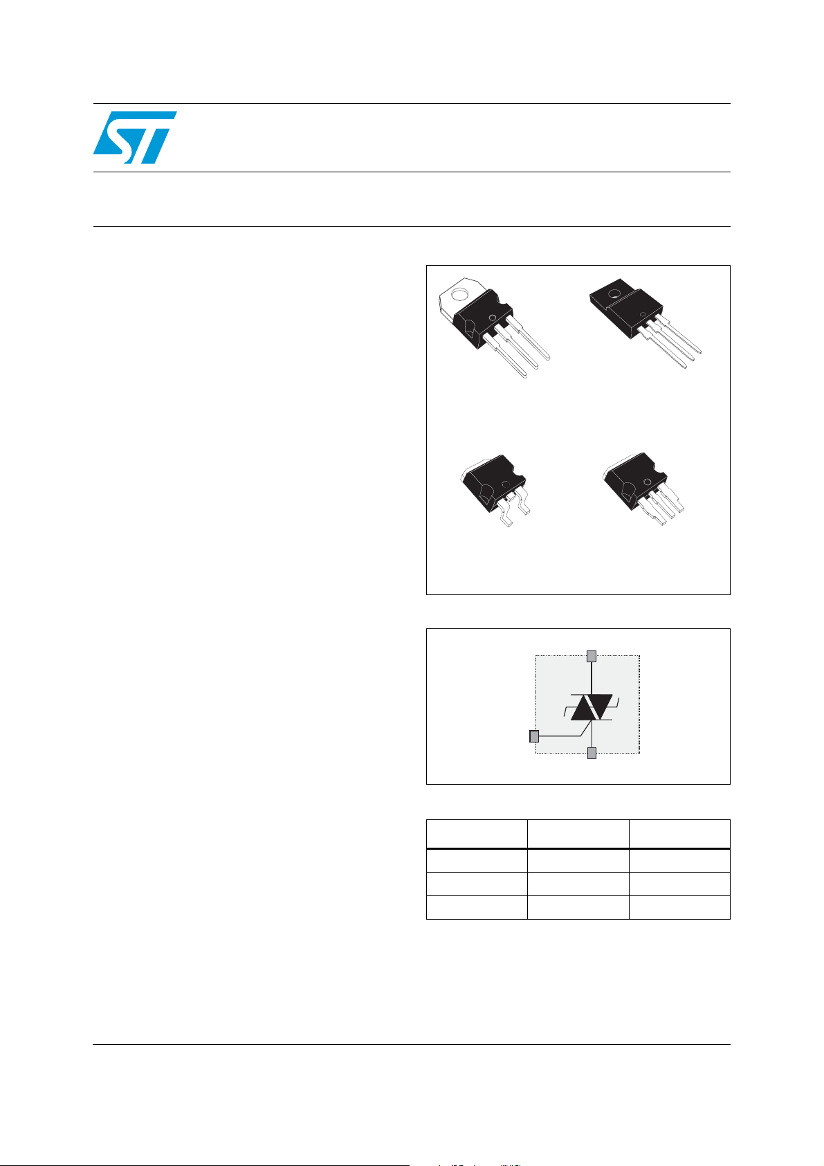
TO-220AB
ACST610-8T
OUT
G
COM
TO-220FPAB
ACST610-8FP
OUT
D²PAK
ACST610-8G
ACST610-8R
Figure 1. Functional diagram
OUT
G
OUT
COM
G
OUT
COM
I²PAK
Description
The ACST6 series belongs to the ACS™/ACST
power switch family built with A.S.D.
specific discrete) technology. This high
performance device is suited to home appliances
or industrial systems, and drives loads up to 6 A.
This ACST6 switch embeds a Triac structure and
a high voltage clamping device able to absorb the
inductive turn-off energy and withstand line
transients such as those described in the
IEC 61000-4-5 standards. The ACST610 needs
only low gate current to be activated
(I
< 10 mA) and still shows a high noise
GT
immunity complying with IEC standards such as
IEC 61000-4-4 (fast transient burst test).
July 2010 Doc ID 7297 Rev 10 1/15
®
(application
G
COM
Table 1. Device summary
Symbol Value Unit
I
T(RMS)
V
DRM/VRRM
I
GT
6A
800 V
10 mA
TM: ACS is a trademark of STMicroelectronics.
®: A.S.D. is a registered trademark of
STMicroelectronics
www.st.com
15
Characteristics ACST6
1 Characteristics
Table 2. Absolute ratings (limiting values)
Symbol Parameter Value Unit
TO-220FPAB T
TO-220AB/
2
I
T(RMS)
I
TSM
I
dI/dt
V
P
G(AV)
P
I
GM
T
V
INS(RMS)
On-state rms current (full sine wave)
Non repetitive surge peak on-state current Tj
initial = 25 °C, ( full cycle sine wave)
2
tI2t for fuse selection tp = 10 ms 13 A2s
Critical rate of rise on-state current
= 2 x I
I
G
Non repetitive line peak pulse voltage
PP
GT, (tr
≤ 100 ns)
(1)
Average gate power dissipation Tj = 125 °C 0.1 W
Peak gate power dissipation (tp = 20 µs) Tj = 125 °C 10 W
GM
Peak gate current (tp = 20 µs) Tj = 125 °C 1.6 A
Storage temperature range -40 to +150 °C
stg
T
Operating junction temperature range -40 to +125 °C
j
Maximum lead solder temperature during 10 ms (at 3 mm from plastic case) 260 °C
T
l
Insulation rms voltage
1. According to test described in IEC 61000-4-5 standard and Figure 19.
Table 3. Electrical characteristics
D
PA K / I2PA K
D2PA K w i t h
2
copper
1cm
F = 60 Hz t
F = 50 Hz t
F = 120 Hz T
TO-220FPAB
= 92 °C
c
6
= 106 °C
T
c
= 62 °C 1.5
T
amb
= 16.7 ms 47 A
p
= 20 ms 45 A
p
= 125 °C 100 A/µs
j
Tj = 25 °C 2 kV
1500 V
A
Symbol Test conditions Quadrant T
(1)
I
GT
V
V
I
H
dV/dt
(dI/dt)
V
1. Minimum IGT is guaranteed at 5% of IGT max
V
= 12 V, RL = 33 Ω I - II - III 25 °C MAX. 10 mA
OUT
V
= 12 V, RL = 33 Ω I - II - III 25 °C MAX. 1.0 V
GT
GD
I
I
CL
(2)
L
L
OUT
V
= V
OUT
I
= 500 mA 25 °C MAX. 25 mA
OUT
I
= 1.2 x I
G
I
= 1.2 x I
G
(2)
V
OUT
(2)
(dV/dt)c = 15 V/µs 125 °C MIN. 3.5 A/ms
c
I
= 0.1 mA, t
CL
, RL = 3.3 kΩ I - II - III 125 °C MIN. 0.2 V
DRM
GT
GT
= 67 % V
, gate open 125 °C MIN. 500 V/µs
DRM
= 1 ms 25 °C MIN. 850 V
p
2. For both polarities of OUT pin referenced to COM pin
2/15 Doc ID 7297 Rev 10
j
Val ue Unit
I - III 25 °C MAX. 30 mA
II 25 °C MAX. 40 mA
ACST6 Characteristics
Table 4. Static characteristics
Symbol Test conditions Value Unit
I
= 2.1 A, t
OUT
(1)
V
V
R
I
I
TM
T0
(1)
d
DRM
RRM
(1)
= 8.5 A, t
I
OUT
Threshold voltage Tj = 125 °C MAX. 0.9 V
Dynamic resistance Tj = 125 °C MAX. 80 mΩ
V
= V
OUT
1. For both polarities of OUT pin referenced to COM pin
Table 5. Thermal resistances
Symbol Parameter Value Unit
= 500 µs
p
= 500 µs 1.7
p
Tj = 25 °C MAX.
Tj = 25 °C MAX. 20 µA
/ V
DRM
RRM
= 125 °C MAX. 500 µA
T
j
1.4
V
Rt
h(j-a)
2
copper pad) D2PA K 4 5
R
Junction to ambient (soldered on 1 cm
Junction to case for full cycle sine wave conduction
th(j-c)
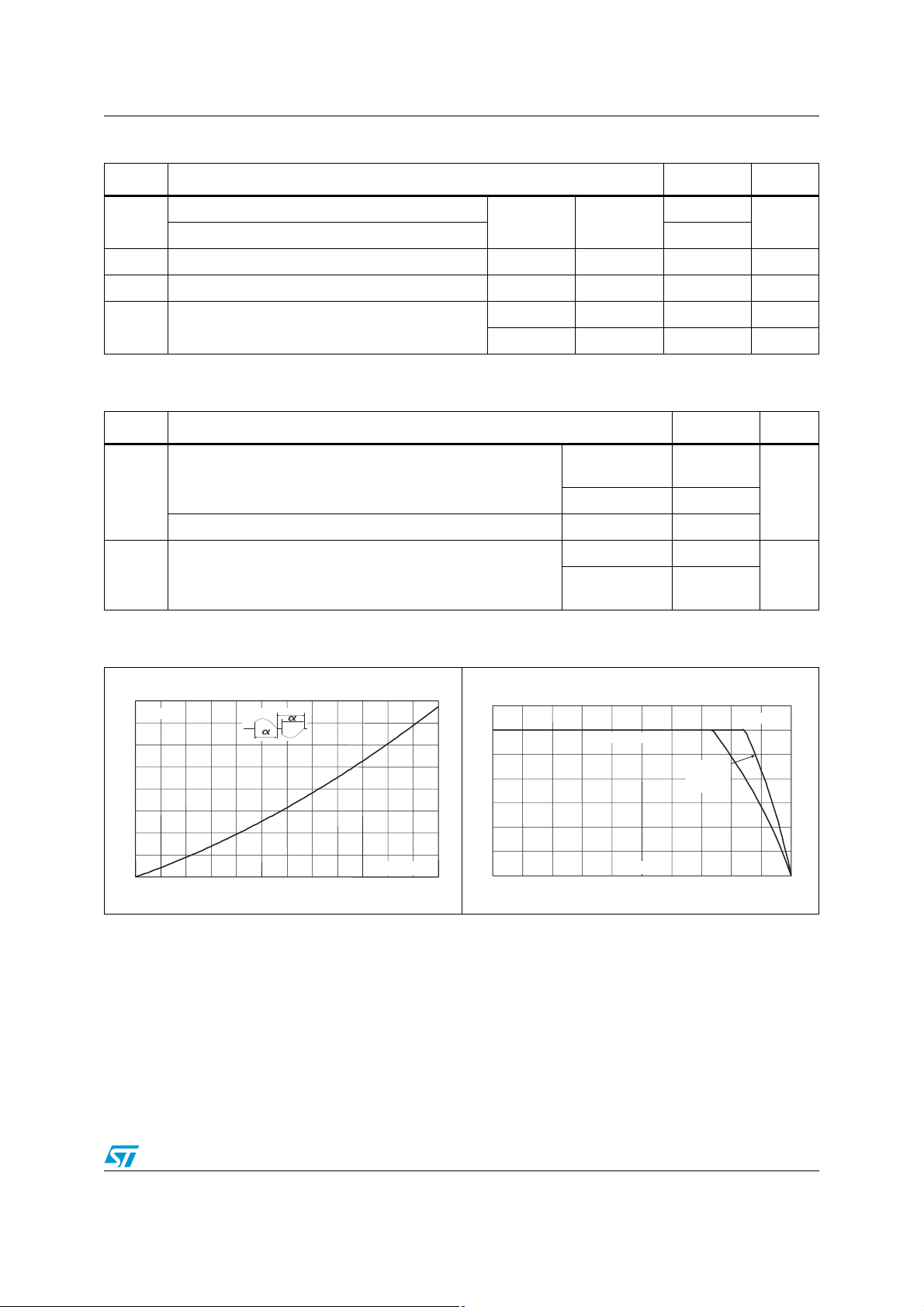
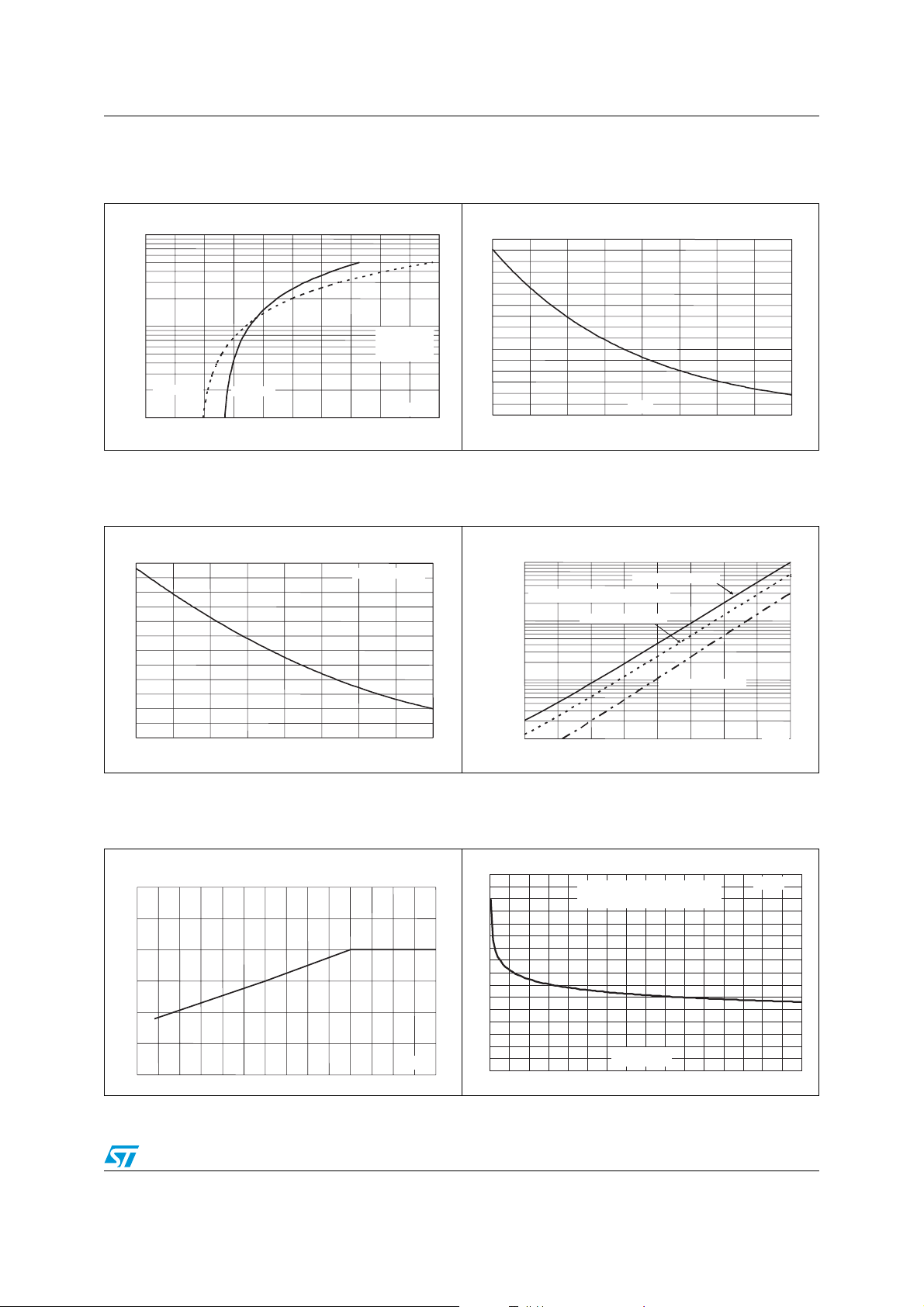
Figure 2. Maximum power dissipation versus
rms on-state current
P(W)
Junction to ambient
8
α = 180°
7
6
5
4
3
2
1
0
0123456
180°
I
(A)
T(RMS)
TO-220AB
TO-220FPAB
2
PAK 65
I
60
°C/W
TO-220FPAB 4.25
TO-220AB
2
D
PA K , I2PA K
2.5
°C/W
Figure 3. On-state rms current versus case
temperature (full cycle)
I
(A)
T(RMS)
7
6
5
4
3
2
1
0
0 25 50 75 100 125
TO-220FPAB
TC(°C)
TO-220AB
D²PAK
I²PAK
α
= 180°
Doc ID 7297 Rev 10 3/15
Characteristics ACST6
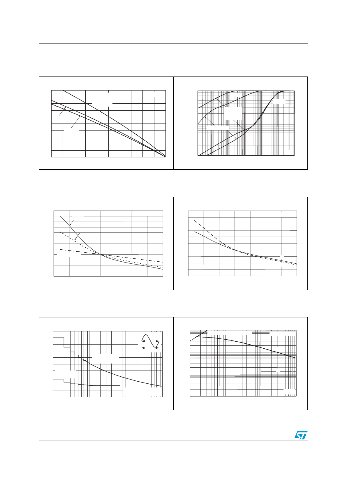
Figure 4. On-state rms current versus
ambient temperature
Figure 5. Relative variation of thermal
impedance versus pulse duration
(free air convection, full cycle)
I
(A)
T(RMS)
2.5
2.0
1.5
TO-220FPAB
TO220AB
1.0
0.5
0.0
0 25 50 75 100 125
I2PAK
D2PAK with
copper
surface = 1
2
cm
Ta(°C)
α=180°
Figure 6. Relative variation of gate trigger
current (I
) and voltage (VGT)
GT
versus junction temperature
Figure 7. Relative variation of holding
K = [Zth/ Rth]
1.0E+00
Z
th(j-c)
Z
TO-220AB
D²PAK
1.0E-01
I²PAK
TO-220FPAB
1.0E-02
1.0E-03 1.0E-01 1.0E+01 1.0E+03
current (IH) and latching current (IL)
versus junction temperature
th(j-a)
tp(s)
IGT,VGT[Tj] / IGT,VGT[Tj= 25 °C]
3.0
2.5
2.0
1.5
1.0
0.5
0.0
-50 -25 0 25 50 75 100 125
IGTQ3
V Q1-Q2-Q3
GT
IGTQ1-Q2
Figure 8. Surge peak on-state current
versus number of cycles
I
(A)
TSM
50
40
30
20
Repetitive
TC=106 °C
10
0
1 10 100 1000
Non repetitive
Tjinitial = 25 °C
(typical values)
t = 20 ms
One cycle
Number of cycles
Number of cycles
Tj(°C)
IH,IL[Tj] / IH,IL[Tj= 25 °C]
2.5
2.0
1.5
1.0
0.5
0.0
-50 -25 0 25 50 75 100 125
Tj(°C)
(typical values)
I
L
I
H
Figure 9. Non repetitive surge peak on-state
current and corresponding value of
2
I
t versus sinusoidal pulse width
I
(A), I²t (A²s)
TSM
1000
100
10
1
0.01 0.10 1.00 10.00
dl /dt limitation: 100 A / µs
Tjinitial = 25 °C
I
TSM
I²t
tp(ms)
4/15 Doc ID 7297 Rev 10
ACST6 Characteristics
Figure 10. On-state characteristics
(maximum values)
ITM(A)
100
10
Tj= 125 °C
1
012345
Tj= 25 °C
Tjmax:
Vto= 0.90 V
Rd= 80 m
VTM(V)
Ω
Figure 12. Relative variation of static dV/dt
immunity versus junction
temperature (gate open)
dV/dt [Tj] / dV/dt [Tj= 125 °C]
6
5
4
VD=VR= 536 V
Figure 11. Relative variation of critical rate of
decrease of main current (dI/dt)
c
versus junction temperature
(dl/dt)c[Tj] / (dl/dt)c[Tj= 125 °C]
8
7
6
5
4
3
2
1
0
25 50 75 100 125
Tj(°C)
Figure 13. Relative variation of leakage
current versus junction
temperature
I
DRM/IRRM[Tj;VDRM/VRRM
1.0E+00
Different blocking voltages
1.0E-01
V
DRM=VRRM
] / I
DRM/IRRM[Tj
V
DRM=VRRM
= 600 V
= 125 °C; 800 V]
= 800V
3
2
1
0
25 50 75 100 125
Figure 14. Relative variation of clamping
voltage (V
) versus junction
CL
temperature (minimum values)
V[Tj] / V [Tj= 25 °C]
CL CL
1.15
1.10
1.05
1.00
0.95
0.90
0.85
-50 -25 0 25 50 75 100 125
Tj(°C)
Tj(°C)
1.0E-02
1.0E-03
25 50 75 100 125
V
DRM=VRRM
= 200 V
Tj(°C)
Figure 15. Thermal resistance junction to
ambient versus copper surface
under tab
Rth(j-a)(°C/W)
80
70
60
50
40
30
20
10
0
0 5 10 15 20 25 30 35 40
Printed circuit board FR4,
copper thickness = 35 µm
SCU(cm²)
D²PAK
Doc ID 7297 Rev 10 5/15
Application information ACST6
2 Application information
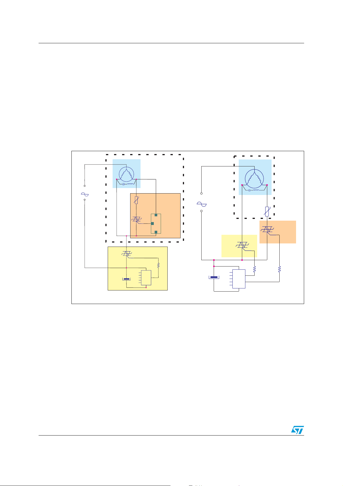
2.1 Typical application description
The ACST6 device has been designed to control medium power load, such as AC motors in
home appliances. Thanks to its thermal and turn off commutation performances, the ACST6
switch is able to drive an inductive load up to 6 A with no turn off additional snubber. It also
provides high thermal performances in static and transient modes such as the compressor
inrush current or high torque operating conditions of an AC motor. Thanks to its low gate
triggering current level, the ACST6 can be driven directly by an MCU through a simple gate
resistor as shown Figure 16 and Figure 17.
Figure 16. Compressor control – typical diagram
Compressor
AC Mains
PTC
ACST
ACST
Power supply
Compressor with integrated e-starter
Electronic
thermostat
Gate
Driver
2
1
3
Rg
Electronic
starter
logical circuitry
Compressor
AC Mains
PTC
ACST
Run
ACST
switch
Rg
Gate
Power supply
Driver
Compressor with external electronic drive
Start
switch
Rg
6/15 Doc ID 7297 Rev 10

ACST6 Application information
Figure 17. Universal drum motor control – typical diagram
Universal motor
Stator
AC Mains
Speed motor
Rotor
ACST
regulation
Vcc
2.2 AC line transient voltage ruggedness
12V
Motor direction
setting
MCU
Rg
MCU
In comparison with standard Triacs, which are not robust against surge voltage, the ACST6
is self-protected against over-voltage, specified by the new parameter V
. The ACST6
CL
switch can safely withstand AC line transient voltages either by clamping the low energy
spikes, such as inductive spikes at switch off, or by switching to the on state (for less than 10
ms) to dissipate higher energy shocks through the load. This safety feature works even with
high turn-on current ramp up.
The test circuit of Figure 18 represents the ACST6 application, and is used to stress the
ACST switch according to the IEC 61000-4-5 standard conditions. With the additional effect
of the load which is limiting the current, the ACST switch withstands the voltage spikes up to
2 kV on top of the peak line voltage. The protection is based on an overvoltage crowbar
technology. The ACST6 folds back safely to the on state as shown in Figure 19. The ACST6
recovers its blocking voltage capability after the surge and the next zero current crossing.
Such a non repetitive test can be done at least 10 times on each AC line voltage polarity.
Doc ID 7297 Rev 10 7/15

Application information ACST6
Figure 18. Overvoltage ruggedness test circuit for resistive and inductive loads for
IEC 61000-4-5 standards
R = 18 , L = 2 µH, Vsurge = 2 kV
Rg = 220ΩΩ
Surge generator
2kV surge
Rgene
Filtering unit
Model of the load
R
L
AC Mains
Figure 19. Typical current and voltage waveforms across the ACST6 during
IEC 61000-4-5 standard test
V
peak=VCL
1.2/50 µs voltage surge
V
0
ACST6
Rg
I
= 120 A
peak
I
8/15 Doc ID 7297 Rev 10
8/20 µs current surge
0
dI/dt = 150 A/µs

ACST6 Ordering information scheme
3 Ordering information scheme
Figure 20. Ordering information scheme
ACS T 6 10 - 8 G TR
AC switch
Topology
T = Triac
On-state rms current
6 = 6 A
Triggering gate current
10 = 10 mA
Repetitive peak off-state voltage
8 = 800 V
Package
FP = TO-220FPAB
T = TO-220AB
R = I²PAK
G = D²PAK
Delivery mode
TR = Tape and reel
Blank = Tube
Doc ID 7297 Rev 10 9/15

Package information ACST6
4 Package information
● Epoxy meets UL94, V0
● Cooling method: by conduction (C)
● Recommended torque value (TO220AB, TO220FPAB): 0.4 to 0.6 N·m
In order to meet environmental requirements, ST offers these devices in different grades of
ECOPACK
specifications, grade definitions and product status are available at: www.st.com
ECOPACK
Table 6. TO-220AB dimensions
®
packages, depending on their level of environmental compliance. ECOPACK®
®
is an ST trademark.
.
Dimensions
Ref.
Millimeters Inches
Min. Max. Min. Max.
A 4.40 4.60 0.173 0.181
C 1.23 1.32 0.048 0.051
H2
Dia
A
C
D 2.40 2.72 0.094 0.107
E 0.49 0.70 0.019 0.027
L2
F2
F1
L5
L6
L9
L4
F
G1
L7
F 0.61 0.88 0.024 0.034
F1 1.14 1.70 0.044 0.066
F2 1.14 1.70 0.044 0.066
G 4.95 5.15 0.194 0.202
D
G1 2.40 2.70 0.094 0.106
H2 10 10.40 0.393 0.409
L2 16.4 typ. 0.645 typ.
M
E
L4 13 14 0.511 0.551
L5 2.65 2.95 0.104 0.116
G
L6 15.25 15.75 0.600 0.620
L7 6.20 6.60 0.244 0.259
L9 3.50 3.93 0.137 0.154
10/15 Doc ID 7297 Rev 10
M 2.6 typ. 0.102 typ.
Diam. 3.75 3.85 0.147 0.151

ACST6 Package information
Table 7. TO-220FPAB dimensions
Dimensions
Ref.
Millimeters Inches
Min. Max. Min. Max.
A 4.4 4.6 0.173 0.181
A
H
B
B 2.5 2.7 0.098 0.106
D 2.5 2.75 0.098 0.108
E 0.45 0.70 0.018 0.027
Dia
L6
L2
L3
L5
F1
L4
F2
F
G1
G
D
L7
E
F 0.75 1 0.030 0.039
F1 1.15 1.70 0.045 0.067
F2 1.15 1.70 0.045 0.067
G 4.95 5.20 0.195 0.205
G1 2.4 2.7 0.094 0.106
H 10 10.4 0.393 0.409
L2 16 Typ. 0.63 Typ.
L3 28.6 30.6 1.126 1.205
L4 9.8 10.6 0.386 0.417
L5 2.9 3.6 0.114 0.142
L6 15.9 16.4 0.626 0.646
L7 9.00 9.30 0.354 0.366
Dia. 3.00 3.20 0.118 0.126
Doc ID 7297 Rev 10 11/15

Package information ACST6
Table 8. D
L2
L
L3
2
PAK dimensions
E
A1
B2
B
G
* FLAT ZONE NO LESSTHAN 2mm
Dimensions
Ref.
Millimeters Inches
Min. Max. Min. Max.
A 4.40 4.60 0.173 0.181
A
A1 2.49 2.69 0.098 0.106
C2
A2 0.03 0.23 0.001 0.009
B 0.70 0.93 0.027 0.037
D
B2 1.14 1.70 0.045 0.067
C 0.45 0.60 0.017 0.024
C2 1.23 1.36 0.048 0.054
C
R
D 8.95 9.35 0.352 0.368
E 10.00 10.40 0.393 0.409
A2
G 4.88 5.28 0.192 0.208
L 15.00 15.85 0.590 0.624
M
*
V2
L2 1.27 1.40 0.050 0.055
L3 1.40 1.75 0.055 0.069
M 2.40 3.20 0.094 0.126
R 0.40 typ. 0.016 typ.
V2 0° 8° 0° 8°
Figure 21. Footprint (dimensions in mm)
16.90
10.30
8.90
3.70
5.08
1.30
12/15 Doc ID 7297 Rev 10

ACST6 Package information
Table 9. I2PAK double track dimensions
Dimensions
Ref.
Millimeters Inches
Min. Max. Min. Max.
A
E
L2
L3
L
Cropping
direction
C2
D
A 4.40 4.60 0.173 0.181
A1 2.49 2.69 0.098 0.106
B 0.70 0.93 0.027 0.037
B2 1.14 1.70 0.045 0.067
C 0.45 0.60 0.018 0.024
C2 1.23 1.36 0.048 0.053
A1
G
B2
B
C
D 8.95 9.35 0.352 0.368
E 10 10.40 0.394 0.409
G 4.88 5.28 0.192 0.208
L 16.70 17.5 0.657 0.689
L2 1.27 1.40 0.050 0.055
L3 13.82 14.42 0.544 0.568
Doc ID 7297 Rev 10 13/15

Ordering information ACST6
5 Ordering information
Table 10. Ordering information
Order code Marking Package Weight Base Qty Packing mode
ACST610-8FP
ACST610-8G D2PAK 1.5 g 50 Tube
ACST610-8GTR D
ACST6108
ACST610-8R I
ACST610-8T TO-220AB 1.5 g 50 Tube
6 Revision history
Table 11. Document revision history
Date Revision Changes
Jan-2002 7F Previous issue.
09-May-2005 8 Layout update. No content change.
18-Dec-2009 9
01-Jul-2010 10 Updated Figure 20.
TO-220FPAB 2.4 g 50 Tube
2
PAK 1.5 g 1000 Tape and reel
2
PAK 2.3 g 50 Tube
Document structure and parameter presentation revised for
consistency with other ACST documents. No technical changes.
Order codes updated.
14/15 Doc ID 7297 Rev 10

ACST6
Please Read Carefully:
Information in this document is provided solely in connection with ST products. STMicroelectronics NV and its subsidiaries (“ST”) reserve the
right to make changes, corrections, modifications or improvements, to this document, and the products and services described herein at any
time, without notice.
All ST products are sold pursuant to ST’s terms and conditions of sale.
Purchasers are solely responsible for the choice, selection and use of the ST products and services described herein, and ST assumes no
liability whatsoever relating to the choice, selection or use of the ST products and services described herein.
No license, express or implied, by estoppel or otherwise, to any intellectual property rights is granted under this document. If any part of this
document refers to any third party products or services it shall not be deemed a license grant by ST for the use of such third party products
or services, or any intellectual property contained therein or considered as a warranty covering the use in any manner whatsoever of such
third party products or services or any intellectual property contained therein.
UNLESS OTHERWISE SET FORTH IN ST’S TERMS AND CONDITIONS OF SALE ST DISCLAIMS ANY EXPRESS OR IMPLIED
WARRANTY WITH RESPECT TO THE USE AND/OR SALE OF ST PRODUCTS INCLUDING WITHOUT LIMITATION IMPLIED
WARRANTIES OF MERCHANTABILITY, FITNESS FOR A PARTICULAR PURPOSE (AND THEIR EQUIVALENTS UNDER THE LAWS
OF ANY JURISDICTION), OR INFRINGEMENT OF ANY PATENT, COPYRIGHT OR OTHER INTELLECTUAL PROPERTY RIGHT.
UNLESS EXPRESSLY APPROVED IN WRITING BY AN AUTHORIZED ST REPRESENTATIVE, ST PRODUCTS ARE NOT
RECOMMENDED, AUTHORIZED OR WARRANTED FOR USE IN MILITARY, AIR CRAFT, SPACE, LIFE SAVING, OR LIFE SUSTAINING
APPLICATIONS, NOR IN PRODUCTS OR SYSTEMS WHERE FAILURE OR MALFUNCTION MAY RESULT IN PERSONAL INJURY,
DEATH, OR SEVERE PROPERTY OR ENVIRONMENTAL DAMAGE. ST PRODUCTS WHICH ARE NOT SPECIFIED AS "AUTOMOTIVE
GRADE" MAY ONLY BE USED IN AUTOMOTIVE APPLICATIONS AT USER’S OWN RISK.
Resale of ST products with provisions different from the statements and/or technical features set forth in this document shall immediately void
any warranty granted by ST for the ST product or service described herein and shall not create or extend in any manner whatsoever, any
liability of ST.
ST and the ST logo are trademarks or registered trademarks of ST in various countries.
Information in this document supersedes and replaces all information previously supplied.
The ST logo is a registered trademark of STMicroelectronics. All other names are the property of their respective owners.
© 2010 STMicroelectronics - All rights reserved
Australia - Belgium - Brazil - Canada - China - Czech Republic - Finland - France - Germany - Hong Kong - India - Israel - Italy - Japan -
STMicroelectronics group of companies
Malaysia - Malta - Morocco - Philippines - Singapore - Spain - Sweden - Switzerland - United Kingdom - United States of America
www.st.com
Doc ID 7297 Rev 10 15/15
 Loading...