

Features
■ Triac with overvoltage crowbar technology
■ Low I
(I
■ High noise immunity: static dV/dt > 2000 V/µs
Benefits
■ Enables equipment to meet IEC 61000-4-5
■ High off-state reliability with planar technology
■ Need no external over voltage protection
■ Reduces the power passive component count
■ High immunity against fast transients
described in IEC 61000-4-4 standards
(<10 mA) or high immunity
GT
<35 mA) version
GT
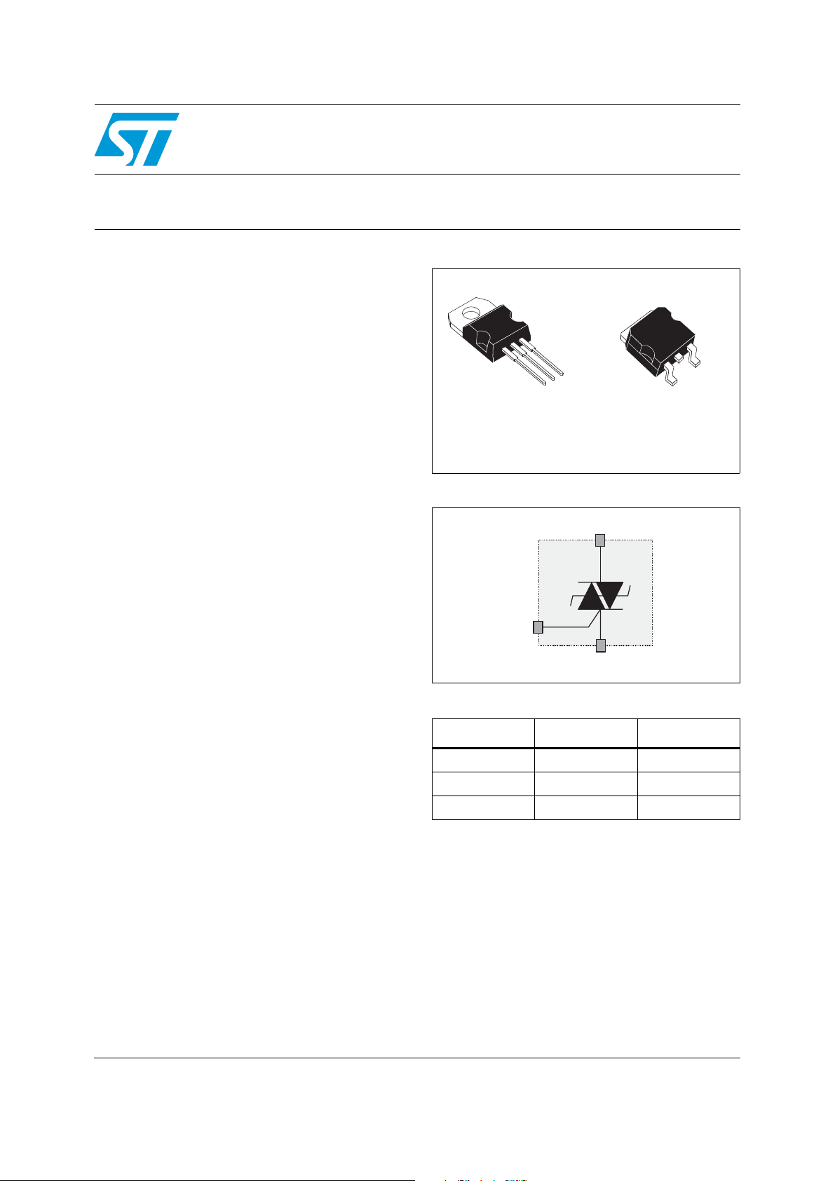
ACST12
Overvoltage protected AC switch
OUT
G
OUT
COM
TO-220AB
ACST1210-7T
ACST1235-7T
Figure 1. Functional diagram
OUT
G
COM
D2PA K
ACST1210-7G
ACST1235-7G
OUT
Applications
■ AC mains static switching in appliance and
industrial control systems
■ Drive of medium power AC loads such as:
– Universal motor of washing machine drum
– Compressor for fridge or air conditioner
Description
The ACST12 series belongs to the ACS™/ACST
power switch family built with A.S.D.
specific discrete) technology. This high
performance device is suited to home appliances
or industrial systems and drives loads up to 12 A.
This ACST12 switch embeds a Triac structure and
a high voltage clamping device able to absorb the
inductive turn-off energy and withstand line
transients such as those described in the
IEC 61000-4-5 standard. The ACST1210-7 needs
a low gate current to be activated (I
and still provides a high electrical noise immunity
complying with the IEC 61000-4-4 standard. The
ACST1235-7 offers an extremely high static dV/dt
immunity of 2 kV/µs minimum.
®
(application
< 10 mA)
GT
G
COM
Table 1. Device summary
Symbol Value Unit
I
T(RMS)
V
DRM/VRRM
I
GT
TM: ACS is a trademark of STMicroelectronics
®: A.S.D. is a registered trademark of STMicroelectronics
12 A
700 V
10 or 35 mA
December 2010 Doc ID 15238 Rev 4 1/13
www.st.com
13
Characteristics ACST12
1 Characteristics
Table 2. Absolute ratings (limiting values)
Symbol Parameter Value Unit
TO-220AB
2
PA K
I
T(RMS)
I
dI/dt
V
P
P
T
1. According to test described in IEC 61000-4-5 standard and Figure 19
Table 3. Electrical characteristics
On-state rms current full sine wave
Non repetitive surge peak on-state current
TSM
2
I
initial = 25 °C,( full cycle sine wave)
T
j
tI2t for fuse selection tp = 10 ms 95 A2s
Critical rate of rise on-state current
= 2 x I
I
G
Non repetitive line peak pulse voltage
PP
Average gate power dissipation Tj = 125 °C 0.1 W
G(AV)
Peak gate power dissipation (tp = 20 µs) Tj = 125 °C 10 W
GM
Peak gate current (tp = 20 µs) Tj = 125 °C 1.6 A
I
GM
Storage temperature range - 40 to + 150 °C
stg
Operating junction temperature range - 40 to + 125 °C
T
j
maximum lead soldering temperature during 10 s (at 3 mm from plastic case) 260 °C
T
l
GT, (tr
≤ 100 ns)
(1)
D
2
PA K
D
with 1cm
2
of Cu
F = 60 Hz tp = 16.7 ms 126 A
F = 50 Hz t
F = 120 Hz T
Tc = 104 °C 12
= 47
T
amb
°C
= 20.0 ms 120 A
p
= 125 °C 100 A/µs
j
2
Tj = 125 °C 2 kV
A
Symbol Test conditions Quadrant T
(1)
I
GT
V
V
I
dV/dt
(dI/dt)c
V
V
GT
V
GD
(2)
I
H
OUT
I
I
G
L
(2)
V
(dV/dt)c = 15 V/µs
(2)
= 12 V, RL = 33 Ω I - II - III 25 °C MAX. 10 35 mA
OUT
= 12 V, RL = 33 Ω I - II - III 25 °C MAX. 1.0 V
OUT
= V
DRM
GT
= 67% V
, RL = 3.3 Ω I - II - III 125 °C MIN. 0.2 V
I - II - III 25 °C MAX. 50 70 mA
, gate open 125 °C MIN. 200 2000 V/µs
DRM
OUT
= 500 mA 25 °C MAX. 30 50 mA
= 1.2 x I
OUT
j
125 °C
Without snubber MIN. 14
V
1. Minimum IGT is guaranteed at 5% of IGT max
2. For both polarities of OUT pin referenced to COM pin
CL
I
= 0.1 mA, t
CL
= 1 ms 25 °C MIN. 850 V
p
2/13 Doc ID 15238 Rev 4
Val ue Un it
ACST1210-7 ACST1235-7 Unit
MIN. 5.3
A/ms
ACST12 Characteristics
Table 4. Static characteristics
Symbol Test conditions Value Unit
(1)
V
V
R
I
I
I
= 17 A, t
TM
T0
DRM
RRM
OUT
(1)
Threshold voltage Tj = 125 °C MAX. 0.9 V
(1)
Dynamic resistance Tj = 125 °C MAX. 30 mΩ
d
V
= V
OUT
= 500 µs Tj = 25 °C MAX. 1.5 V
p
Tj = 25 °C
DRM
/ V
RRM
= 125 °C 1.5 mA
T
j
MAX.
20 µA
1. For both polarities of OUT pin referenced to COM pin
Table 5. Thermal characteristics
Symbol Parameter Value Unit
R
Junction to case (AC)
th(j-c)
TO-220AB
2
PAK ° C / W
D
1.5
°C/W
TO-220AB 60 °C/W
R
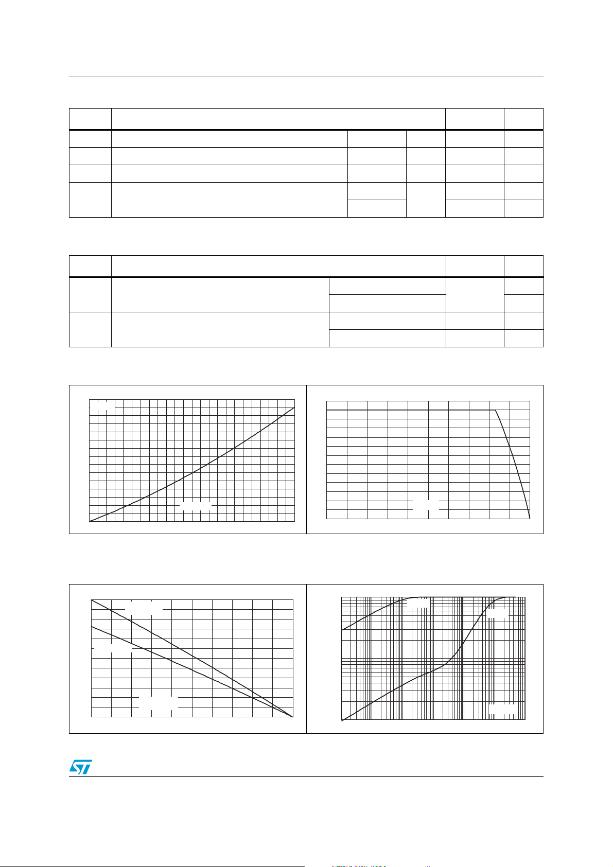
Figure 2. Maximum power dissipation versus
15
14
13
12
11
10
9
8
7
6
5
4
3
2
1
0
Figure 4. On-state rms current versus
Junction to ambient
th(j-a)
on-state rms current (full cycle)
P(W)
α
=180
°
I (A)
T(RMS)
0123456789101112
ambient temperature (free air
2
D
PAK with 1 cm2 of Cu 45 °C/W
Figure 3. On-state rms current versus case
temperature (full cycle)
(A)
I
T(RMS)
13
12
11
10
9
8
7
6
5
4
3
2
1
0
0 25 50 75 100 125
TC(°C)TC(°C)
Figure 5. Relative variation of thermal
impedance versus pulse duration
convection full cycle)
I
(A)
T(RMS)
3.0
2.5
D2PAK
With 1cm
2
of cu
1.0E+00
K=[Zth/Rth]
Z
(j
c)
-
th
Z
(j
a)
-
th
2.0
TO-220AB
1.5
1.0
0.5
0.0
0 25 50 75 100 125
T
(°C)
amb
Doc ID 15238 Rev 4 3/13
1.0E-01
tp(s)
1.0E-02
1.0E-03 1.0E-02 1.0E-01 1.0E+00 1.0E+01 1.0E+02 1.0E+03
Characteristics ACST12
I
(A)
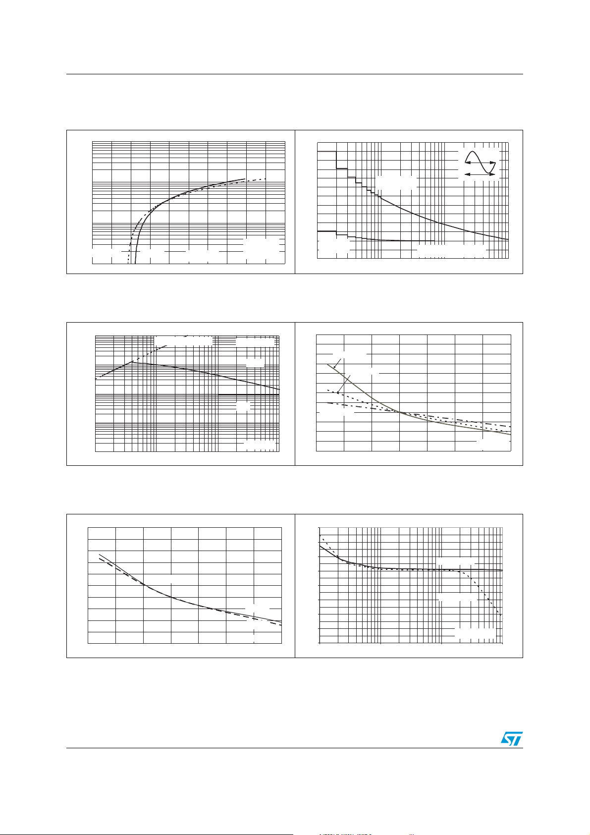
Figure 6. On-state characteristics
(maximum values)
TM
1000
100
10
Tjmax :
V
= 0.90 V
to
R
d
= 30 mΩ
1
Tj=125 °C
Tj=25 °C
VTM(V)
Figure 8. Non repetitive surge peak on-state
current for a sinusoidal pulse and
2
t
Tjinitial=25 °C
I
TSM
10000
1000
corresponding value of I
22
I (A), I t (A s)
TSM
dI/dt limitation: 100 A/µs
Figure 7. Non repetitive surge peak on-state
current versus number of cycles
(T
initial = 25 °C)
j
I(A)
TSM
130
120
110
100
90
80
70
60
50
40
30
20
Repetitive
T
=104 °C
10
C
0
1 10 100 1000
Non repetitive
initial=25 °C
T
j
Number of cycles
t=20ms
One cycle
Figure 9. Relative variation of gate triggering
current and gate voltage versus
junction temperature (typical value)
I , V [T] / I , V [T = 25 °C]
GT GT j GT GT j
3.0
2.5
2.0
IGTQ3
IGTQ1-Q2
100
I²t
10
1
0.01 0.10 1.00 10.00
tP(ms)
Figure 10. Relative variation of holding
current (I
) and latching current (IL)
H
versus junction temperature
I ,I [T ]/I , I [T = 25 °C]
H L j H L j
2.5
2.0
1.5
1.0
0.5
0.0
-50 -25 0 25 50 75 100 125
Typical values
I
L
I
H
Tj(°C)
1.5
VGTQ1-Q2-Q3
1.0
0.5
0.0
-50
-25 0 25 50 75 100 125
Tj(°C)
Figure 11. Relative variation of critical rate of
decrease of main current (di/dt)c
versus (dV/dt)c
(di/dt)c[(dV/dt)c] / Specified(di/dt)c
1.6
1.4
1.2
1.0
0.8
0.6
0.4
0.2
0.0
0.1 1 10 100
ACST12-7Cxx
ACST12-7Sxx
(dV/dt)c (V/µs)
4/13 Doc ID 15238 Rev 4
 Loading...