

®
ASD™
AC Switch Family
MAIN APPLICATIONS
AC static switching in appliance control systems
■
Drive of low power high inductive or resistive
■
loads like
- relay, valve, solenoid, dispenser
- pump, fan, micro-motor
- defrost heater
FEATURES
Blocking voltage : V
■
Avalanche controlled : VCLtyp = 1100 V
■
Nominal conducting current : I
■
Gate triggering current : IGT<10mA
■
■ Switch integrated driver
■ High noise immunity : static dV/dt >500V/µs
DRM/VRRM
= +/-700V
T(RMS)
=2A
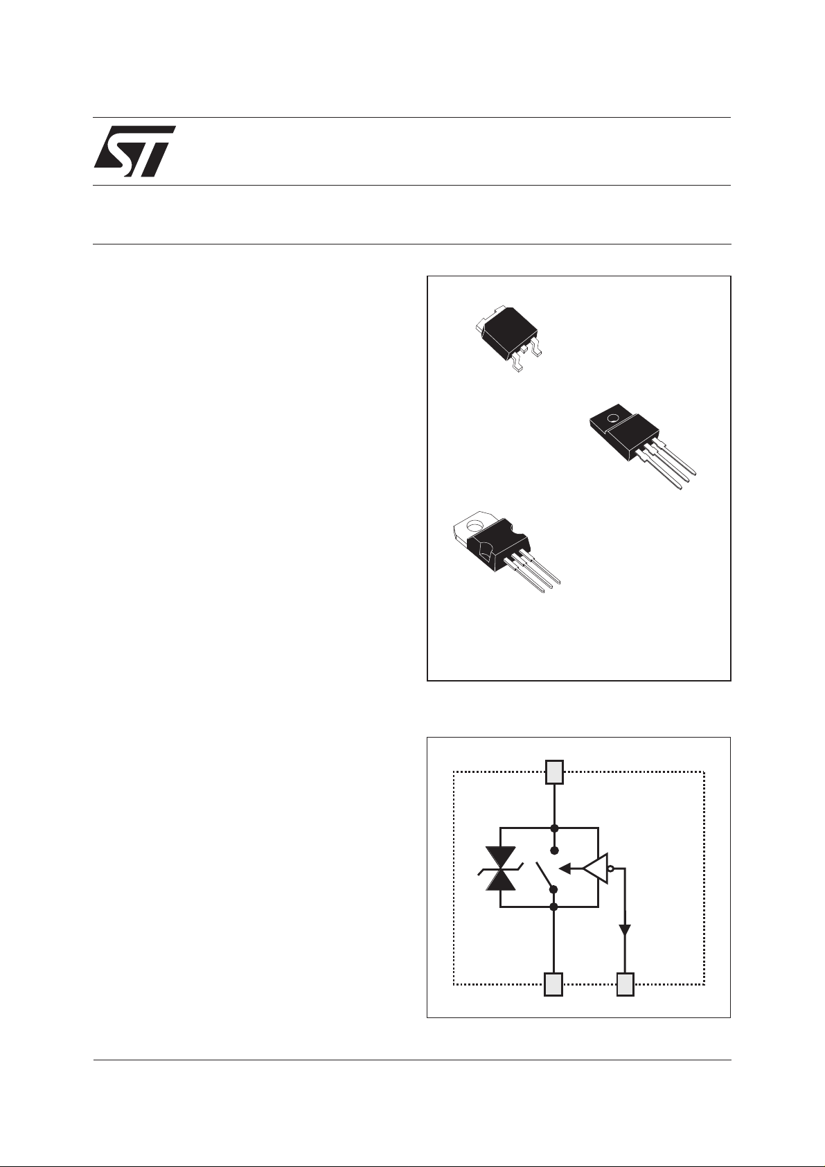
ACS120-7SB/SFP/ST
AC LINE SWITCH
COM
G
OUT
DPAK
ACS120-7SB
G
COM
OUT
TO-220FPAB
ACS120-7SFP
BENEFITS
■ Needs no more external protection snubber or
varistor
■
Enables equipment to meet IEC 61000-4-5
■
Reduces component count up to 80 %
■
Interfaces directly with the microcontroller
■
Eliminates any gate kick back on the
microcontroller
■
Allows straightforward connection of several
ACS™ on same cooling pad.
DESCRIPTION
The ACS120 belongs to the AC line switch family
built around the ASD™ concept. This high performanceswitchcircuitisableto control a loadup to 2
A.
The ACS™ switch embeds a high voltage clampingstructure to absorb the inductiveturnoff energy
anda gate level shifterdriver to separate thedigital
controller from the main switch. It is triggered with
a negative gate current flowing out of the gate pin.
G
COM
OUT
TO-220AB
ACS120-7ST
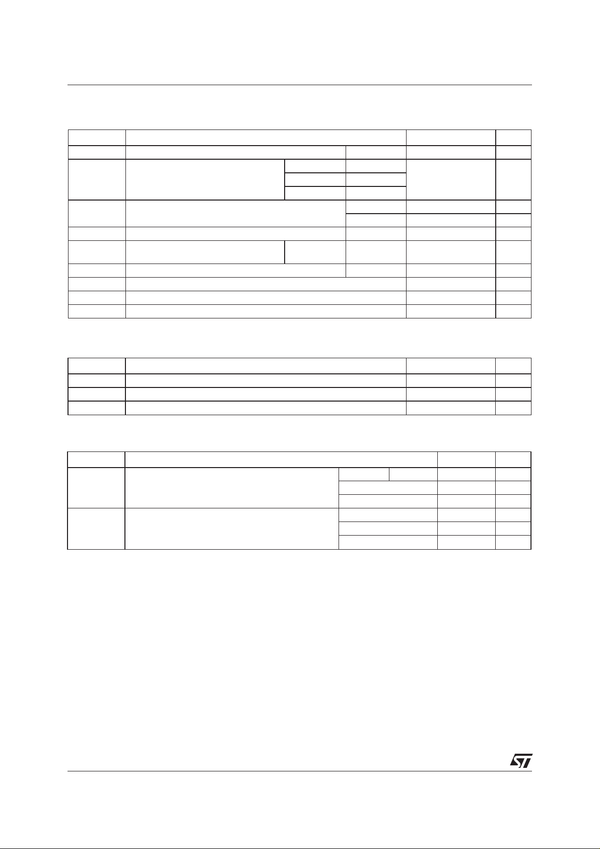
FUNCTIONAL DIAGRAM
OUT
S
ON
D
April 2003 - Ed: 2A
COM
G
1/11
ACS120-7SB/SFP/ST
ABSOLUTE RATINGS (limiting values)
For either positive or negative polarity of pin OUT voltage in respect to pin COM voltage
Symbol Parameter Value Unit
V
DRM/VRRM
I
T(RMS)
I
TSM
2
I
t Fusing capability tp = 10ms 2.2 A²s
dI/dt Repetitiveon-state current critical rate
V
PP
Tstg Storagetemperature range - 40 to + 150 °C
Tj Operating junction temperature range - 30 to + 125 °C
Tl Maximum lead soldering temperature during 10s 260 °C
Note 1: according to test described by IEC61000-4-5 standard & Figure 3.
GATE CHARACTERISTICS (maximum values)
Symbol Parameter Value Unit
P
G (AV)
I
GM
V
GM
Repetitive peak off-state voltage Tj = -10 °C 700 V
RMS on-state current full cycle sine
wave 50 to 60 Hz
DPAK Tc = 115 °C 2 A
TO-220FPAB Tc = °C
TO-220AB Tc = 115 °C
Non repetitive surge peak on-state current
Tj initial = 25°C, full cycle sine wave
of rise I
= 10mA (tr < 100ns)
G
Non repetitive line peak pulse voltage
Tj = 125°C
F =50 Hz 20 A
F =60 Hz 11 A
F = 120 Hz 50 A/µs
note 1
2kV
Average gate power dissipation 0.1 W
Peak gate current (tp = 20µs) 1 A
Peak positive gate voltage (in respect to pin COM) 5 V
THERMAL RESISTANCES
Symbol Parameter Value Unit
Rth (j-a) Junctionto ambient S = 0.5cm² DPAK 70 °C/W
TO-220FPAB 60 °C/W
TO-220AB 60 °C/W
Rth (j-l) Junction to tab/lead for full cycle sine wave
conduction
S = Copper surface under Tab
DPAK 2.6 °C/W
TO-220FPAB 3.5 °C/W
TO-220AB 2.6 °C/W
2/11
PARAMETER DESCRIPTION
Parameter Symbol Parameter description
ACS120-7SB/SFP/ST
I
GT
V
GT
V
GD
I
H
I
L
V
TM
V
TO
Triggering gate current
Triggering gate voltage
Non-triggering gate voltage
Holding current
Latching current
Peak on-state voltage drop
On state threshold voltage
Rd On state dynamic resistance
I
DRM/IRRM
Maximum forward or reverse leakage current
dV/dt Critical rate of rise of off-state voltage
(dV/dt)c Critical rate of rise of commutating off-state voltage
(dI/dt)c Critical rate of decrease of commutating on-state current
V
CL
I
CL
Clamping voltage
Clamping current
ELECTRICAL CHARACTERISTICS
For either positive or negative polarity of pin OUT voltage in respect to pin COM voltage.
Symbol Test Conditions Values Unit
I
GT
V
GT
V
GD
I
H
I
L
V
TM
V
TO
Rd Tj=125°C MAX 200 mΩ
I
DRM
I
RRM
dV/dt V
(dI/dt)c (dV/dt)c = 20V/µs Tj=125°C MIN 1 A/ms
V
CL
V
=12V (DC) RL=140Ω QII - QIII Tj=25°C MAX 10 mA
OUT
V
=12V (DC) RL=140Ω QII - QIII Tj=25°C MAX 1 V
OUT
V
OUT=VDRMRL
I
= 100mA gate open Tj=25°C MAX 45 mA
OUT
=3.3kΩ Tj=125°C MIN 0.15 V
IG= 20mA Tj=25°C MAX 65 mA
I
= 2.8A tp=380µs Tj=25°C MAX 1.3 V
OUT
Tj=125°C MAX 0.85 V
/
V
= 700V Tj=25°C MAX 2 µA
OUT
Tj=125°C MAX 200
=460V gate open Tj=110°C MIN 500 V/µs
OUT
ICL= 1mA tp=1ms Tj=25°C TYP 1100 V
3/11
ACS120-7SB/SFP/ST
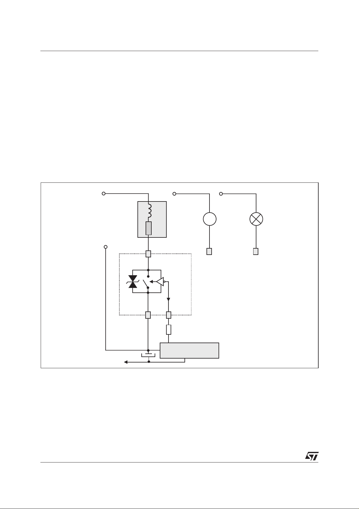
AC LINE SWITCH BASIC APPLICATION
The ACS120 device is well adapted to Washing machine, dishwasher, tumble drier, refrigerator,
air-conditioningsystems, and cookware.Ithas been designedespecially to switchon & off lowpower loads
such as solenoid, valve, relay, dispenser, micro-motor, pump, fan and defrost heaters.
Pin COM: Common drive reference to connect to the power line neutral
Pin G: Switch Gate input to connect to the digital controller
Pin OUT: Switch Output to connect to the load
ThisACS™switch is triggered with anegative gate current flowing outofthe gate pin G. Itcan be driven directly by the digital controller through a resistor as shown on the typical application diagram.
Thanks to its thermal and turn off commutation performances, the ACS120 switch is able to drive with no
turn off additional snubber an inductive load up to 2 A.
TYPICAL APPLICATION DIAGRAM
L
AC
MAINS
N
-Vcc
D
COM
LOAD
L
M
R
OUT
ACS120
S
ON
G
ST72 MCU
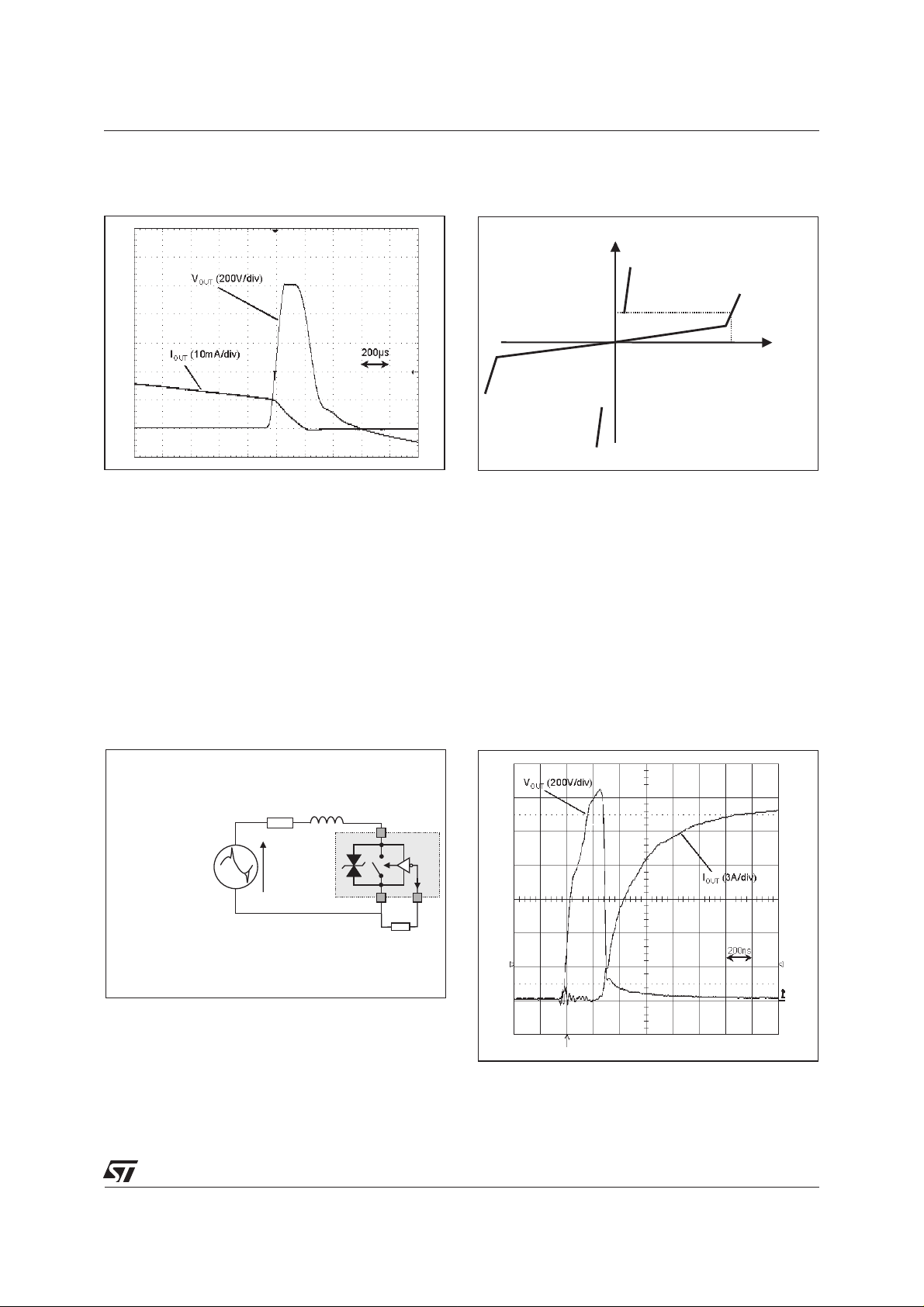
HIGH INDUCTIVE SWITCH-OFF OPERATION
At the end of the last conduction half-cycle, the load current reaches the holding current level I
, and the
H
ACS™ switch turns off. Because of the inductance L of the load, the current flows then through the avalanche diode D and decreases linearly to zero. During this time, the voltage across the switch is limited to
the clamping voltage V
The energy stored in the inductance of the load depends on the holding current I
CL
.
and the inductance (up
H
to10 H); it canreach about 10 mJandis dissipated intheclamping diode section.TheACS switch sustains
the turn off energy because its clamping section is designed for that purpose.
4/11
ACS120-7SB/SFP/ST
Fig. A: Turn-off operation of the ACS120 switch
Fig. B: ACS120 switch static characteristic.
with an electro-valve: waveform of the pin OUT
current I
and voltage V
OUT
OUT
.
IOUT
IH
VCL
AC LINE TRANSIENT VOLTAGE RUGGEDNESS
The ACS120 switch is able to sustain safely the AC line transient voltages either by clamping the low energy spikes or by breaking over under high energy shocks, even with high turn-on current rises.
The test circuit of the figure C is representative of the final ACS application and is also used to stress the
ACS switch according to the IEC 61000-4-5 standard conditions. Thanks to the load, the ACS switch sustains the voltage spikes up to 2 kV above the peak line voltage. It will break over safely even on resistive
load where the turn on current rise is high as shown on figure D. Such non repetitive test can be done 10
times on each AC line voltage polarity.
VOUT
Fig. C: Overvoltage ruggedness test circuit
for resistive and inductive loads according to
IEC61000-4-5 standards.
R = 150Ω, L = 10µH, V
SURGEVOLTAGE
AC LINE & GENERATOR
PP
= 2kV.
R
V
+V
AC
L
OUT
ACSxx
S
PP
ON
D
COM
G
RG = 220Ω
Fig. D: Current and Voltage of the ACS120 dur-
ing IEC61000-4-5 standard test with R,L&V
PP
.
5/11

ACS120-7SB/SFP/ST
OTHER FIGURES
Maximum power dissipation vs RMS on state current.
RMS on-state current vs ambient temperature, case temperature
Relative variation of thermal impedance junction to ambient vs pulse duration and package
Relative variation of gate trigger current vs junction temperature
Relative variation of holding, latching and gate current vs junction
Relative variation of dV/dt vs Tj
Relative variation of (dV/dt)
Surge peak on-state current vs number of cycles
Non repetitive surge peak on-state current for a sinusoidal pulse with tp<10ms, and corresponding of I²t.
On-state characteristics (maximal values)
Thermal resistance junction to ambient vs copper surface under tab (DPAK)
Relative variation of critical (di/dt)c vs junction temperature
vs (di/dt)
c
c
Fig. 1: Maximum power dissipation versus RMS
on-state current.
P(W)
2.4
α=180°
2.2
2.0
1.8
1.6
1.4
1.2
1.0
0.8
0.6
0.4
0.2
0.0
0.0 0.2 0.4 0.6 0.8 1.0 1.2 1.4 1.6 1.8 2.0
I (A)
T(RMS)
180°
α
α
Fig. 2-2: RMS on-state current versus ambient
temperature.
I (A)
T(RMS)
1.8
1.6
1.4
1.2
1.0
0.8
0.6
0.4
0.2
0.0
0 25 50 75 100 125
T (°C)
amb
α=180°
Printed circuitboardFR4
Natural convection
S=0.5cm²
Fig. 2-1: RMS on-state current versus case
temperature.
I (A)
T(RMS)
2.4
α=180°
2.2
2.0
1.8
1.6
1.4
1.2
1.0
0.8
0.6
0.4
0.2
0.0
0 25 50 75 100 125
Tc(°C)
TO-220AB/DPAK
TO-220FPAB
Fig. 3: Relative variation of thermal impedance
versus pulse duration.
K=[Zth/Rth]
1.E+00
DPAK
1.E-01
1.E-02
1.E-02 1.E-01 1.E+00 1.E+01 1.E+02 1.E+03
Zth
(j-c)
TO-220FPAB
DPAK
Zth
(j-a)
t (s)
p
TO-220FPAB
6/11

ACS120-7SB/SFP/ST
Fig. 4: Relative variation of gate trigger current,
holding current and latching versus junction
temperature (typical values).
I , I , I [T ] / I , I , I [T = 25°C]
GTHLj GTHL j
4.0
3.5
3.0
2.5
2.0
1.5
1.0
0.5
0.0
I
GT
I& I
LH
T (°C)
j
-40 -30 -20 -10 0 10 20 30 40 50 60 70 80 90 100 110 120 130
Fig. 6: Relative variation of critical rate of decrease of main current versus reapplied dV/dt
(typical values).
(dI/dt) [(dV/dt) ] / Specified (dI/dt)
5.0
4.5
4.0
3.5
3.0
2.5
2.0
1.5
1.0
0.5
0.0
cc c
V
=400V
OUT
(dV/dt) (V/µs)
c
0 5 10 15 20 25 30 35 40 45 50
Fig. 5: Relative variation of static dV/dt versus
junction temperature.
dV/dt [T ] / dV/dt [T = 125°C]
8
7
6
5
4
3
2
1
0
jj
V
=460V
OUT
T (°C)
j
25 50 75 100 125
Fig. 7: Relative variation of critical rate of decrease
of main current versus junction temperature.
(dI/dt) [Tj] / (dI/dt) [T = 125°C]
ccj
20
18
16
14
12
10
8
6
4
2
0
25 50 75 100 125
T (°C)
j
V
=400V
OUT
Fig. 8: Surge peak on-statecurrentversus number
of cycles.
I (A)
TSM
22
20
18
16
14
12
10
8
6
4
2
0
1 10 100 1000
Repetitive
T =105°C
ab
Non repetitive
T initial=25°C
j
Number of cycles
t=20ms
Fig. 9: Non repetitive surgepeak on-state current
for a sinusoidal pulse with width tp < 10ms, and
corresponding value of I²t.
I (A),I²t (A²s)
TSM
1000
dI/dt limitation:
50A/µS
100
10
t (ms)
p
1
0.01 0.10 1.00 10.00
T initial=25°C
j
I
TSM
I²t
7/11

ACS120-7SB/SFP/ST
Fig. 10: On-state characteristics (maximum
values).
I (A)
TM
10.00
T max. :
j
V =0.85V
to
Ω
R =200m
d
1.00
Tj=125°C
0.10
0.01
0.0 0.5 1.0 1.5 2.0 2.5 3.0 3.5
Tj=25°C
V (V)
TM
ORDERING INFORMATION
ACS 1 20 - 7 S X
AC Switch
Number of switches
Fig. 11: Thermal resistance junction to ambient
versus copper surface under tab (printed circuit
board FR4, copper thickness: 35µm)
Rth (°C/W)
(j-a)
100
90
80
70
60
50
40
30
20
10
0
0 5 10 15 20 25 30 35 40
S(cm²)
Package
V
DRM
7 = 700V
B = DPAK
FP = TO-220FPAB
T = TO-220AB
DPAK
T(RMS)
I
20 = 2.0A
Gate Sensitivity
S= 10mA
8/11

PACKAGE OUTLINE MECHANICAL DATA
DPAK
ACS120-7SB/SFP/ST
DIMENSIONS
REF.
A 2.20 2.40 0.086 0.094
A1 0.90 1.10 0.035 0.043
A2 0.03 0.23 0.001 0.009
B 0.64 0.90 0.025 0.035
B2 5.20 5.40 0.204 0.212
C 0.45 0.60 0.017 0.023
C2 0.48 0.60 0.018 0.023
D 6.00 6.20 0.236 0.244
E 6.40 6.60 0.251 0.259
G 4.40 4.60 0.173 0.181
H 9.35 10.10 0.368 0.397
L2 0.80 typ. 0.031 typ.
L4 0.60 1.00 0.023 0.039
V2 0° 8° 0° 8°
Millimeters Inches
Min. Max Min. Max.
FOOT PRINT
DPAK
6.7
6.7
3
3
1.61.6
2.32.3
9/11

ACS120-7SB/SFP/ST
PACKAGE OUTLINE MECHANICAL DATA
TO-220FPAB
DIMENSIONS
L3
L4
L2
G1
REF.
A
H
B
A 4.4 4.6 0.173 0.181
Millimeters Inches
Min. Max. Min. Max.
B 2.5 2.7 0.098 0.106
Dia
D 2.5 2.75 0.098 0.108
E 0.45 0.70 0.018 0.027
L6
L7
F 0.75 1 0.030 0.039
F1 1.15 1.70 0.045 0.067
F2 1.15 1.70 0.045 0.067
L5
D
F1
F2
G 4.95 5.20 0.195 0.205
G1 2.4 2.7 0.094 0.106
H 10 10.4 0.393 0.409
L2 16 Typ. 0.63 Typ.
L3 28.6 30.6 1.126 1.205
F
E
L4 9.8 10.6 0.386 0.417
L5 2.9 3.6 0.114 0.142
G
L6 15.9 16.4 0.626 0.646
L7 9.00 9.30 0.354 0.366
10/11

PACKAGE OUTLINE MECHANICAL DATA
TO-220AB
H2
L2
F1
Dia
L5
L6
F2
L9
L4
F
G1
G
C
D
M
ACS120-7SB/SFP/ST
DIMENSIONS
REF.
A
L7
E
A 4.40 4.60 0.173 0.181
C 1.23 1.32 0.048 0.051
D 2.40 2.72 0.094 0.107
E 0.49 0.70 0.019 0.027
F 0.61 0.88 0.024 0.034
F1 1.14 1.70 0.044 0.066
F2 1.14 1.70 0.044 0.066
G 4.95 5.15 0.194 0.202
G1 2.40 2.70 0.094 0.106
H2 10 10.40 0.393 0.409
L2 16.4 typ. 0.645 typ.
L4 13 14 0.511 0.551
L5 2.65 2.95 0.104 0.116
L6 15.25 15.75 0.600 0.620
L7 6.20 6.60 0.244 0.259
L9 3.50 3.93 0.137 0.154
M 2.6 typ. 0.102 typ.
Diam. 3.75 3.85 0.147 0.151
Millimeters Inches
Min. Max. Min. Max.
OTHER INFORMATION
Ordering type Marking Package Weight Base qty Delivery mode
ACS120-7SB ACS1207S DPAK 0.3 g 75 Tube
ACS120-7SB-TR ACS1207S DPAK 0.3 g 2500 Tape & reel
ACS120-7SFP ACS1207S TO-220FPAB 2.4 g 50 Tube
ACS120-7ST ACS1207S TO-220AB 2.3 g 250 Bulk
■
Epoxy meets UL94,V0
Informationfurnished is believed to beaccurate and reliable. However, STMicroelectronicsassumesno responsibility for theconsequencesof
useof such information norfor any infringement of patentsor other rights ofthirdparties which may resultfrom its use. No licenseis granted by
implication or otherwise under any patent or patent rights of STMicroelectronics. Specifications mentioned in this publication are subject to
change without notice. This publication supersedes and replaces all information previously supplied.
STMicroelectronics products are not authorized for use as critical components in life support devices or systems without express written approval of STMicroelectronics.
The ST logo is a registered trademark of STMicroelectronics
© 2003 STMicroelectronics - Printed in Italy - All rights reserved.
STMicroelectronics GROUP OF COMPANIES
Australia - Brazil - Canada - China - Finland - France - Germany
Hong Kong - India - Israel - Italy - Japan - Malaysia - Malta - Morocco - Singapore
Spain - Sweden - Switzerland - United Kingdom - United States.
http://www.st.com
11/11
 Loading...