®
ASD™
AC Switch Family
MAIN APPLICATIONS
AC static switching in appliance control systems
■
Drive of low power high inductive or resistive
■
loads like
- relay, valve, solenoid, dispenser
- pump, fan, micro-motor
- defrost heater
ACS110-7SN/SB2
AC LINE SWITCH
COM
OUT
COM
G
FEATURES
Blocking voltage : V
■
Avalanche controlled : VCLtyp = 1100 V
■
Nominal conducting current : I
■
Gate triggering current : IGT<10mA
■
■ Switch integrated driver
■ High noise immunity : static dV/dt >500V/µs
DRM/VRRM
= +/-700V
T(RMS)
=1A
BENEFITS
■ No external protection snubber or varistor
needed
■
Enables equipment to meet IEC 61000-4-5 &
IEC 335-1 (DIL-8 package)
■
Reduces component count up to 80 %
■
Interfaces directly with the microcontroller
■
Eliminates any gate kick back on the
microcontroller
■
Allows straightforward connection of several
ACS™ on same cooling pad (SOT-223)
DESCRIPTION
The ACS110 belongs to the AC line switch family
built around the ASD™ concept. This high performanceswitchcircuitisableto control a loadup to 1
A.
The ACS™ switch embeds a high voltage clampingstructure to absorb the inductiveturnoff energy
anda gate level shifterdriver to separate thedigital
controller from the main switch. It is triggered with
a negative gate current flowing out of the gate pin.
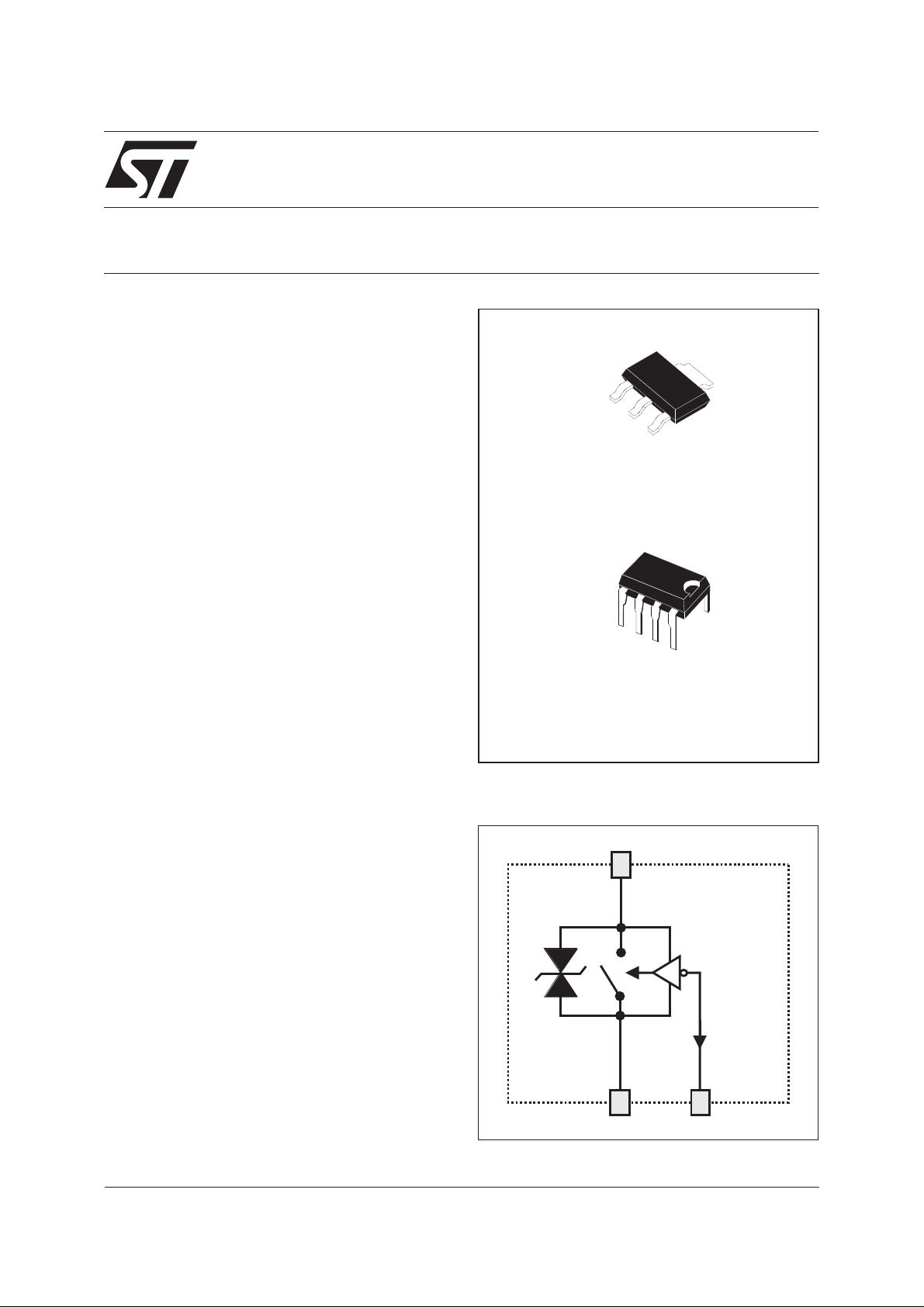
SOT-223
ACS110-7SN
COM
COM
COM
ACS110-7SB2
FUNCTIONAL DIAGRAM
OUT
S
ON
D
G
OUT
COM
DIL-8
April 2003 - Ed: 2A
COM
G
1/10

ACS110-7SN/SB2
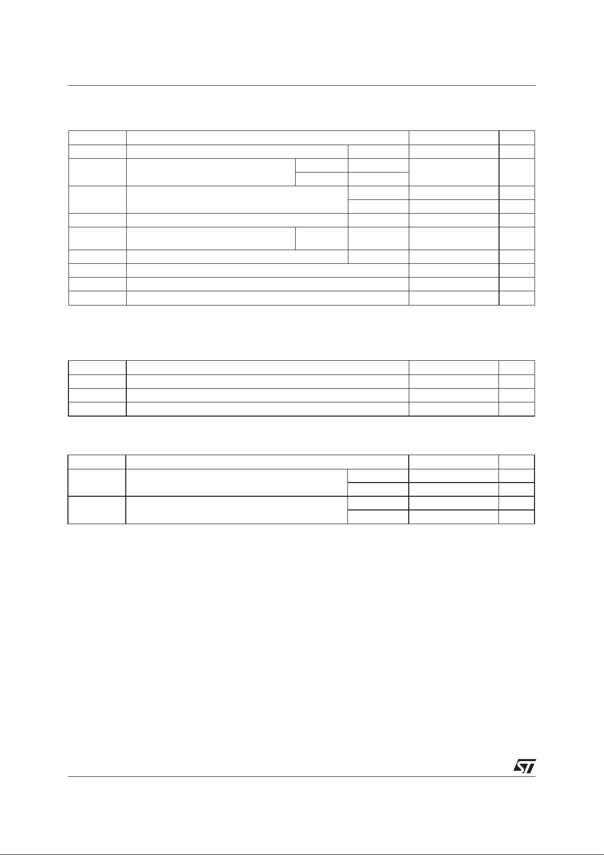
ABSOLUTE RATINGS (limiting values)
For either positive or negative polarity of pin OUT voltage in respect to pin COM voltage
Symbol Parameter Value Unit
V
DRM/VRRM
I
T(RMS)
I
TSM
2
I
t Fusing capability tp = 10ms 0.35 A²s
dI/dt Repetitive on-state current critical rate of
V
PP
Tstg Storage temperature range - 40 to + 150 °C
Tj Operating junction temperature range - 30 to + 125 °C
Tl Maximum lead soldering temperature during 10s 260 °C
Note 1: according to test described by IEC61000-4-5 standard & Figure 3.
GATE CHARACTERISTICS (maximum values)
Symbol Parameter Value Unit
P
G (AV)
I
GM
V
GM
Repetitive peak off-state voltage Tj = -10 °C 700 V
RMS on-state current full cycle sine wave
50 to 60 Hz
Non repetitive surge peak on-state current
Tj initial = 25°C, full cycle sine wave
rise I
= 10mA (tr < 100ns)
G
Non repetitive line peak pulse voltage
SOT-223 Ttab = 105 °C 1 A
DIL-8 Tlead = 110 °C
F =50 Hz 8 A
F =60 Hz 11 A
Tj = 125°C
F = 120 Hz 50 A/µs
note 1
2kV
Average gate power dissipation 0.1 W
Peak gate current (tp = 20µs) 1 A
Peak positive gate voltage (in respect to pin COM) 5 V
THERMAL RESISTANCES
Symbol Parameter Value Unit
Rth (j-a) Junction to ambient S = 5cm² SOT-223 60 °C/W
DIL-8 60 °C/W
Rth (j-l) Junction to tab/lead for full cycle sine wave conduction SOT-223 20 °C/W
DIL-8 15 °C/W
S = Copper surface under Tab
2/10

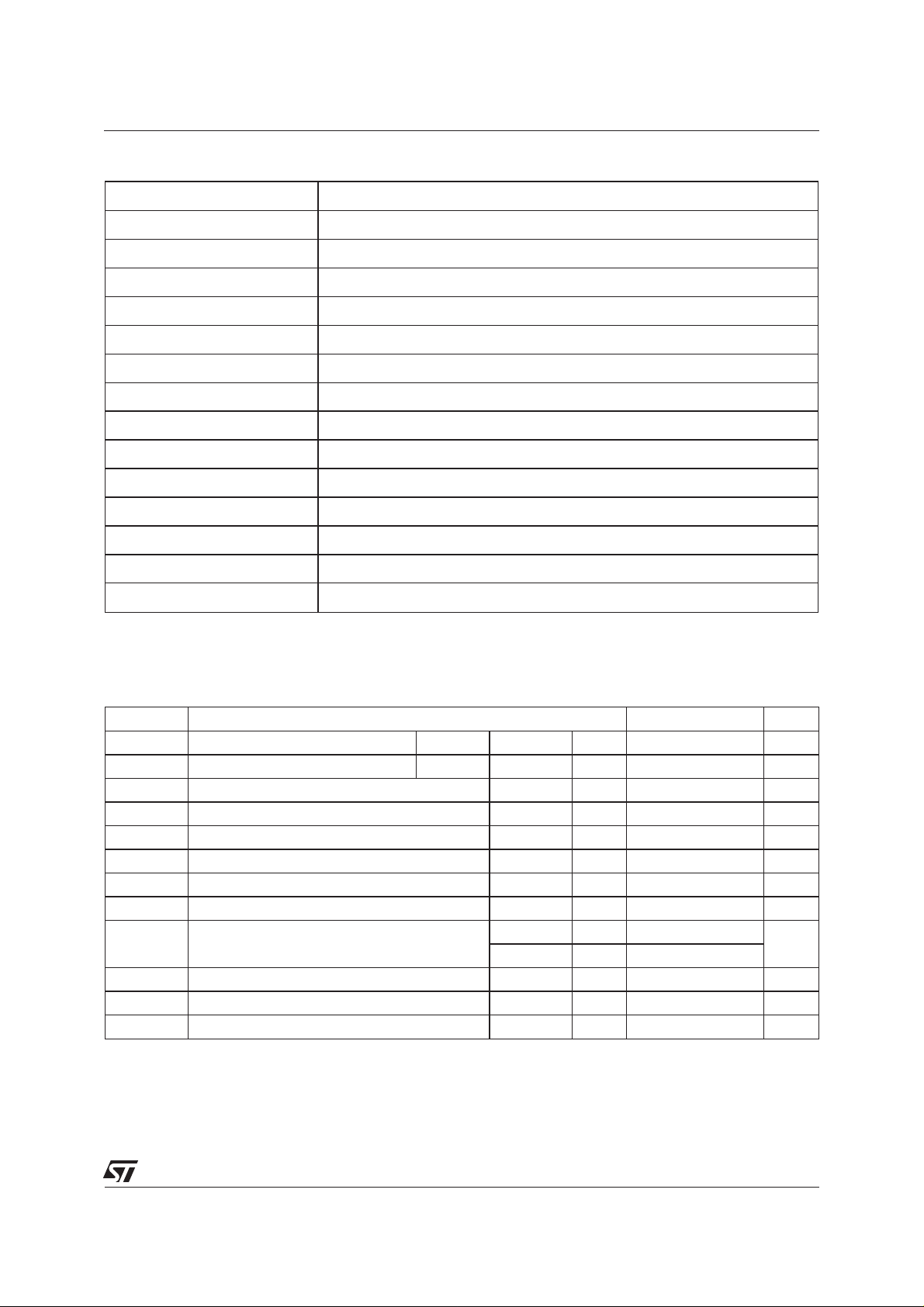
PARAMETER DESCRIPTION
Parameter Symbol Parameter description
ACS110-7SN/SB2
I
GT
V
GT
V
GD
I
H
I
L
V
TM
V
TO
Triggering gate current
Triggering gate voltage
Non-triggering gate voltage
Holding current
Latching current
Peak on-state voltage drop
On state threshold voltage
Rd On state dynamic resistance
I
DRM/IRRM
Maximum forward or reverse leakage current
dV/dt Critical rate of rise of off-state voltage
(dV/dt)c Critical rate of rise of commutating off-state voltage
(dI/dt)c Critical rate of decrease of commutating on-state current
V
CL
I
CL
Clamping voltage
Clamping current
ELECTRICAL CHARACTERISTICS
For either positive or negative polarity of pin OUT voltage respect to pin COM voltage excepted note 3*.
Symbol Test Conditions Values Unit
I
GT
V
GT
V
GD
I
H
I
L
V
TM
V
TO
V
=12V (DC) RL=140Ω QII - QIII Tj=25°C MAX 10 mA
OUT
V
=12V (DC) RL=140Ω QII - QIII Tj=25°C MAX 1 V
OUT
V
OUT=VDRMRL
I
= 100mA gate open Tj=25°C MAX 45 mA
OUT
=3.3kΩ Tj=125°C MIN 0.15 V
IG= 20mA Tj=25°C MAX 65 mA
I
= 1.4A tp=380µs Tj=25°C MAX 1.3 V
OUT
Tj=125°C MAX 0.8 V
Rd Tj=125°C MAX 300 mΩ
/
V
I
DRM
I
RRM
dV/dt V
= 700V Tj=25°C MAX 2 µA
OUT
Tj=125°C MAX 200
=460V gate open Tj=110°C MIN 500 V/µs
OUT
(dI/dt)c (dV/dt)c = 20V/µs Tj=125°C MIN 0.5 A/ms
V
CL
ICL= 1mA tp=1ms Tj=25°C TYP 1100 V
3/10
 Loading...