

Transient protected AC switch (ACS™)
Features
■ Needs no external protection snubber or
varistor
■ Enables equipment to meet IEC 61000-4-5
■ Reduces component count by up to 80%
■ Interfaces directly with the microcontroller
■ Common package tab connection supports
connection of several alternating current
switches (ACS) on the same cooling pad
■ Integrated structure based on ASD technology
■ Overvoltage protection by crowbar technology
■ High noise immunity - static dV/dt > 300 V/µs
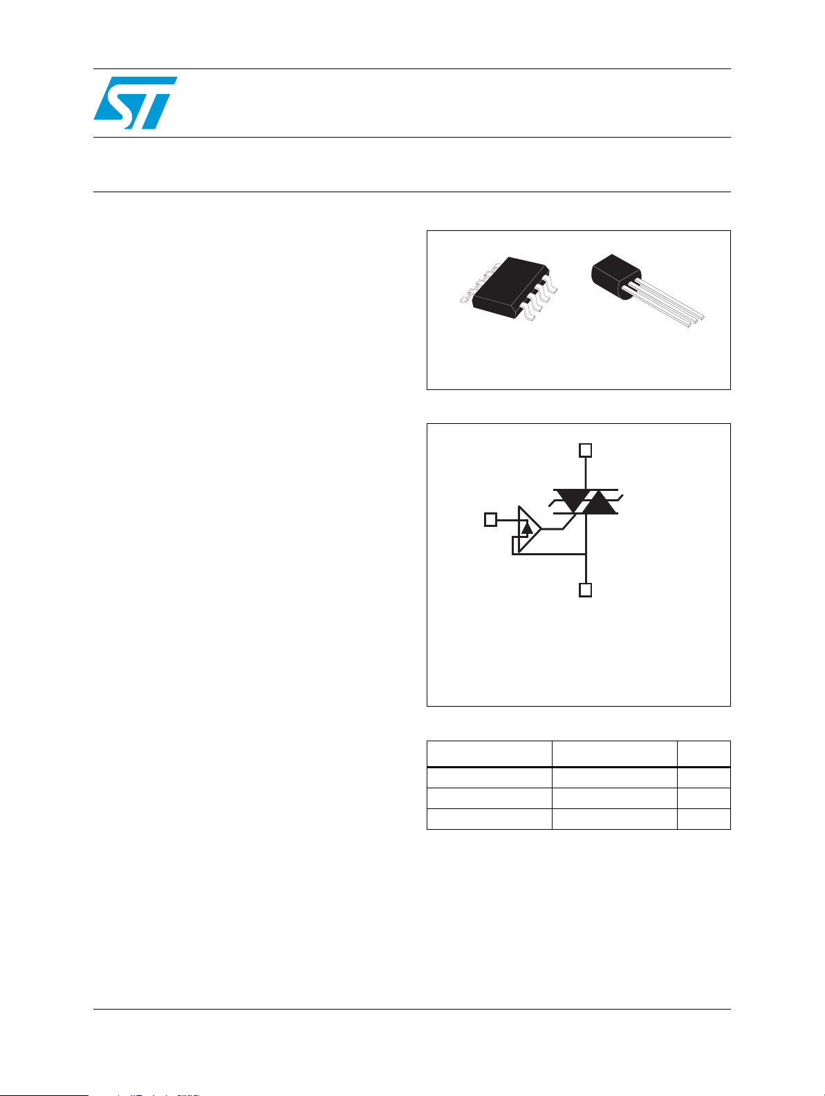
ACS102-6T
G (5)
COM (6)
COM (7)
NC (8)
SO-8
ACS102-6T1
Figure 1. Functional diagram
NC (4)
NC (3)
OUT (2)
NC (1)
ACS102-6TA
OUT
TO-92
OUT
COM
G
Applications
■ Alternating current on/off static switching in
appliances and industrial control systems
■ Drive of low-power, high-inductive or resistive
loads like:
– relay, valve, solenoid
– dispenser, door lock
– micro-motor
Description
The ACS102-6T belongs to the AC line switch
family. This high performance switch can control a
load of up to 0.2A.
The ACS102-6T switch includes an overvoltage
crowbar structure to absorb the overvoltage
energy, and a gate level shifter driver to separate
the digital controller from the main switch. It is
triggered with a negative gate current flowing out
of the gate pin.
G
COM
COM Common drive reference to connect
to the mains
OUT Output to connect to the load.
G Gate input to connect to the controller
through gate resistor
Table 1. Device summary
Symbol Value Unit
I
T(RMS)
V
DRM/VRRM
I
GT
0.2 A
600 V
5mA
TM: ACS is a trademark of STMicroelectronics
ASD: Application specific devices
May 2011 Doc ID 11961 Rev 3 1/11
www.st.com
11

Characteristics ACS102-6T
1 Characteristics
Table 2. Absolute maximum ratings (T
= 25 °C, unless otherwise specified)
amb
Symbol Parameter Value Unit
I
T(RMS)
I
On-state rms current (full sine wave)
Non repetitive surge peak on-state current
TSM
(full cycle sine wave, Tj initial = 25 °C)
SO-08 T
f = 60 Hz t = 16.7 ms 7.6
f = 50 Hz t = 20 ms 7.3
I²t I²t Value for fusing t
TO-92 T
dI/dt
V
V
P
T
1. According to test described by IEC 61000-4-5 standard and Figure 17
Table 3. Electrical characteristics (Tj = 25 °C, unless otherwise specified)
Critical rate of rise of on-state current
I
= 2xIGT, tr ≤ 100 ns
G
Non repetitive line peak mains voltage
PP
I
Peak gate current tp = 20 µs Tj = 125 °C 1 A
GM
Peak positive gate voltage Tj = 125 °C 10 V
GM
Average gate power dissipation Tj = 125 °C 0.1 W
G(AV)
Storage junction temperature range
stg
T
Operating junction temperature range
j
(1)
f = 120 Hz T
= 100 °C
amb
= 100 °C
amb
= 10 ms 0.38 A²s
p
= 125 °C 50 A/µs
j
0.2 A
Tj = 25 °C 2 kV
-40 to +150
-30 to +125
A
°C
Symbol Test conditions Quadrant Value Unit
(1)
I
GT
V
GT
V
GD
(2)
I
H
(2)
I
L
dV/dt
(dI/dt)c
V
CL
1. Minimum IGT is guaranteed at 10% of IGT max
2. For both polarities of OUT referenced to COM
V
= 12 V, RL = 33 Ω
OUT
V
= V
OUT
I
= 100 mA MAX 20 mA
OUT
IG = 1.2 x I
(2)
V
= 67% V
OUT
(2)
Without snubber (15 V/µs), turn-off time ≤ 20 ms, Tj = 125 °C MIN 0.15 A/ms
, RL =3.3 kΩ, Tj = 125 °C II - III MIN 0.15 V
DRM
GT
gate open, Tj = 125 °C MIN 300 V/µs
DRM,
ICL = 0.1 mA, tp = 1 ms, Tj = 125 °C MIN 650 V
II - III MAX 5 mA
II - III MAX 0.9 V
MAX 25 mA
2/11 Doc ID 11961 Rev 3
ACS102-6T Characteristics
Table 4. Static electrical characteristics
Symbol Test conditions Value Unit
(1)
V
V
TM
TO
R
I
DRM
I
RRM
(1)
D
(1)
I
= 0.3 A, tp = 380 µs Tj = 25 °C MAX 1.2 V
TM
Tj = 125 °C MAX 0.80 V
Tj = 125 °C MAX 500 mΩ
V
OUT
= 600 V
Tj = 25 °C
MAX
Tj = 125 °C 0.2 mA
2µA
1. for both polarities of OUT referenced to COM
Table 5. Thermal resistance
Symbol Parameter Value Unit
R
th (j-l)
Junction to lead (AC) TO-92 60
TO-92 150
R
th (j-a)
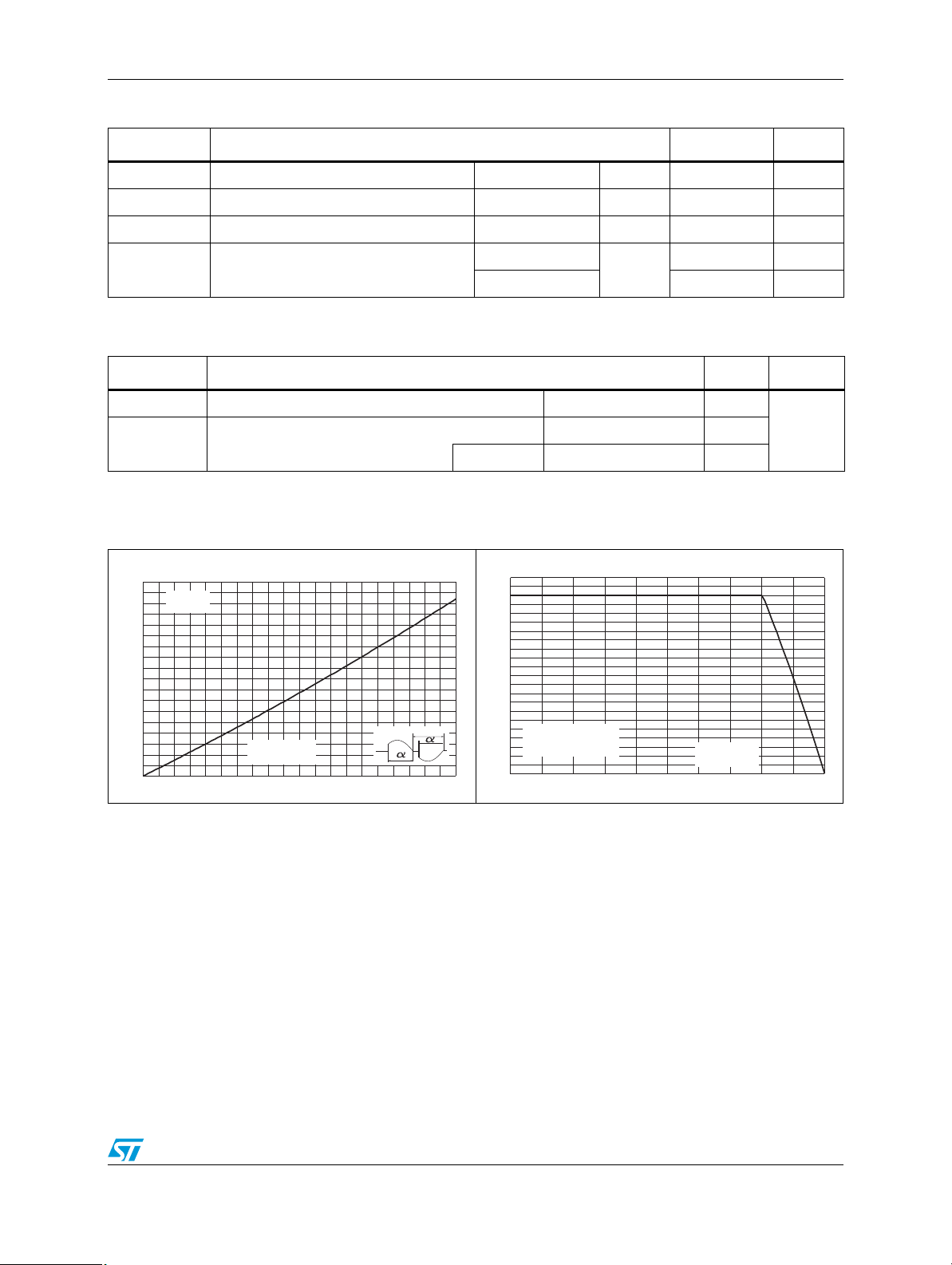
Figure 2. Maximum power dissipation
Junction to ambient
versus on-state rms current
S = 40 mm² SO-8 150
Figure 3. On-state rms current versus
ambient temperature (full cycle)
(full cycle)
P (W)
0.18
0.16
0.14
0.12
0.10
0.08
0.06
0.04
0.02
0.00
α=180°
180°
I (A)
T(RMS)
0.00 0.02 0.04 0.06 0.08 0.10 0.12 0.14 0.16 0.18 0.20
I (A)
T(RMS)
0.22
0.20
0.18
0.16
0.14
0.12
0.10
0.08
0.06
0.04
0.02
0.00
0 25 50 75 100 125
a=180°
Printed circuit board FR4
Natural convection
T°C
amb
°C/W
Doc ID 11961 Rev 3 3/11
Characteristics ACS102-6T
(
)
Figure 4. Relative variation of junction to
ambient thermal impedance versus
pulse duration and package
K=[Z
1.E+00
1.E-01
1.E-02
1.E-03 1.E-02 1.E-01 1.E+00 1.E+01 1.E+02 1.E+03
th(j-a)/Rth(j-a)
TO-9 2
]
SO-8
t (S)
P
Figure 6. Non repetitive surge peak on-state
current versus number of cycles
I
(A)
TSM
10
9
8
7
6
Non repetitive
Tj initial=25°C
5
4
3
Repetitive
T
=100°C
amb
2
1
0
1 10 100 1000
t=20ms
One cycle
Number of cycles
Figure 5. Relative variation of gate trigger,
holding and latching current versus
junction temperature
I
,I
,I
[T
]/I
,I
,I
[T
GT
H
L
IL& I
j
H
2.5
2.0
1.5
1.0
0.5
0.0
-40 -30 -20 -10 0 10 20 30 40 50 60 70 80 90 100 110 120 130
=25°C]
GT
H
L
j
I
GT
Tj(°C)
Figure 7. Non repetitive surge peak on-state
current for a sinusoidal pulse, and
corresponding value of I²t
(A), I²t (A²s)
I
TSM
1.E+03
1.E+02
1.E+01
1.E+00
(ms)t
1.E-01
p
0.01 0.10 1.00 10.00
Tjinitial=25 °C
Pulse width tp< 10 ms
I
TSM
I²t
Figure 8. On-state characteristics
(maximal values)
Figure 9. SO-8 junction to ambient thermal
resistance versus copper surface
under tab
R
I
A
TM
10.00
Tjmax.:
V
= 0.8 V
to
R
= 500 mΩ
d
1.00
Tj=125°C
Tj=25°C
0.10
0.01
VTM(V)
160
140
120
100
80
60
40
20
0.0 0.5 1.0 1.5 2.0 2.5 3.0 3.5 4.0
4/11 Doc ID 11961 Rev 3
(°C/W)
th(j-a)
PCB FR4, copper thickness 35 µm
SCU(mm²)
0
0 50 100 150 200 250 300
SO-8
 Loading...