

Up to 1 A step down switching regulator with adjustable
current limit for automotive applications
Features
■ Qualified following the AEC-Q100
requirements (see PPAP for more details)
■ Up to 1 A DC output current
■ Operating input voltage from 8 V to 36 V
■ Output voltage adjustable from 1.235 V to 35 V
■ Precise 3.3 V (±2 %) reference voltage
■ 250 kHz Internally fixed frequency
■ Voltage feedforward
■ Zero-load current operation
■ Internal current limiting
■ Protection against feedback disconnection
■ Thermal shutdown
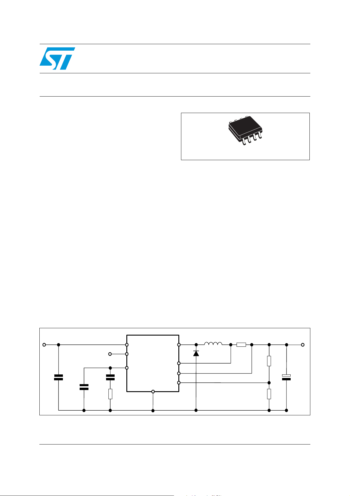
A6902D
SO-8
Applications
■ Automotive applications
■ Adjustable current generator
■ Simple step-down converters with adjustable
current limit
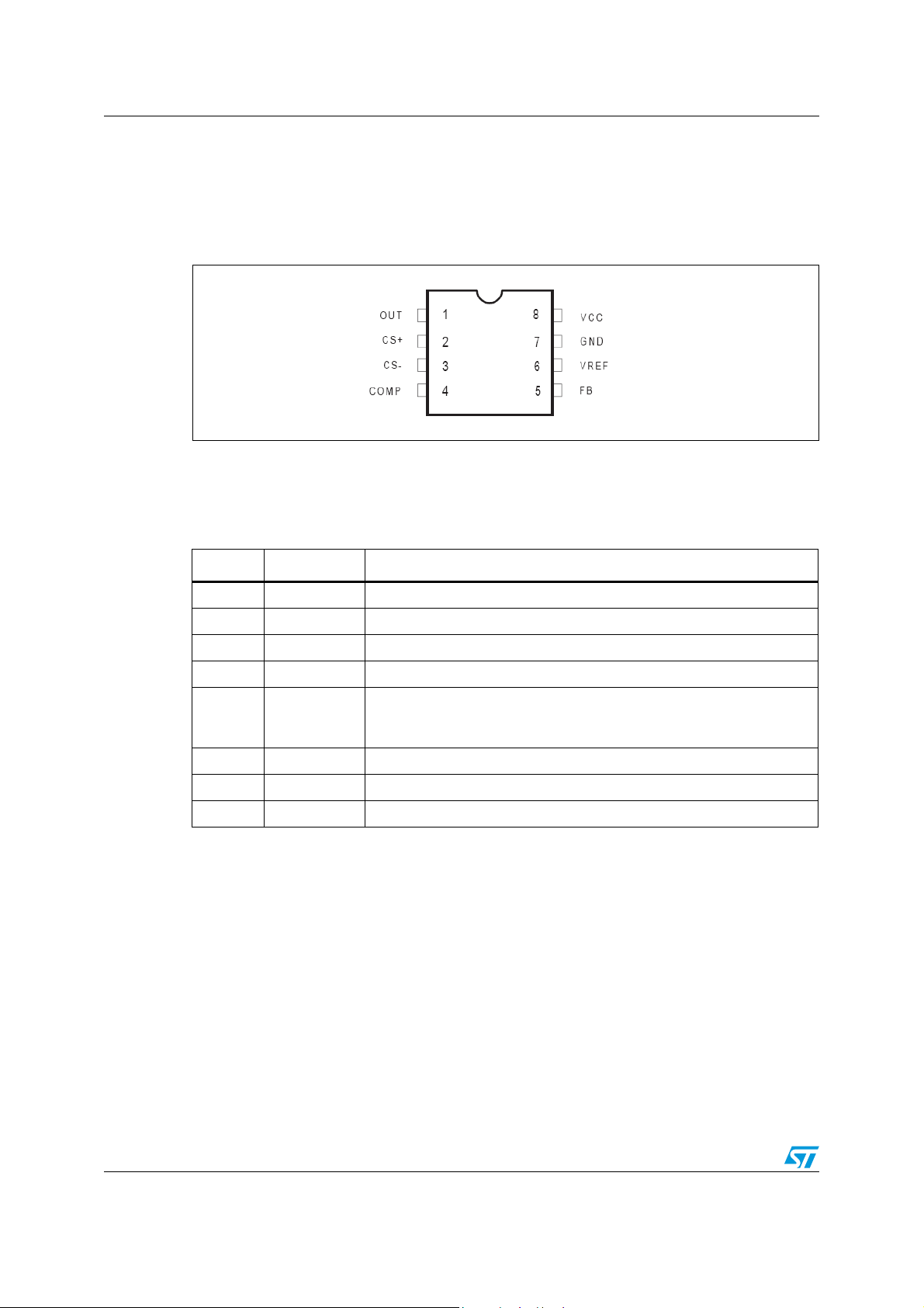
Figure 1. Application schematic
V
V
=8V to 36V
=8V to 36V
IN
IN
=8V to 36V
=8V to 36V
V
V
IN
IN
C1
C1
10µF
10µF
35V
35V
C3
C3
220pF
220pF
C2
C2
22nF
22nF
V
V
CC
CC
V
V
REF
REF
COMP
COMP
R3
R3
5.1kO
5.1kO
L6902D
L6902D
GND
GND
OUT
OUT
CS+
CS+
CS-
CS-
FB
FB
L1 22µH
L1 22µH
D1
D1
STPS340U
STPS340U
Rsense
Rsense
100mO
100mO
V
V
OUT
OUT
R1
R1
5.6kO
5.6kO
R2
R2
3.3kO
3.3kO
=3.3V
=3.3V
C4
C4
100µF
100µF
10V
10V
April 2009 Doc ID 13959 Rev 5 1/12
www.st.com
12

Contents A6902D
Contents
1 Description . . . . . . . . . . . . . . . . . . . . . . . . . . . . . . . . . . . . . . . . . . . . . . . . . 3
2 Pin connection . . . . . . . . . . . . . . . . . . . . . . . . . . . . . . . . . . . . . . . . . . . . . . 4
2.1 Pin connection . . . . . . . . . . . . . . . . . . . . . . . . . . . . . . . . . . . . . . . . . . . . . . 4
2.2 Pin description . . . . . . . . . . . . . . . . . . . . . . . . . . . . . . . . . . . . . . . . . . . . . . 4
3 Electrical data . . . . . . . . . . . . . . . . . . . . . . . . . . . . . . . . . . . . . . . . . . . . . . 5
3.1 Maximum ratings . . . . . . . . . . . . . . . . . . . . . . . . . . . . . . . . . . . . . . . . . . . . 5
3.2 Thermal data . . . . . . . . . . . . . . . . . . . . . . . . . . . . . . . . . . . . . . . . . . . . . . . 5
4 Electrical characteristics . . . . . . . . . . . . . . . . . . . . . . . . . . . . . . . . . . . . . 6
5 Package mechanical data . . . . . . . . . . . . . . . . . . . . . . . . . . . . . . . . . . . . . 8
6 Order codes . . . . . . . . . . . . . . . . . . . . . . . . . . . . . . . . . . . . . . . . . . . . . . . 10
7 Revision history . . . . . . . . . . . . . . . . . . . . . . . . . . . . . . . . . . . . . . . . . . . 11
2/12 Doc ID 13959 Rev 5

A6902D Description
1 Description
The A6902D is a complete and simple step down switching regulator with adjustable current
limit. Based on a voltage mode structure it integrates a current error amplifier to have a
constant voltage and constant current control. By means of an on board current sense
resistor and the availability of the current sense pins (both compatible to Vcc and for Cscompatible with GND too) a current limit programming is very simple and accurate.
Moreover constant current control can be used to charge NiMH and NiCd batteries.The
device can be used as a standard DC/DC converter with adjustable current limit (set by
using the external sense resistor). The internal robust P-channel DMOS transistor with a
typical of 250 mΩ assures high efficiency and a minimum dropout even at high output
current level. The internal limiting current (latched function) of typical value of 2.5 A protects
the device from accidental output short circuit avoiding dangerous loads damage. If the
temperature of the chip goes higher than a fixed internal threshold (150 °C with 20 °C
hysteresis), the power stage is turned off.
Other protections beside thermal shutdown complete the device for a safe and reliable
application: overvoltage protection, frequency folback overcurrent protection and protection
vs. feedback disconnection. The internal fixed switching frequency of 250 kHz, and the
SO-8 package pin allow to built an ultra compact DC/DC converter with a minimum board
space.
Doc ID 13959 Rev 5 3/12
Pin connection A6902D
2 Pin connection
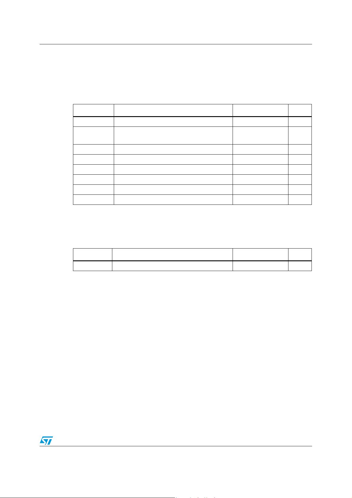
2.1 Pin connection
Figure 2. Pin connection (top view)
2.2 Pin description
Table 1. Pin description
N° Pin Description
1 OUT Regulator output.
2 CS+ Current error amplifier input (current sense at higher voltage)
3 CS- Current error amplifier input (current sense at lower voltage)
4 COMP E/A output for frequency compensation.
Feedback input. Connecting directly to this pin results in an output
5FB
voltage of 1.23 V. An extenal resistive divider is required for higher
output voltages.
6V
REF
3.3 V reference voltage. No cap is need for stability.
7 GND Ground.
8 VCC Unregulated DC input voltage.
4/12 Doc ID 13959 Rev 5
A6902D Electrical data
3 Electrical data
3.1 Maximum ratings
Table 2. Absolute maximum ratings
Symbol Parameter Value Unit
V
8
V
1
I
1
V
, V
4
, V
V
2
P
TOT
T
J
T
STG
Input voltage 40 V
OUT pin DC voltage
OUT pin peak voltage at Δt = 0.1 μs
Maximum output current int. limit.
Analog pins 4 V
5
Analog pins -0.3 to V
3
Power dissipation at T
Operating junction temperature range -40 to 150 °C
Storage temperature range -55 to 150 °C
3.2 Thermal data
Table 3. Thermal data
Symbol Parameter SO8 Unit
R
thJA
1. Package mounted on board
Maximum thermal resistance junction-ambient 110
-1 to 40
-5 to 40
CC
≤ 70 °C 0.7 W
A
(1)
V
V
V
°C/W
Doc ID 13959 Rev 5 5/12

Electrical characteristics A6902D
4 Electrical characteristics
TJ = -40 to 125 °C, V
= 12 V, unless otherwise specified
CC
Table 4. Electrical characteristics
Symbol Parameter Test conditions Min. Typ. Max. Unit
V
CC
R
DS(on)
I
f
SW
Dynamic characteristics (see test circuit)
V
η Efficiency V
DC characteristics
I
qop
I
Error amplifier
Operating input
voltage range
MOSFET on
resistance
Maximum limiting
L
current
(1)
= 1.235 V; I0 = 2 A 8 36 V
V
0
0.250 0.5 Ω
V
= 8.5 V 1.8 2.5 3.2
CC
= 8.5 V, TJ = 25 °C 2 2.5 3.2
V
CC
Switching frequency 212 250 280 kHz
Duty cycle 0 100 %
Voltage feedback
5
8 V < V
20 mA < I0 < 1 A
Total operating
quiescent current
Quiescent current Duty cycle = 0; V
q
= 5 V, V
0
< 36 V,
CC
= 12 V 90 %
CC
1.198 1.235 1.272 V
35mA
= 1.5 V 2.7 mA
FB
A
V
OH
V
OL
I
o source
I
o sink
I
gm Transconductance
V
OFFS
I
CS+
I
CS-
High level output
voltage
Low level output
voltage
Source output current
Sink output current
Source bias current 2.5 4 μA
b
DC open loop gain R
Input offset voltage
CS+ output current
CS- output current
V
FB
V
FB
V
COMP
V
FB
V
COMP
V
FB
L= 50 58 dB
I
COMP
V
COMP
V
CS-
V
CS+
=1 A; R
I
0
V
OUT
=1A; R
I
0
V
OUT
6/12 Doc ID 13959 Rev 5
=1 V 3.6 V
=1.5 V 0.4 V
= 1.9 V;
= 1 V
= 1.9 V;
= 1.5 V
160 300 μA
11.5 mA
8
= -0.1 mA to 0.1 mA;
= 1.9 V
= 1.8 V;
= V
comp
=100 mΩ;
SENSE
< VCC-2 V
=100 mΩ;
SENSE
< VCC-2 V
90 100 110 mV
2.3 mS
1.5 3 μA
1.5 3 μA

A6902D Electrical characteristics
Table 4. Electrical characteristics (continued)
Symbol Parameter Test conditions Min. Typ. Max. Unit
Reference section
I
= 0 to 5 mA
Reference voltage
Line regulation
Load regulation I
Short circuit current 5 18 35 mA
REF
V
= 8 V to 36 V
CC
I
= 0mA
REF
V
= 8 V to 36 V
CC
= 0 to 5 mA 8 15 mV
REF
3.2 3.3 3.399 V
510mV
1. With TJ = 85 °C, I
= 2 A, assured by design, characterization and statistical correlation.
lim_min
Doc ID 13959 Rev 5 7/12

Package mechanical data A6902D
5 Package mechanical data
In order to meet environmental requirements, ST offers these devices in different grades of
ECOPACK
specifications, grade definitions and product status are available at: www.st.com.
ECOPACK
®
packages, depending on their level of environmental compliance. ECOPACK®
®
is an ST trademark.
8/12 Doc ID 13959 Rev 5

A6902D Package mechanical data
Table 5. SO-8 mechanical data
mm inch
Dim
Min. Typ. Max. Min. Typ. Max.
A 1.35 1.75 0.053 0.069
A1 0.10 0.25 0.004 0.010
A2 1.10 1.65 0.043 0.065
B 0.33 0.51 0.013 0.020
C 0.19 0.25 0.007 0.010
(1)
D
E 3.80 4.00 0.15 0.157
e1.27 0.050
H 5.80 6.20 0.228 0.244
h 0.25 0.50 0.010 0.020
L 0.40 1.27 0.016 0.050
k0° (min), 8° (max)
ddd 0.10 0.004
4.80 5.00 0.189 0.197
1. 1. Dimension D does not include mold flash, protrusions or gate burrs. Mold flash, protrusions or gate burrs
shall not exceed 0.15 mm (0.006 inch) in total (both side).
Figure 3. Package dimensions
Doc ID 13959 Rev 5 9/12

Order codes A6902D
6 Order codes
Table 6. Ordering information
Order codes Package Packaging
A6902D
Tu b e
SO-8
A6902D13TR Tape and reel
10/12 Doc ID 13959 Rev 5

A6902D Revision history
7 Revision history
Table 7. Document revision history
Date Revision Changes
02-Oct-2007 1 Initial release
5-Nov-2007 2 Updated: Table 4 on page 6
2-May-2008 3 Updated: Table 4 on page 6
28-Aug-2008 4 Updated: Coverpage and Table 4 on page 6
23-Apr-2009 5 Updated first feature in coverpage
Doc ID 13959 Rev 5 11/12

A6902D
Please Read Carefully:
Information in this document is provided solely in connection with ST products. STMicroelectronics NV and its subsidiaries (“ST”) reserve the
right to make changes, corrections, modifications or improvements, to this document, and the products and services described herein at any
time, without notice.
All ST products are sold pursuant to ST’s terms and conditions of sale.
Purchasers are solely responsible for the choice, selection and use of the ST products and services described herein, and ST assumes no
liability whatsoever relating to the choice, selection or use of the ST products and services described herein.
No license, express or implied, by estoppel or otherwise, to any intellectual property rights is granted under this document. If any part of this
document refers to any third party products or services it shall not be deemed a license grant by ST for the use of such third party products
or services, or any intellectual property contained therein or considered as a warranty covering the use in any manner whatsoever of such
third party products or services or any intellectual property contained therein.
UNLESS OTHERWISE SET FORTH IN ST’S TERMS AND CONDITIONS OF SALE ST DISCLAIMS ANY EXPRESS OR IMPLIED
WARRANTY WITH RESPECT TO THE USE AND/OR SALE OF ST PRODUCTS INCLUDING WITHOUT LIMITATION IMPLIED
WARRANTIES OF MERCHANTABILITY, FITNESS FOR A PARTICULAR PURPOSE (AND THEIR EQUIVALENTS UNDER THE LAWS
OF ANY JURISDICTION), OR INFRINGEMENT OF ANY PATENT, COPYRIGHT OR OTHER INTELLECTUAL PROPERTY RIGHT.
UNLESS EXPRESSLY APPROVED IN WRITING BY AN AUTHORIZED ST REPRESENTATIVE, ST PRODUCTS ARE NOT
RECOMMENDED, AUTHORIZED OR WARRANTED FOR USE IN MILITARY, AIR CRAFT, SPACE, LIFE SAVING, OR LIFE SUSTAINING
APPLICATIONS, NOR IN PRODUCTS OR SYSTEMS WHERE FAILURE OR MALFUNCTION MAY RESULT IN PERSONAL INJURY,
DEATH, OR SEVERE PROPERTY OR ENVIRONMENTAL DAMAGE. ST PRODUCTS WHICH ARE NOT SPECIFIED AS "AUTOMOTIVE
GRADE" MAY ONLY BE USED IN AUTOMOTIVE APPLICATIONS AT USER’S OWN RISK.
Resale of ST products with provisions different from the statements and/or technical features set forth in this document shall immediately void
any warranty granted by ST for the ST product or service described herein and shall not create or extend in any manner whatsoever, any
liability of ST.
ST and the ST logo are trademarks or registered trademarks of ST in various countries.
Information in this document supersedes and replaces all information previously supplied.
The ST logo is a registered trademark of STMicroelectronics. All other names are the property of their respective owners.
© 2009 STMicroelectronics - All rights reserved
Australia - Belgium - Brazil - Canada - China - Czech Republic - Finland - France - Germany - Hong Kong - India - Israel - Italy - Japan -
STMicroelectronics group of companies
Malaysia - Malta - Morocco - Philippines - Singapore - Spain - Sweden - Switzerland - United Kingdom - United States of America
www.st.com
12/12 Doc ID 13959 Rev 5
 Loading...