

Up to 2 A step down switching regulator
Features
■ Qualified following the AEC-Q100
requirements (see PPAP for more details)
■ 2 A DC output current
■ Operating input voltage from 4 V to 36 V
■ 3.3 V / (±2 %) reference voltage
■ Output voltage adjustable from 1.235 V to 35 V
■ Low dropout operation: 100 % duty cycle
■ 250 kHz Internally fixed frequency
■ Voltage feedforward
■ Zero load current operation
■ Internal current limiting
■ Inhibit for zero current consumption
■ Synchronization
■ Protection against feedback disconnection
■ Thermal shutdown
Application
■ Dedicated to automotive applications
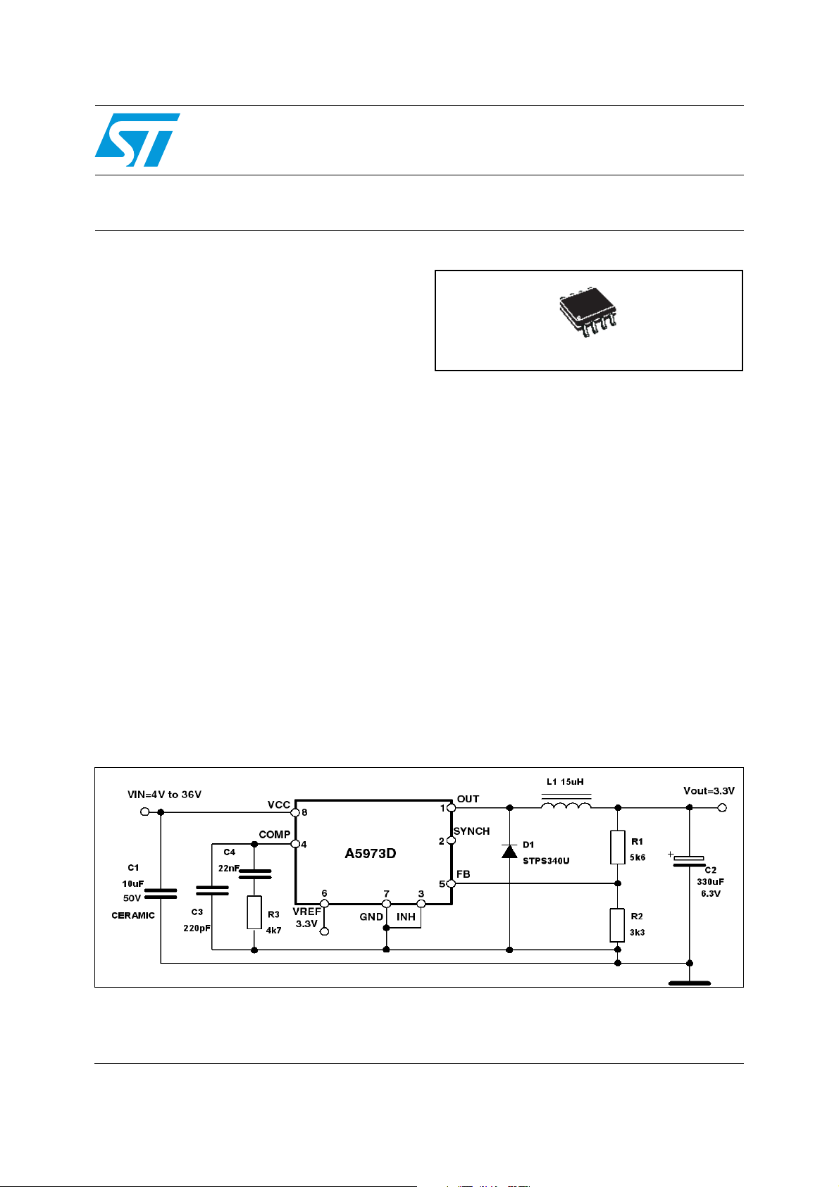
Figure 1. Application schematic
A5973D
for automotive applications
HSOP8 - exposed pad
Description
The A5973D is a step down monolithic power
switching regulator with a minimum switch current
limit of 2.25 A so it is able to deliver up to 2 A DC
current to the load depending on the application
conditions. The output voltage can be set from
1.235 V to 35 V. The high current level is also
achieved thanks to an HSOP8 package with
exposed frame, that allows to reduce the R
down to approximately 40 °C/W. The device uses
an internal p-channel DMOS transistor (with a
typical R
of 250 mΩ) as switching element
DS(on)
to minimize the size of the external components.
An internal oscillator fixes the switching frequency
at 250 kHz. Having a minimum input voltage of
4 V only it fits the automotive applications
requiring the device operation even in cold crank
conditions. Pulse by pulse current limit with the
internal frequency modulation offers an effective
constant current short circuit protection.
th(JA)
April 2009 Rev 6 1/41
www.st.com
41

Contents A5973D
Contents
1 Pin settings . . . . . . . . . . . . . . . . . . . . . . . . . . . . . . . . . . . . . . . . . . . . . . . . 4
1.1 Pin connection . . . . . . . . . . . . . . . . . . . . . . . . . . . . . . . . . . . . . . . . . . . . . . 4
1.2 Pin description . . . . . . . . . . . . . . . . . . . . . . . . . . . . . . . . . . . . . . . . . . . . . . 4
2 Electrical data . . . . . . . . . . . . . . . . . . . . . . . . . . . . . . . . . . . . . . . . . . . . . . 5
2.1 Maximum ratings . . . . . . . . . . . . . . . . . . . . . . . . . . . . . . . . . . . . . . . . . . . . 5
2.2 Thermal data . . . . . . . . . . . . . . . . . . . . . . . . . . . . . . . . . . . . . . . . . . . . . . . 5
3 Electrical characteristics . . . . . . . . . . . . . . . . . . . . . . . . . . . . . . . . . . . . . 6
4 Datasheet parameters over the temperature range . . . . . . . . . . . . . . . . 8
5 Functional description . . . . . . . . . . . . . . . . . . . . . . . . . . . . . . . . . . . . . . . 9
5.1 Power supply and voltage reference . . . . . . . . . . . . . . . . . . . . . . . . . . . . . 9
5.2 Voltages monitor . . . . . . . . . . . . . . . . . . . . . . . . . . . . . . . . . . . . . . . . . . . . 10
5.3 Oscillator and synchronization . . . . . . . . . . . . . . . . . . . . . . . . . . . . . . . . . 10
5.4 Current protection . . . . . . . . . . . . . . . . . . . . . . . . . . . . . . . . . . . . . . . . . . . 11
5.5 Error amplifier . . . . . . . . . . . . . . . . . . . . . . . . . . . . . . . . . . . . . . . . . . . . . . 12
5.6 PWM comparator and power stage . . . . . . . . . . . . . . . . . . . . . . . . . . . . . 12
5.7 Inhibit function . . . . . . . . . . . . . . . . . . . . . . . . . . . . . . . . . . . . . . . . . . . . . 13
5.8 Thermal shutdown . . . . . . . . . . . . . . . . . . . . . . . . . . . . . . . . . . . . . . . . . . 14
6 Additional features and protection . . . . . . . . . . . . . . . . . . . . . . . . . . . . 15
6.1 Feedback disconnection . . . . . . . . . . . . . . . . . . . . . . . . . . . . . . . . . . . . . . 15
6.2 Output overvoltage protection . . . . . . . . . . . . . . . . . . . . . . . . . . . . . . . . . 15
6.3 Zero load . . . . . . . . . . . . . . . . . . . . . . . . . . . . . . . . . . . . . . . . . . . . . . . . . 15
7 Closing the loop . . . . . . . . . . . . . . . . . . . . . . . . . . . . . . . . . . . . . . . . . . . 16
7.1 Error amplifier and compensation network . . . . . . . . . . . . . . . . . . . . . . . . 17
7.2 LC filter . . . . . . . . . . . . . . . . . . . . . . . . . . . . . . . . . . . . . . . . . . . . . . . . . . . 18
7.3 PWM comparator . . . . . . . . . . . . . . . . . . . . . . . . . . . . . . . . . . . . . . . . . . . 19
8 Application information . . . . . . . . . . . . . . . . . . . . . . . . . . . . . . . . . . . . . 21
2/41

A5973D Contents
8.1 Component selection . . . . . . . . . . . . . . . . . . . . . . . . . . . . . . . . . . . . . . . . 21
8.2 Layout considerations . . . . . . . . . . . . . . . . . . . . . . . . . . . . . . . . . . . . . . . . 24
8.3 Thermal considerations . . . . . . . . . . . . . . . . . . . . . . . . . . . . . . . . . . . . . . 24
8.4 Short-circuit protection . . . . . . . . . . . . . . . . . . . . . . . . . . . . . . . . . . . . . . . 26
8.5 Application circuit . . . . . . . . . . . . . . . . . . . . . . . . . . . . . . . . . . . . . . . . . . . 28
8.6 Positive buck-boost regulator . . . . . . . . . . . . . . . . . . . . . . . . . . . . . . . . . . 31
8.7 Negative buck-boost regulator . . . . . . . . . . . . . . . . . . . . . . . . . . . . . . . . . 32
8.8 Synchronization example . . . . . . . . . . . . . . . . . . . . . . . . . . . . . . . . . . . . . 33
8.9 Compensation network with MLCC at the output . . . . . . . . . . . . . . . . . . . 33
8.10 External SOFT_START network . . . . . . . . . . . . . . . . . . . . . . . . . . . . . . . . 35
9 Typical characteristics . . . . . . . . . . . . . . . . . . . . . . . . . . . . . . . . . . . . . . 36
10 Package mechanical data . . . . . . . . . . . . . . . . . . . . . . . . . . . . . . . . . . . . 38
11 Revision history . . . . . . . . . . . . . . . . . . . . . . . . . . . . . . . . . . . . . . . . . . . 40
3/41
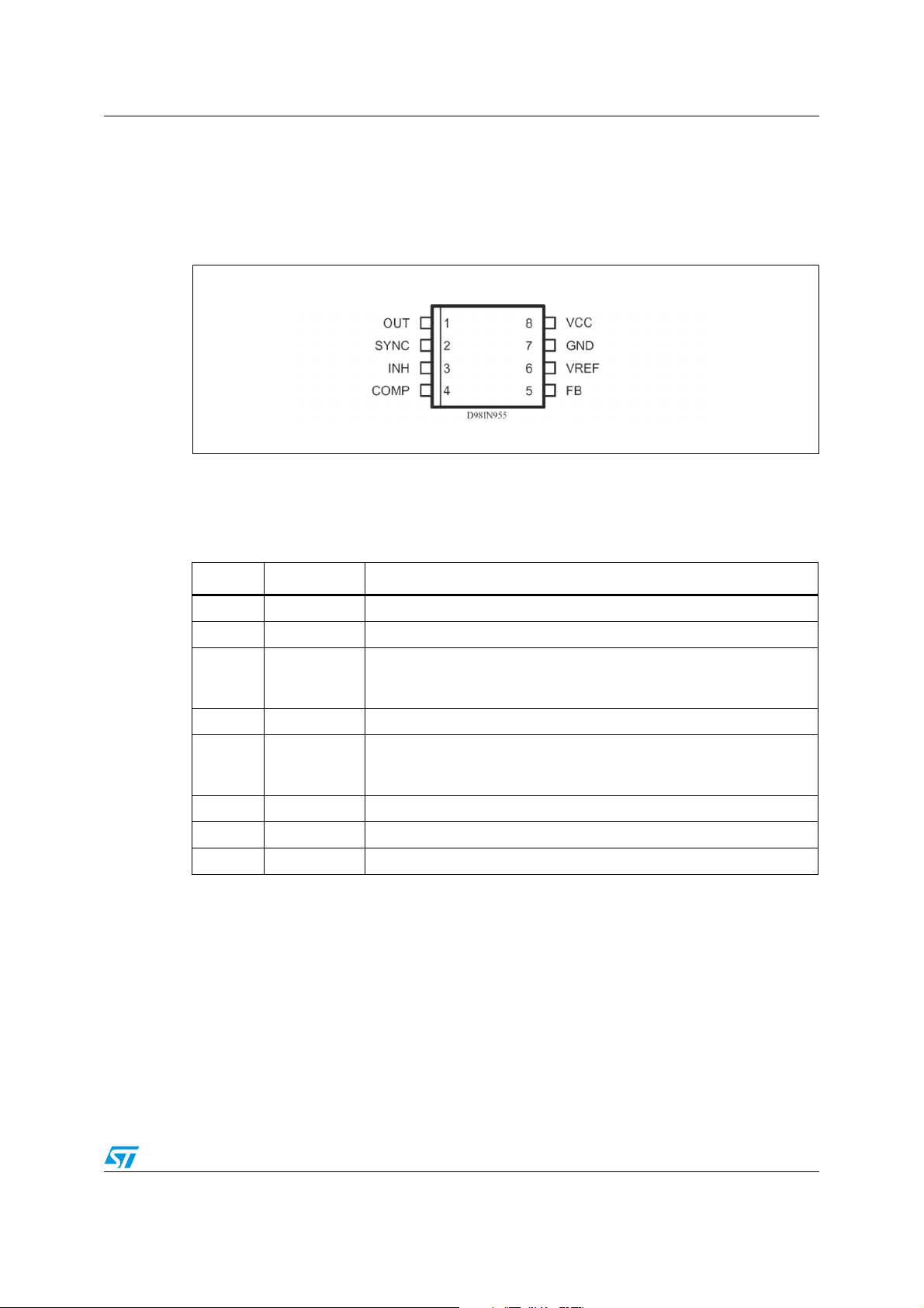
A5973D Pin settings
1 Pin settings
1.1 Pin connection
Figure 2. Pin connection (top view)
1.2 Pin description
Table 1. Pin description
N Pin Description
1 OUT Regulator output.
2 SYNCH Master/slave synchronization.
A logical signal (active high) disables the device. If INH not used the pin
3INH
4 COMP E/A output for frequency compensation.
5FB
6 VREF 3.3 V V
7 GND Ground.
8 VCC Unregulated DC input voltage.
must be grounded. When it is open an internal pull-up disable the
device.
Feedback input. Connecting directly to this pin results in an output
voltage of 1.23 V. An external resistive divider is required for higher
output voltages.
REF. No cap is requested for stability.
4/41
A5973D Electrical data
2 Electrical data
2.1 Maximum ratings
Table 2. Absolute maximum ratings
Symbol Parameter Value Unit
V
8
V
1
I
1
V
, V
4
V
3
V
2
P
TOT
T
J
T
STG
Input voltage 40 V
OUT pin DC voltage
OUT pin peak voltage at Δt = 0.1 μs
Maximum output current int. limit.
Analog pins 4 V
5
INH -0.3 to V
SYNCH -0.3 to 4 V
Power dissipation at T
Operating junction temperature range -40 to 150 °C
Storage temperature range -55 to 150 °C
2.2 Thermal data
Table 3. Thermal data
Symbol Parameter Value Unit
R
thJA
1. Package mounted on evaluation board
Maximum thermal resistance junction-ambient 40
-1 to 40
-5 to 40
CC
≤ 70 °C 2.25 W
A
(1)
V
V
V
°C/W
5/41
A5973D Electrical characteristics
3 Electrical characteristics
TJ = -40 °C to 125 °C, VCC = 12 V, unless otherwise specified.
Table 4. Electrical characteristics
Symbol Parameter Test condition Min Typ Max Unit
V
R
DS(on)
f
CC
I
SW
Operating input
voltage range
= 1.235 V; I0 = 2 A 4 36 V
V
0
MOSFET on
resistance
V
Maximum limiting
L
current
(1)
= 5 V 2.25 3 3.5
CC
= 5 V, TJ = 25 °C 2.533.5
V
CC
Switching frequency 212 250 280 kHz
Duty cycle 0 100 %
Dynamic characteristics (see test circuit)
V
Voltage feedback
5
h Efficiency V
4.4 V < V
20 mA < I0 < 2 A
= 5 V, V
0
DC characteristics
I
qop
I
I
qst-by
Total operating
quiescent current
Quiescent current Duty cycle = 0; V
q
V
Total stand-by
quiescent current
V
V
> 2.2 V 50 100 μA
inh
= 36 V;
C C
> 2.2 V
inh
Inhibit
0.250 0.5 W
< 36 V,
CC
= 12 V 90 %
CC
1.198 1.235 1.272 V
35mA
= 1.5 V 2.5 mA
FB
80 150 μA
A
INH threshold voltage
Device ON 0.8 V
Device OFF 2.2 V
Error amplifier
V
OH
V
OL
Io source Source output current V
I
o sink Sink output current V
I
gm Transconductance
High level output
voltage
Low level output
voltage
b Source bias current 2.5 4 μA
DC open loop gain R
V
= 1 V 3.5 V
FB
= 1.5 V 0.4 V
V
FB
= 1.9 V; VFB = 1 V 190 300 μA
COMP
= 1.9 V; V
COMP
L = ∞ 50 65 dB
I
= -0.1 mA to 0.1 mA;
COMP
V
= 1.9 V
COMP
= 1.5 V 1 1.5 mA
FB
2.3 mS
6/41
A5973D Electrical characteristics
Table 4. Electrical characteristics (continued)
Symbol Parameter Test condition Min Typ Max Unit
Synch function
High input voltage V
Low input voltage V
Slave synch current
Master output
amplitude
Output pulse width no load, V
Reference section
Reference voltage
Line regulation
Load regulation I
Short circuit current 5 18 35 mA
1. With TJ = 85 °C, I
2. Guaranteed by design
lim_min
= 4.4 to 36 V; 2.5 V
CC
= 4.4 to 36 V; 0.74 V
CC
V
= 0.74 V
synch
(2)
V
= 2.33 V
synch
I
= 3 mA 2.75 3 V
source
I
= 0 to 5 mA
REF
= 4.4 V to 36 V
V
CC
I
= 0 mA
REF
= 4.4 V to 36 V
V
CC
= 0 mA 8 15 mV
REF
= 2.5 A, assured by design, characterization and statistical correlation.
= 1.65 V 0.20 0.35 μs
synch
0.11
0.21
3.2 3.3 3.399 V
510mV
REF
0.25
0.45
V
mA
7/41

A5973D Datasheet parameters over the temperature range
4 Datasheet parameters over the temperature range
The 100% of the population in the production flow is tested at three different ambient
temperatures (-40 °C; +25 °C, +125 °C) to guarantee the datasheet parameters inside the
junction temperature range (-40 °C; +125 °C).
The device operation is so guaranteed when the junction temperature is inside the (-40 °C;
+150 °C) temperature range. The designer can estimate the silicon temperature increase
respect to the ambient temperature evaluating the internal power losses generated during
the device operation (please refer to the Chapter 2.2).
However the embedded thermal protection disables the switching activity to protect the
device in case the junction temperature reaches the T
temperature.
All the datasheet parameters can be guaranteed to a maximum junction temperature of
+125 °C to avoid triggering the thermal shutdown protection during the testing phase
because of self heating.
SHTDWN
(+150 °C±10 °C)
8/41
A5973D Functional description
5 Functional description
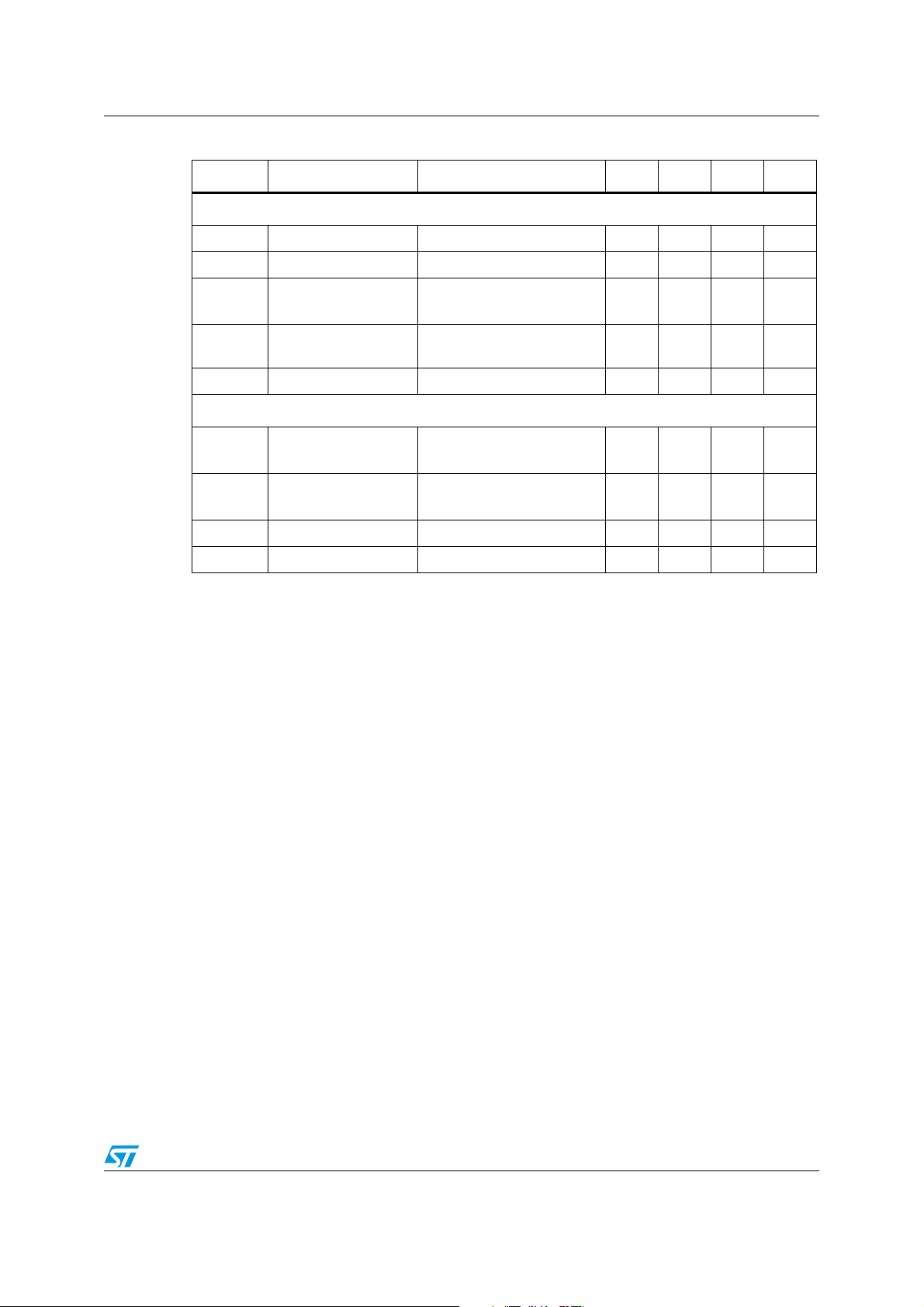
The main internal blocks are shown in the device block diagram in Figure 3. They are:
● A voltage regulator supplying the internal circuitry. From this regulator, a 3.3 V
reference voltage is externally available.
● A voltage monitor circuit which checks the input and the internal voltages.
● A fully integrated sawtooth oscillator with a frequency of 250 kHz ± 15 %, including also
the voltage feed forward function and an input/output synchronization pin.
● Two embedded current limitation circuits which control the current that flows through
the power switch. The pulse-by-pulse current limit forces the power switch OFF cycle
by cycle if the current reaches an internal threshold, while the frequency shifter reduces
the switching frequency in order to significantly reduce the duty cycle.
● A transconductance error amplifier.
● A pulse width modulator (PWM) comparator and the relative logic circuitry necessary to
drive the internal power.
● A high side driver for the internal P-MOS switch.
● An inhibit block for stand-by operation.
● A circuit to implement the thermal protection function.
Figure 3. Block diagram
5.1 Power supply and voltage reference
The internal regulator circuit (shown in Figure 4) consists of a start-up circuit, an internal
voltage pre-regulator, the Bandgap voltage reference and the Bias block that provides
current to all the blocks. The Starter supplies the start-up currents to the entire device when
the input voltage goes high and the device is enabled (inhibit pin connected to ground). The
pre-regulator block supplies the Bandgap cell with a pre-regulated voltage V
very low supply voltage noise sensitivity.
that has a
REG
9/41
A5973D Functional description
5.2 Voltages monitor
An internal block continuously senses the Vcc, V
their thresholds, the regulator begins operating. There is also a hysteresis on the V
(UVLO).
Figure 4. Internal circuit
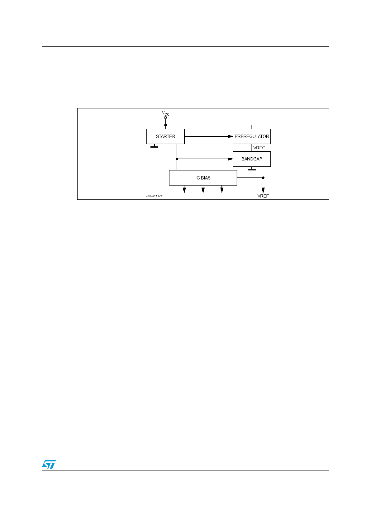
5.3 Oscillator and synchronization
Figure 5 shows the block diagram of the oscillator circuit.
The clock generator provides the switching frequency of the device, which is internally fixed
at 250 kHz. The frequency shifter block acts to reduce the switching frequency in case of
strong overcurrent or short circuit. The clock signal is then used in the internal logic circuitry
and is the input of the ramp generator and synchronizer blocks.
and Vbg. If the voltages go higher than
ref
CC
The ramp generator circuit provides the sawtooth signal, used for PWM control and the
internal voltage feed-forward, while the synchronizer circuit generates the synchronization
signal. The device also has a synchronization pin which can work both as master and slave.
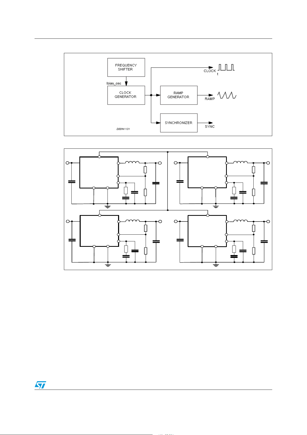
Beating frequency noise is an issue when more than one voltage rail is on the same board.
A simple way to avoid this issue is to operate all the regulators at the same switching
frequency.
The synchronization feature of a set of the A5973D is simply get connecting together their
SYNCH pin. The device with highest switching frequency will be the MASTER and it
provides the synchronization signal to the others. Therefore the SYNCH is a I/O pin to
deliver or recognize a frequency signal. The synchronization circuitry is powered by the
internal reference (V
) so a small filtering capacitor (≥ 100 nF) connected between V
REF
REF
pin and the signal ground of the Master device is suggested for its proper operation.
However when a set of synchronized devices populates a board it is not possible to know in
advance the one working as Master, so the filtering capacitor have to be designed for whole
set of devices.
When one or more devices are synchronized to an external signal, its amplitude have to be
in comply with specifications given in the Tab l e 4 . The frequency of the synchronization
signal must be, at a minimum, higher than the maximum guaranteed natural switching
frequency of the device (275 kHz, see Tab le 4 ) while the duty cycle of the synchronization
signal can vary from approximately 10% to 90%. The small capacitor under V
REF
pin is
required for this operation.
10/41
A5973D Functional description
Figure 5. Oscillator circuit block diagram
Figure 6. Synchronization example
OUT
OUT
SYNCH
SYNCH
SYNCH
A5973D
A5973D
A5973D
OUT
OUT
OUT
FB
FB
FB
COMP
COMP
COMP
SYNCH
SYNCH
SYNCH
A5973D
A5973D
A5973D
OUT
FB
FB
FB
COMP
COMP
COMP
SS/INH
SS/INH
SS/INH
SYNCH
SYNCH
SYNCH
A5973D
A5973D
A5973D
SS/INH
SS/INH
SS/INH
GND
GND
GND
GND
GND
GND
OUT
OUT
OUT
FB
FB
FB
COMP
COMP
COMP
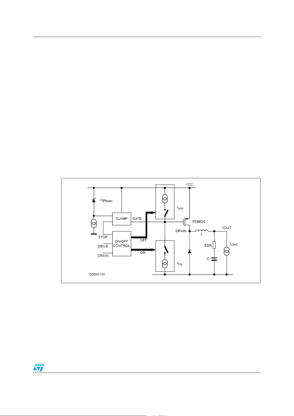
5.4 Current protection
The A5973D features two types of current limit protection: pulse-by-pulse and frequency
foldback.
The schematic of the current limitation circuitry for the pulse-by-pulse protection is shown in
Figure 7. The output power PDMOS transistor is split into two parallel PDMOS transistors.
The smallest one includes a resistor in series, R
R
switched off until the next falling edge of the internal clock pulse. Due to this reduction of the
ON time, the output voltage decreases. Since the minimum switch ON time necessary to
sense the current in order to avoid a false overcurrent signal is too short to obtain a
sufficiently low duty cycle at 250 kHz (see Chapter 8.4), the output current in strong
overcurrent or short circuit conditions could be not properly limited. For this reason the
switching frequency is also reduced, thus keeping the inductor current under its maximum
and if it reaches the threshold, the mirror becomes unbalanced and the PDMOS is
SENSE
SS/INH
SS/INH
SS/INH
SYNCH
SYNCH
SYNCH
A5973D
A5973D
A5973D
SS/INH
SS/INH
SS/INH
. The current is sensed through
SENSE
GND
GND
GND
GND
GND
GND
OUT
OUT
OUT
FB
FB
FB
COMP
COMP
COMP
11/41
A5973D Functional description
threshold. The frequency shifter (Figure 5) functions based on the feedback voltage. As the
feedback voltage decreases (due to the reduced duty cycle), the switching frequency
decreases also.
Figure 7. Current limitation circuitry
5.5 Error amplifier
The voltage error amplifier is the core of the loop regulation. It is a transconductance
operational amplifier whose non inverting input is connected to the internal voltage
reference (1.235 V), while the inverting input (FB) is connected to the external divider or
directly to the output voltage. The output (COMP) is connected to the external compensation
network. The uncompensated error amplifier has the following characteristics:
Table 5. Uncompensated error amplifier characteristics
Description Values
Transconductance 2300 µS
Low frequency gain 65 dB
Minimum sink/source voltage 1500 µA/300 µA
Output voltage swing 0.4 V/3.65 V
Input bias current 2.5 µA
The error amplifier output is compared to the oscillator sawtooth to perform PWM control.
5.6 PWM comparator and power stage
This block compares the oscillator sawtooth and the error amplifier output signals to
generate the PWM signal for the driving stage.
The power stage is a highly critical block, as it functions to guarantee a correct turn ON and
turn OFF of the PDMOS. The turn ON of the power element, or more accurately, the rise
time of the current at turn ON, is a very critical parameter. At a first approach, it appears that
the faster the rise time, the lower the turn ON losses.
However, there is a limit introduced by the recovery time of the recirculation diode.
12/41
A5973D Functional description
In fact, when the current of the power element is equal to the inductor current, the diode
turns OFF and the drain of the power is able to go high. But during its recovery time, the
diode can be considered a high value capacitor and this produces a very high peak current,
responsible for numerous problems:
● Spikes on the device supply voltage that cause oscillations (and thus noise) due to the
board parasites.
● Turn ON overcurrent leads to a decrease in the efficiency and system reliability.
● Major EMI problems.
● Shorter freewheeling diode life.
The fall time of the current during turn OFF is also critical, as it produces voltage spikes (due
to the parasites elements of the board) that increase the voltage drop across the PDMOS.
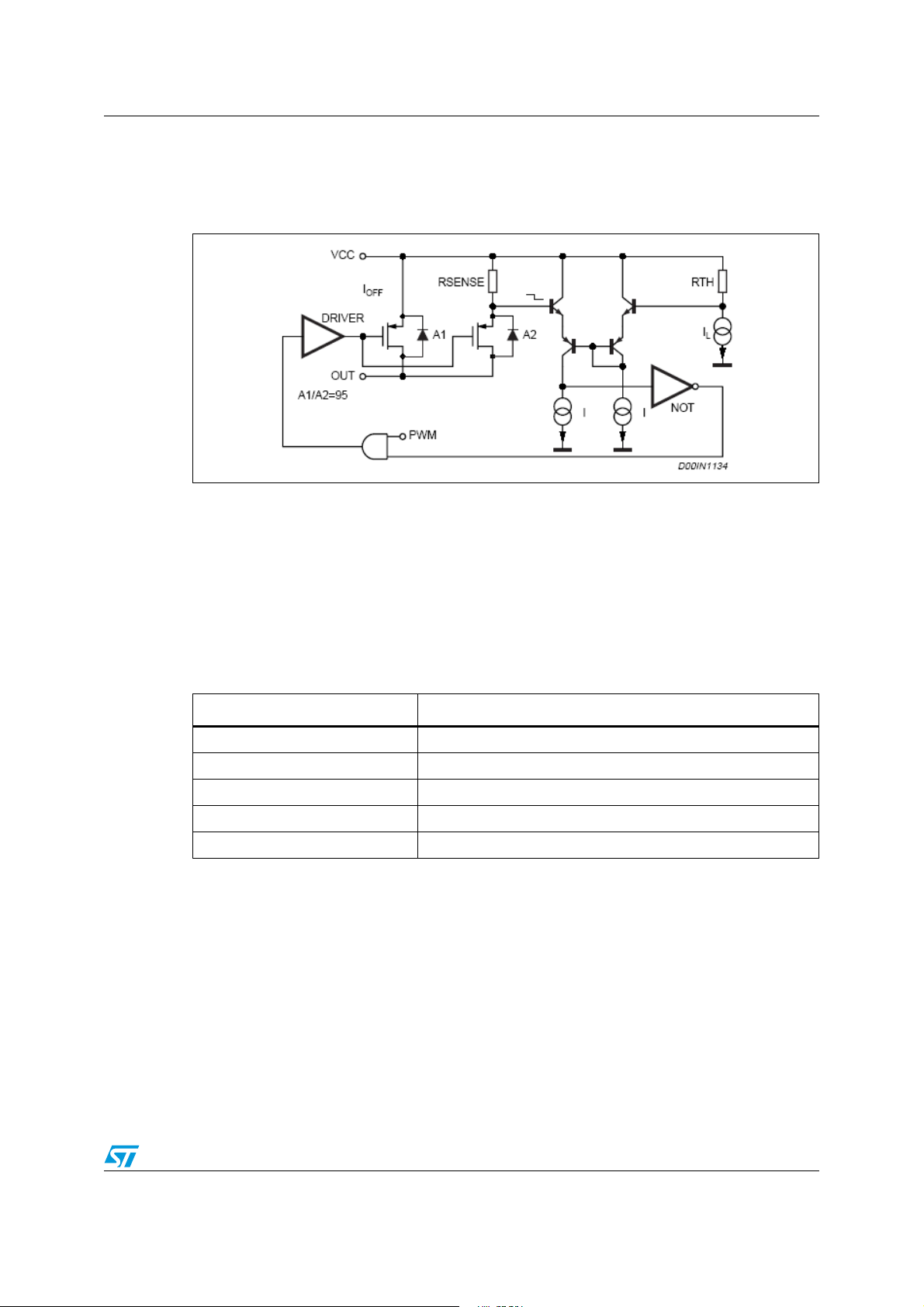
In order to minimize these problems, a new driving circuit topology has been used and the
block diagram is shown in Figure 8. The basic idea is to change the current levels used to
turn the power switch ON and OFF, based on the PDMOS and the gate clamp status.
This circuitry allows the power switch to be turned OFF and ON quickly and addresses the
freewheeling diode recovery time problem. The gate clamp is necessary to ensure that V
of the internal switch does not go higher than V
max. The ON/OFF Control block protects
GS
GS
against any cross conduction between the supply line and ground.
Figure 8. Driving circuitry
5.7 Inhibit function
The inhibit feature is used to put the device in standby mode. With the INH pin higher than
2.2 V the device is disabled and the power consumption is reduced to less than 100 µA.
With the INH pin lower than 0.8 V, the device is enabled. If the INH pin is left floating, an
internal pull up ensures that the voltage at the pin reaches the inhibit threshold and the
device is disabled. The pin is also V
compatible.
cc
13/41

A5973D Functional description
5.8 Thermal shutdown
The shutdown block generates a signal that turns OFF the power stage if the temperature of
the chip goes higher than a fixed internal threshold (150±10 °C). The sensing element of the
chip is very close to the PDMOS area, ensuring fast and accurate temperature detection. A
hysteresis of approximately 20 °C keeps the device from turning ON and OFF continuously.
14/41

A5973D Additional features and protection
6 Additional features and protection
6.1 Feedback disconnection
If the feedback is disconnected, the duty cycle increases towards the maximum allowed
value, bringing the output voltage close to the input supply. This condition could destroy the
load.
To avoid this hazardous condition, the device is turned OFF if the feedback pin is left
floating.
6.2 Output overvoltage protection
Overvoltage protection, or OVP, is achieved by using an internal comparator connected to
the feedback, which turns OFF the power stage when the OVP threshold is reached. This
threshold is typically 30% higher than the feedback voltage.
When a voltage divider is required to adjust the output voltage (Figure 15), the OVP
intervention will be set at:
Equation 1
Where R
R
is between the feedback pin and ground.
2
is the resistor connected between the output voltage and the feedback pin, and
1
6.3 Zero load
Due to the fact that the internal power is a PDMOS, no boostrap capacitor is required and so
the device works properly even with no load at the output. In this case it works in burst
mode, with a random burst repetition rate.
V
OVP
R1R2+
--------------------
1.3
• V
•=
R
FB
2
15/41

A5973D Closing the loop
7 Closing the loop
Figure 9. Block diagram of the loop
16/41

A5973D Closing the loop
7.1 Error amplifier and compensation network
The output L-C filter of a step-down converter contributes with 180 degrees phase shift in
the control loop. For this reason a compensation network between the COMP pin and
GROUND is added. The simplest compensation network together with the equivalent circuit
of the error amplifier are shown in Figure 10. R
open loop gain. CP does not significantly affect system stability but it is useful to reduce the
noise of the COMP pin.
The transfer function of the error amplifier and its compensation network is:
Equation 2
A
A0s()
---------------------------------------------------------------------------------------------------------------------------------------------------------------------------------------------------=
2
s
R0• C0Cp+()RcCcsR0Cc• R0C0Cp+()RcCc•+•+()1+•+•••
V0
and CC introduce a pole and a zero in the
C
1s+ RcCc••()•
Where A
= Gm · R
vo
o
Figure 10. Error amplifier equivalent circuit and compensation network
The poles of this transfer function are (if C
>> C0+CP):
c
Equation 3
Equation 4
P1
------------------------------------------------------- -=
F
P2
2 π• R
17/41
• Cc•
2 π• R
1
• C0Cp+()•
c
0
1
-------------------------------------=
F

A5973D Closing the loop
whereas the zero is defined as:
Equation 5
F
is the low frequency which sets the bandwidth, while the zero FZ1 is usually put near to
P1
the frequency of the double pole of the L-C filter (see below). F
frequency.
7.2 LC filter
The transfer function of the L-C filter is given by:
Equation 6
ALCs()
where R
If R
Equation 7
LOAD
>>ESR, the previous expression of ALC can be simplified and becomes:
LOAD
F
-------------------------------------=
Z1
2 π• Rc• Cc•
R
----------------------------------------------------------------------------------------------------------------------------------------------------------------------------------------------------=
s
2
LC
OUT
LOAD
ESR R
+()s ESR C
LOAD
is defined as the ratio between V
A
s()
LC
----------------------------------------------------------------------------------------------=
LC
1 ESR C
• s2ESR C
OUT
1
1 ESR C
and I
OUT
• s•+
OUT
• s1+•+•
P2
s••+()•
OUT
• R
OUT
.
OUT
OUT
is usually at a very high
L+•()R
LOAD
+•+•••
LOAD
The zero of this transfer function is given by:
Equation 8
--------------------------------------------------- -=
F
O
2 π• ESR• C
is the zero introduced by the ESR of the output capacitor and it is very important to
F
0
1
•
OUT
increase the phase margin of the loop.
The poles of the transfer function can be calculated through the following expression:
Equation 9
F
PLC1 2,
In the denominator of A
ESR C
--------------------------------- ---------------------------------------------------------- -----------------------------------------------=
the typical second order system equation can be recognized:
LC
OUT
ESR C
•()
2L• C
•
OUT
OUT
2
4L• C
•–±•–
OUT
Equation 10
s22 δ•ω
• s ω
n
2
+•+
n
18/41

A5973D Closing the loop
If the damping coefficient δ is very close to zero, the roots of the equation become a double
root whose value is ω
Similarly for A
LC
.
n
the poles can usually be defined as a double pole whose value is:
Equation 11
F
PLC
----------------------------------------------=
2 π• LC
1
••
OUT
7.3 PWM comparator
The PWM gain is given by the following formula:
Equation 12
V
G
PWM
s()
-------------------------------------------------------------=
V
OSCMAXVOSCMIN
cc
–()
where V
OSCMAX
is the maximum value of a sawtooth waveform and V
OSCMIN
is the
minimum value. A voltage feed forward is implemented to ensure a constant GPWM. This is
obtained by generating a sawtooth waveform directly proportional to the input voltage V
CC
.
Equation 13
V
OSCMAXVOSCMIN
– KV
•=
CC
Where K is equal to 0.076. Therefore the PWM gain is also equal to:
Equation 14
s()
1
--- - const==
K
G
PWM
This means that even if the input voltage changes, the error amplifier does not change its
value to keep the loop in regulation, thus ensuring a better line regulation and line transient
response.
In summary, the open loop gain can be expressed as:
Equation 15
R
2
--------------------
• A
Gs() G
PWM
s()
R1R2+
s()• ALC• s()=
O
19/41

A5973D Closing the loop
Example:
Considering R
F
= 9 Hz
P1
F
= 256 kHz
P2
F
= 2.68 kHz
Z1
If L = 22 µH, C
F
PLC
F
= 19.89 kHz
0
Finally R
= 2.7 kΩ, CC = 22 nF and CP = 220 pF, the poles and zeroes of A0 are:
C
= 100 µF and ESR = 80 mΩ, the poles and zeroes of ALC become:
OUT
= 3.39 kHz
= 5.6 kΩ and R2 = 3.3 kΩ.
1
The gain and phase bode diagrams are plotted respectively in Figure 11 and Figure 12.
Figure 11. Module plot
Figure 12. Phase plot
The cut-off frequency and the phase margin are:
Equation 16
FC22.8K Hz=
Phase margin = 39.8°
20/41

A5973D Application information
8 Application information
8.1 Component selection
● Input capacitor
The input capacitor must be able to support the maximum input operating voltage and the
maximum RMS input current.
Since step-down converters draw current from the input in pulses, the input current is
squared and the height of each pulse is equal to the output current. The input capacitor has
to absorb all this switching current, which can be up to the load current divided by two (worst
case, with duty cycle of 50 %). For this reason, the quality of these capacitors has to be very
high to minimize the power dissipation generated by the internal ESR, thereby improving
system reliability and efficiency. The critical parameter is usually the RMS current rating,
which must be higher than the RMS input current. The maximum RMS input current (flowing
through the input capacitor) is:
Equation 17
2
I
RMSIO
D
2D
•
--------------- -–
η
2
D
------ -+•=
2
η
Where η is the expected system efficiency, D is the duty cycle and I
is the output DC
O
current. This function reaches its maximum value at D = 0.5 and the equivalent RMS current
is equal to I
divided by 2 (considering η = 1). The maximum and minimum duty cycles are:
O
Equation 18
V
+
D
MAX
OUTVF
------------------------------------ -=
V
–
INMINVSW
and
Equation 19
V
+
OUTVF
MIN
--------------------------------------=
V
–
INMAXVSW
D
21/41
A5973D Application information
Where VF is the freewheeling diode forward voltage and VSW the voltage drop across the
internal PDMOS. Considering the range D
MIN
to D
, it is possible to determine the max
MAX
IRMS going through the input capacitor. Capacitors that can be considered are:
Electrolytic capacitors:
These are widely used due to their low price and their availability in a wide range of
RMS current ratings.
The only drawback is that, considering ripple current rating requirements, they are
physically larger than other capacitors.
Ceramic capacitors:
If available for the required value and voltage rating, these capacitors usually have a
higher RMS current rating for a given physical dimension (due to very low ESR).
The drawback is the considerably high cost.
Tantalum capacitors:
Very good, small tantalum capacitors with very low ESR are becoming more available.
However, they can occasionally burn if subjected to very high current during charge.
Therefore, it is better to avoid this type of capacitor for the input filter of the device. They
can, however, be subjected to high surge current when connected to the power supply.
Table 6. List of ceramic capacitors for the A5973D
Manufacturer Series Capacitor value (µ) Rated voltage (V)
TAIYO YUDEN UMK325BJ106MM-T 10 50
MURATA GRM42-2 X7R 475K 50 4.7 50
● Output capacitor
The output capacitor is very important to meet the output voltage ripple requirement.
Using a small inductor value is useful to reduce the size of the choke but it increases the
current ripple. So, to reduce the output voltage ripple, a low ESR capacitor is required.
Nevertheless, the ESR of the output capacitor introduces a zero in the open loop gain,
which helps to increase the phase margin of the system. If the zero goes to a very high
frequency, its effect is negligible. For this reason, ceramic capacitors and very low ESR
capacitors in general should be avoided.
Tantalum and electrolytic capacitors are usually a good choice for this purpose. A list of
some tantalum capacitor manufacturers is provided in Table 7.: Output capacitor selection.
22/41
A5973D Application information
Table 7. Output capacitor selection
Manufacturer Series Cap value (µF) Rated voltage (V) ESR (mΩ)
Sanyo POSCAP
AVX TPS 100 to 470 4 to 35 50 to 200
KEMET T494/5 100 to 470 4 to 20 30 to 200
Sprague 595D 220 to 390 4 to 20 160 to 650
1. POSCAP capacitors have some characteristics which are very similar to tantalum.
● Inductor
(1)
TAE 100 to 470 4 to 16 25 to 35
THB/C/E 100 to 470 4 to 16 25 to 55
The inductor value is very important as it fixes the ripple current flowing through the output
capacitor. The ripple current is usually fixed at 20 - 40% of I
I
max = 2 A. The approximate inductor value is obtained using the following formula:
O
, which is 0.4 - 0.8 A with
omax
Equation 20
–()
V
INVOUT
----------------------------------
L
ΔI
•=
T
ON
where T
V
OUT
is the ON time of the internal switch, given by D · T. For example, with
ON
= 3.3 V, V
= 2 V and ΔIO = 0.6 A, the inductor value is about 17 µH. The peak current
IN
through the inductor is given by:
Equation 21
ΔI
I
PKIO
-----+=
2
and it can be observed that if the inductor value decreases, the peak current (which must be
lower than the current limit of the device) increases. So, when the peak current is fixed, a
higher inductor value allows a higher value for the output current. In the Table 8.: Inductor
selection, some inductor manufacturers are listed.
Table 8. Inductor selection
Manufacturer Series Inductor value (µH) Saturation current (A)
Coilcraft DO3316T 15 to 33 2.0 to 3.0
Coiltronics UP1B 22 to 33 2.0 to 2.4
BI HM76-3 15 to 33 2.5 to 3.3
Epcos B82476 15 to 33 2 to 3
Wurth Elektronik 74456115 15 to 33 2.5 to 3
23/41
A5973D Application information
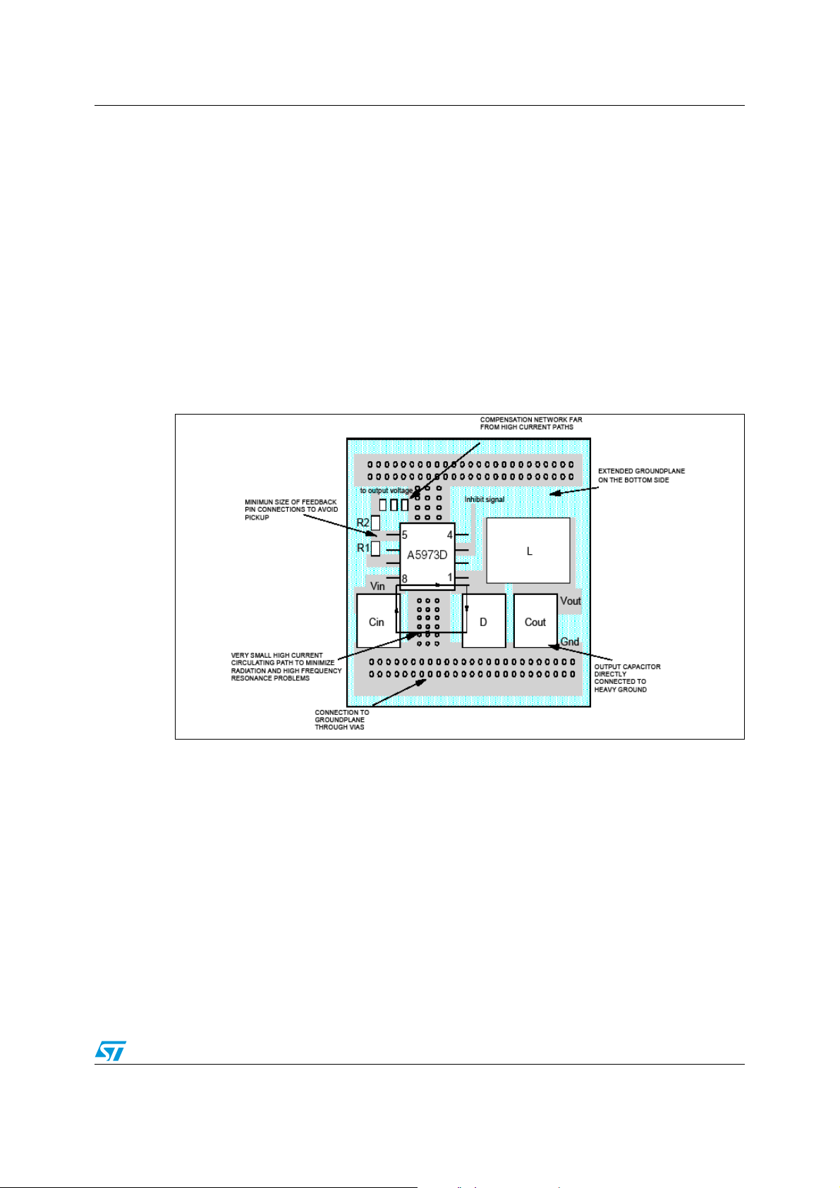
8.2 Layout considerations
The layout of switching DC-DC converters is very important to minimize noise and
interference. Power-generating portions of the layout are the main cause of noise and so
high switching current loop areas should be kept as small as possible and lead lengths as
short as possible.
High impedance paths (in particular the feedback connections) are susceptible to
interference, so they should be as far as possible from the high current paths. An layout
example is provided in Figure 13 below.
The input and output loops are minimized to avoid radiation and high frequency resonance
problems. The feedback pin connections to the external divider are very close to the device
to avoid pick-up noise. Another important issue is the ground plane of the board. Since the
package has an exposed pad, it is very important to connect it to an extended ground plane
in order to reduce the thermal resistance junction-to-ambient.
Figure 13. Layout example
8.3 Thermal considerations
The dissipated power of the device is tied to three different sources:
● Conduction losses due to the not insignificant R
Equation 22
P
ON
Where D is the duty cycle of the application. Note that the duty cycle is theoretically given by
the ratio between V
and VIN, but in practice it is substantially higher than this value to
OUT
, which are equal to:
DSON
R
DSONIOUT
24/41
2
()•
D•=
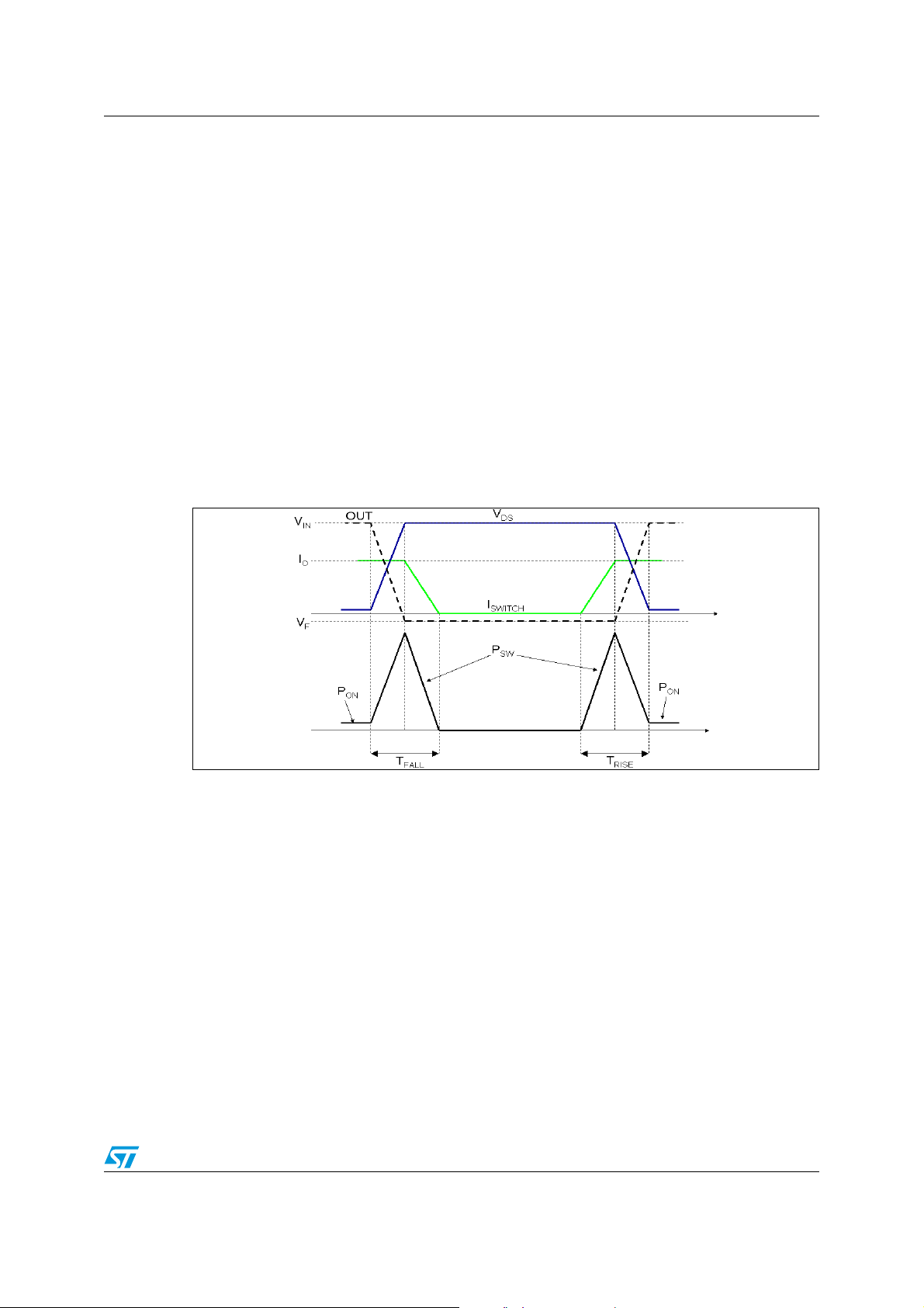
A5973D Application information
compensate for the losses in the overall application. For this reason, the switching losses
related to the R
● Switching losses due to turning ON and OFF. These are derived using the following
increases compared to an ideal case.
DSON
equation:
Equation 23
T
+()
ONTOFF
----------------------------------- -
P
SWVINIOUT
•• F
2
=• I
SWVIN
• FSW••=
OUTTSW
Where T
RISE
and T
represent the switching times of the power element that cause the
FAL L
switching losses when driving an inductive load (see Figure 14). T
switching time.
Figure 14. Switching losses
● Quiescent current losses.
Equation 24
is the equivalent
SW
Where I
Example:
–V
–V
–I
is the quiescent current.
Q
= 12 V
IN
= 3.3 V
OUT
= 2 A
OUT
P
VINIQ•=
Q
25/41

A5973D Application information
R
has a typical value of 0.25 @ 25 °C and increases up to a maximum value of 0.5. @
DS(on)
150 °C. We can consider a value of 0.4 Ω.
T
is approximately 70 ns.
SW
I
has a typical value of 2.5 mA @ VIN = 12 V.
Q
The overall losses are:
Equation 25
P
TOTRDSONIOUT
2
• 0.3 12 2• 70• 109–• 250• 103–12 2.5• 103–•+•+• 0.93W≅=
0.4 2
2
()•
DVINI
• TSW• F
OUT
SWVINIQ
=•+•+•=
The junction temperature of device will be:
Equation 26
Where T
TJTARth
is the ambient temperature and Rth
A
P
•+=
JA–
J-A
TOT
is the thermal resistance junction-toambient. Considering that the device is mounted on board with a good ground plane, that it
has a thermal resistance junction-to-ambient (Rth
) of about 42 °C/W, and an ambient
J-A
temperature of about 70 °C:
Equation 27
TJ70 0.93 42 110°C≅•+=
8.4 Short-circuit protection
In overcurrent protection mode, when the peak current reaches the current limit, the device
reduces the T
frequency to approximately one third of its nominal value even when synchronized to an
external signal (see Section 5.4: Current protection). In these conditions, the duty cycle is
strongly reduced and, in most applications, this is enough to limit the current to ILIM. In any
event, in case of heavy short-circuit at the output (V
application conditions (V
peak could reach values higher than ILIM. This can be understood considering the inductor
current ripple during the ON and OFF phases:
● ON phase
Equation 28
● OFF phase
Equation 29
where V
is the voltage drop across the diode, DCRL is the series resistance of the inductor.
D
down to its minimum value (approximately 250 nsec) and the switching
ON
value and parasitic effect of external components) the current
cc
I
Δ
L TON
Δ
I
L TOFF
= 0 V) and depending on the
O
VINV
– DCRLR
out
------------------------------------------------------------------------------------
V
DVout
---------------------------------------------------------------
+()I⋅–
DSON
L
DCRLI•++()–
L
()=
T
()=
OFF
T
ON
26/41

A5973D Application information
In short-circuit conditions V
is negligible so during T
OUT
the voltage across the inductor
OFF
is very small as equal to the voltage drop across parasitic components (typically the DCR of
the inductor and the V
the inductor is instead maximized as approximately equal to V
of the free wheeling diode) while during TON the voltage applied
FW
.
IN
So the Equation 28 and the Equation 29 in overcurrent conditions can be simplified to:
Equation 30
considering T
VINDCRLR
I
Δ
L TON
that has been already reduced to its minimum.
ON
----------------------------------------------------------------
+()I⋅–
DSON
L
T
()
ON MIN
V
-------- -
L
IN
250ns()≅=
Equation 31
I
Δ
L TOFF
considering that f
V
DVout
---------------------------------------------------------------
has been already reduced to one third of the nominal.
SW
DCRLI•++()–
L
3T⋅
()
SW
In case a short circuit at the output is applied and V
V
DVout
---------------------------------------------------------------
= 12 V the inductor current is
IN
DCRLI•++()–
L
12μ s()≅=
controlled in most of the applications (see Figure 15). When the application must sustain the
short-circuit condition for an extended period, the external components (mainly the inductor
and diode) must be selected based on this value.
In case the V
does not compensate the current increase during T
an example of a power up phase with V
is very high, it could occur that the ripple current during T
IN
= V
IN
IN MAX
(Equation 30). The Figure 17 shows
ON
= 36 V where Δ
IL TON
(Equation 31)
OFF
> Δ
IL TOFF
so the
current escalates and the balance between Equation 30 and Equation 31 occurs at a current
slightly higher than the current limit. This must be taken into account in particular to avoid
the risk of an abrupt inductor saturation.
Figure 15. Short-circuit current V
= 12 V
IN
27/41

A5973D Application information
Figure 16. Short-circuit current VIN = 24 V
Figure 17. Short-circuit current V
8.5 Application circuit
Figure 18 shows the evaluation board application circuit, where the input supply voltage,
V
, can range from 4 V to 36 V and the output voltage is adjustable from 1.235 V to 6.3 V
CC
due to the voltage rating of the output capacitor,.
= 36 V
IN
28/41

A5973D Application information
Figure 18. Evaluation board application circuit
Table 9. Component list
Reference Part number Description Manufacturer
C1 GRM42-2 X7R 475K 50 4.7 µF, 50 V Murata
C2 POSCAP 6TAE330ML 330 µF, 6.3 V Sanyo
C3 C1206C221J5GAC 47 pF, 5%, 50 V KEMET
C4 C1206C223K5RAC 22 nF, 10%, 50 V KEMET
R1 5.6 kΩ, 1%, 0.1 W 0603 Neohm
R2 3.3 kΩ, 1%, 0.1 W 0603 Neohm
R3 22 kΩ, 1%, 0.1 W 0603 Neohm
D1 STPS3L40U 2 A, 40 V STMicroelectronics
L1 DO3316T-153MLD 15 µH, 3.1 A Coilcraft
29/41

A5973D Application information
Figure 19. PCB layout (component side)
Figure 20. PCB layout (bottom side)
Figure 21. PCB layout (front side)
LS
LC
30/41

A5973D Application information
8.6 Positive buck-boost regulator
The device can be used to implement a step-up/down converter with a positive output
voltage.
The output voltage is given by:
Equation 32
D
-------------
V
OUT
where the ideal duty cycle D for the buck boost converter is:
Equation 33
D
However, due to power losses in the passive elements, the real duty cycle is always higher
than this. The real value (that can be measured in the application) should be used in the
following formulas.
The peak current flowing in the embedded switch is:
V
IN
V
OUT
----------------------------- -=
VINV
+
⋅=
1D–
OUT
Equation 34
I
SW
I
LOAD
---------------
1D–
I
RIPPLE
------------------- -+
2
I
LOAD
---------------
1D–
V
IN
---------- -
2L⋅
---------
⋅+==
f
SW
D
while its average current is equal to:
Equation 35
I
LOAD
---------------=
I
SW
1D–
This is due to the fact that the current flowing through the internal power switch is delivered
to the output only during the OFF phase.
The switch peak current must be lower than the minimum current limit of the overcurrent
protection (see Ta bl e 4 for details) while the average current must be lower than the rated
DC current of the device.
As a consequence, the maximum output current is:
Equation 36
where I
SW MAX
I
OUT MAXISW MAX
represents the rated current of the device.
1D–()⋅≅
The current capability is reduced by the term (1-D) and so, for example, with a duty cycle of
0.5, and considering an average current through the switch of 2 A, the maximum output
current deliverable to the load is 1 A.
The figure below shows the schematic circuit of this topology for a 12 V output voltage and
5 V input.
31/41

A5973D Application information
Figure 22. Positive buck-boost regulator
8.7 Negative buck-boost regulator
In Figure 23, the schematic circuit for a standard buck-boost topology is shown. The output
voltage is:
Equation 37
D
V
OUT
-------------
VIN–
⋅=
1D–
where the ideal duty cycle D for the buck boost converter is:
Equation 38
V–
OUT
----------------------------- -=
D
VINV
–
OUT
The considerations given in Section 8.7 for the real duty cycle are still valid here.
Also the Equation 34 till Equation 36 can be used to calculate the maximum output current.
So, as an example, considering the conversion V
= 12 V to V
IN
OUT
= -5 V, I
LOAD
= 0.5 A:
Equation 39
D
5
--------------- - 0.706==
512+
Equation 40
I
SW
I
LOAD
---------------
1D–
0.5
----------------------- - 1.7A== =
10.706–
An important thing to take into account is that the ground pin of the device is connected to
the negative output voltage. Therefore, the device is subjected to a voltage equal to V
IN-VO
which must be lower than 36 V (the maximum operating input voltage).
,
32/41
A5973D Application information
Figure 23. Negative buck-boost regulator
8.8 Synchronization example
See Chapter 5.3 for details.
Figure 24. Synchronization example
8.9 Compensation network with MLCC at the output
MLCCs (multiple layer ceramic capacitor) with values in the range of 10 µF-22 µF and rated
voltages in the range of 10 V-25 V are available today at relatively low cost from many
manufacturers.
These capacitors have very low ESR values (a few mΩ) and thus are occasionally used for
the output filter in order to reduce the voltage ripple and the overall size of the application.
However, a very low ESR value affects the compensation of the loop (see Section 7) and in
order to keep the system stable, a more complicated compensation network may be
required. However, due to the architecture of the internal error amplifier the bandwidth with
this compensation is limited.
That is why output capacitors with a not negligible ESR are suggested. The selection of the
output capacitor have to guarantee that the zero introduced by this component is inside the
designed system bandwidth and close to the frequency of the double pole introduced by the
LC filter. A general rule for the selection of this compound for the system stability is provided
in Equation 41.
33/41

A5973D Application information
Equation 41
f
Z ESR
----------------------------------------------- -= bandwidth<
2 π ESR C
1
⋅⋅ ⋅
f
f<
LC
Z ESR
OUT
10 fLC⋅<
The figure below shows an example of a compensation network stabilizing the system with
ceramic capacitors at the output (the optimum component value depends on the
application).
Figure 25. MLCC compensation network example
34/41
A5973D Application information
8.10 External SOFT_START network
At start-up the device can quickly increase the current up to the current limit in order to
charge the output capacitor. If soft ramp-up of the output voltage is required, an external
soft-start network can be implemented as shown in Figure 26. The capacitor C is charged
up to an external reference through R and the BJT clamps the COMP pin.
This clamps the duty cycle, limiting the slew rate of the output voltage.
Figure 26. Soft-start network example
35/41
A5973D Typical characteristics
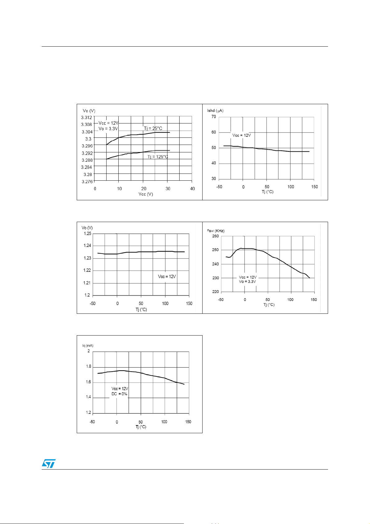
9 Typical characteristics
Figure 27. Line regulator Figure 28. Shutdown current vs junction
temperature
Figure 29. Output voltage vs junction
temperature
Figure 31. Quiescent current vs junction
temperature
Figure 30. Switching frequency vs
junction temperature
36/41
A5973D Typical characteristics
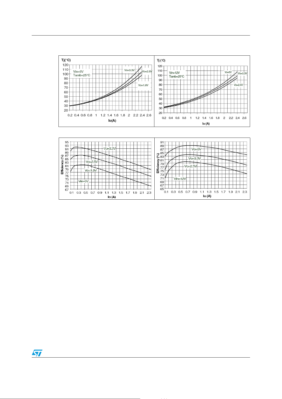
Figure 32. Junction temperature vs
Figure 34. Efficiency vs output current Figure 35. Efficiency vs output current
output current
Figure 33. Junction temperature vs
output current
37/41

A5973D Package mechanical data
10 Package mechanical data
In order to meet environmental requirements, ST offers these devices in different grades of
ECOPACK
specifications, grade definitions and product status are available at: www.st.com.
ECOPACK is an ST trademark.
®
packages, depending on their level of environmental compliance. ECOPACK®
38/41

A5973D Package mechanical data
Table 10. HSOP8 mechanical data
mm inch
Dim.
Min. Typ. Max. Min. Typ. Max.
A 1.70 0.0669
A1 0.00 0.10 0.00 0.0039
A2 1.25 0.0492
b 0.31 0.51 0.0122 0.0201
c 0.17 0.25 0.0067 0.0098
D 4.80 4.90 5.00 0.1890 0.1929 0.1969
D1 3 3.1 3.2 0.118 0.122 0.126
E 5.80 6.00 6.20 0.2283 0.2441
E1 3.80 3.90 4.00 0.1496 0.1575
E2 2.31 2.41 2.51 0.091 0.095 0.099
e1.27
h 0.25 0.50 0.0098 0.0197
L 0.40 1.27 0.0157 0.0500
k0° (min), 8° (max)
ccc 0.10 0.0039
Figure 36. Package dimensions
39/41
A5973D Revision history
11 Revision history
Table 11. Document revision history
Date Revision Changes
06-Aug-2007 1 Initial release
23-Oct-2007 2 Updated: Table 4 on page 6, Table 5 on page 10
07-Jan-2008 3 Updated Table 5 on page 10
06-May-2008 4 Updated Table 4 on page 6
29-Aug-2008 5 Updated Table 4 on page 6
07-Apr-2009 6 Updated Chapter 7 on page 16
40/41

A5973D
Please Read Carefully:
Information in this document is provided solely in connection with ST products. STMicroelectronics NV and its subsidiaries (“ST”) reserve the
right to make changes, corrections, modifications or improvements, to this document, and the products and services described herein at any
time, without notice.
All ST products are sold pursuant to ST’s terms and conditions of sale.
Purchasers are solely responsible for the choice, selection and use of the ST products and services described herein, and ST assumes no
liability whatsoever relating to the choice, selection or use of the ST products and services described herein.
No license, express or implied, by estoppel or otherwise, to any intellectual property rights is granted under this document. If any part of this
document refers to any third party products or services it shall not be deemed a license grant by ST for the use of such third party products
or services, or any intellectual property contained therein or considered as a warranty covering the use in any manner whatsoever of such
third party products or services or any intellectual property contained therein.
UNLESS OTHERWISE SET FORTH IN ST’S TERMS AND CONDITIONS OF SALE ST DISCLAIMS ANY EXPRESS OR IMPLIED
WARRANTY WITH RESPECT TO THE USE AND/OR SALE OF ST PRODUCTS INCLUDING WITHOUT LIMITATION IMPLIED
WARRANTIES OF MERCHANTABILITY, FITNESS FOR A PARTICULAR PURPOSE (AND THEIR EQUIVALENTS UNDER THE LAWS
OF ANY JURISDICTION), OR INFRINGEMENT OF ANY PATENT, COPYRIGHT OR OTHER INTELLECTUAL PROPERTY RIGHT.
UNLESS EXPRESSLY APPROVED IN WRITING BY AN AUTHORIZED ST REPRESENTATIVE, ST PRODUCTS ARE NOT
RECOMMENDED, AUTHORIZED OR WARRANTED FOR USE IN MILITARY, AIR CRAFT, SPACE, LIFE SAVING, OR LIFE SUSTAINING
APPLICATIONS, NOR IN PRODUCTS OR SYSTEMS WHERE FAILURE OR MALFUNCTION MAY RESULT IN PERSONAL INJURY,
DEATH, OR SEVERE PROPERTY OR ENVIRONMENTAL DAMAGE. ST PRODUCTS WHICH ARE NOT SPECIFIED AS "AUTOMOTIVE
GRADE" MAY ONLY BE USED IN AUTOMOTIVE APPLICATIONS AT USER’S OWN RISK.
Resale of ST products with provisions different from the statements and/or technical features set forth in this document shall immediately void
any warranty granted by ST for the ST product or service described herein and shall not create or extend in any manner whatsoever, any
liability of ST.
ST and the ST logo are trademarks or registered trademarks of ST in various countries.
Information in this document supersedes and replaces all information previously supplied.
The ST logo is a registered trademark of STMicroelectronics. All other names are the property of their respective owners.
© 2009 STMicroelectronics - All rights reserved
STMicroelectronics group of companies
Australia - Belgium - Brazil - Canada - China - Czech Republic - Finland - France - Germany - Hong Kong - India - Israel - Italy - Japan -
Malaysia - Malta - Morocco - Singapore - Spain - Sweden - Switzerland - United Kingdom - United States of America
www.st.com
41/41
 Loading...