

Up to 1 A step down switching regulator
Features
■ Qualified following the AEC-Q100
requirements (see PPAP for more details)
■ 1 A DC output current
■ Operating input voltage from 4 V to 36 V
■ 3.3 V / (±2%) reference voltage
■ Output voltage adjustable from 1.235 V to V
■
Low dropout operation: 100% duty cycle
■ 250 kHz Internally fixed frequency
■ Voltage feedforward
■ Zero load current operation
■ Internal current limiting
■ Inhibit for zero current consumption
■ Synchronization
■ Protection against feedback disconnection
■ Thermal shutdown
Application
■ Dedicated to automotive applications
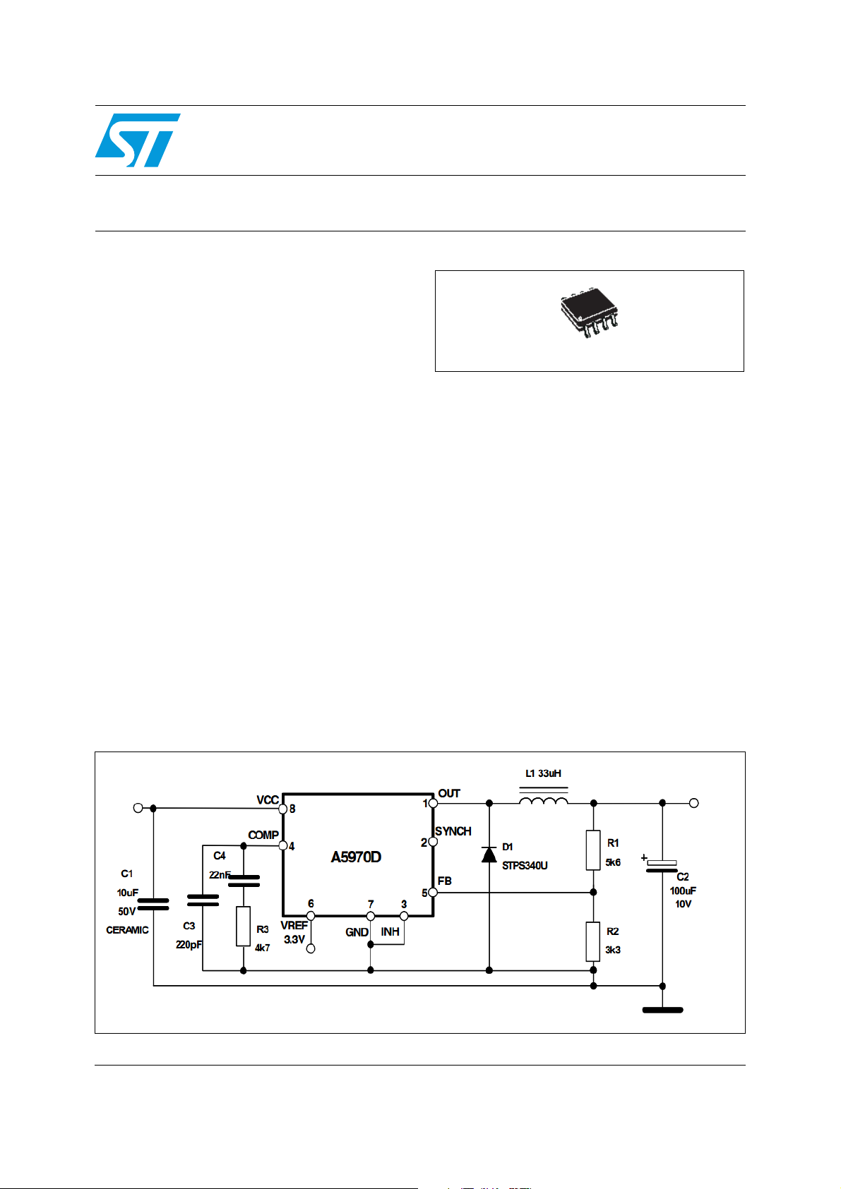
Figure 1. Application schematic
VIN=4 to 36V
A5970D
for automotive applications
SO8
IN
Description
The A5970D is a step down monolithic power
switching regulator with a minimum switch current
limit of 1.35 A so it is able to deliver up to 1 A DC
current to the load depending on the application
conditions. The output voltage can be set from
1.235 V to V
The device uses an internal p-channel DMOS
transistor (with a typical R
switching element to minimize the size of the
external components.
An internal oscillator fixes the switching frequency
at 250 kHz. Having a minimum input voltage of
4 V only it fits the automotive applications
requiring the device operation even in cold crank
conditions. Pulse by pulse current limit with the
internal frequency modulation offers an effective
constant current short circuit protection.
.
IN
of 250 mΩ) as
DS(on)
=3.3V
V
OUT
November 2009 Doc ID 13955 Rev 6 1/41
www.st.com
41

Contents A5970D
Contents
1 Pin settings . . . . . . . . . . . . . . . . . . . . . . . . . . . . . . . . . . . . . . . . . . . . . . . . 4
1.1 Pin connection . . . . . . . . . . . . . . . . . . . . . . . . . . . . . . . . . . . . . . . . . . . . . . 4
1.2 Pin description . . . . . . . . . . . . . . . . . . . . . . . . . . . . . . . . . . . . . . . . . . . . . . 4
2 Electrical data . . . . . . . . . . . . . . . . . . . . . . . . . . . . . . . . . . . . . . . . . . . . . . 5
2.1 Maximum ratings . . . . . . . . . . . . . . . . . . . . . . . . . . . . . . . . . . . . . . . . . . . . 5
2.2 Thermal data . . . . . . . . . . . . . . . . . . . . . . . . . . . . . . . . . . . . . . . . . . . . . . . 5
3 Electrical characteristics . . . . . . . . . . . . . . . . . . . . . . . . . . . . . . . . . . . . . 6
4 Datasheet parameters over the temperature range . . . . . . . . . . . . . . . . 8
5 Functional description . . . . . . . . . . . . . . . . . . . . . . . . . . . . . . . . . . . . . . . 9
5.1 Power supply and voltage reference . . . . . . . . . . . . . . . . . . . . . . . . . . . . . 9
5.2 Voltages monitor . . . . . . . . . . . . . . . . . . . . . . . . . . . . . . . . . . . . . . . . . . . . 10
5.3 Oscillator and synchronization . . . . . . . . . . . . . . . . . . . . . . . . . . . . . . . . . 10
5.4 Current protection . . . . . . . . . . . . . . . . . . . . . . . . . . . . . . . . . . . . . . . . . . . 11
5.5 Error amplifier . . . . . . . . . . . . . . . . . . . . . . . . . . . . . . . . . . . . . . . . . . . . . . 12
5.6 PWM comparator and power stage . . . . . . . . . . . . . . . . . . . . . . . . . . . . . 12
5.7 Inhibit function . . . . . . . . . . . . . . . . . . . . . . . . . . . . . . . . . . . . . . . . . . . . . 13
5.8 Thermal shutdown . . . . . . . . . . . . . . . . . . . . . . . . . . . . . . . . . . . . . . . . . . 14
6 Additional features and protection . . . . . . . . . . . . . . . . . . . . . . . . . . . . 15
6.1 Feedback disconnection . . . . . . . . . . . . . . . . . . . . . . . . . . . . . . . . . . . . . . 15
6.2 Output overvoltage protection . . . . . . . . . . . . . . . . . . . . . . . . . . . . . . . . . 15
6.3 Zero load . . . . . . . . . . . . . . . . . . . . . . . . . . . . . . . . . . . . . . . . . . . . . . . . . 15
7 Closing the loop . . . . . . . . . . . . . . . . . . . . . . . . . . . . . . . . . . . . . . . . . . . 16
7.1 Error amplifier and compensation network . . . . . . . . . . . . . . . . . . . . . . . . 17
7.2 LC filter . . . . . . . . . . . . . . . . . . . . . . . . . . . . . . . . . . . . . . . . . . . . . . . . . . . 18
7.3 PWM comparator . . . . . . . . . . . . . . . . . . . . . . . . . . . . . . . . . . . . . . . . . . . 19
8 Application information . . . . . . . . . . . . . . . . . . . . . . . . . . . . . . . . . . . . . 21
2/41 Doc ID 13955 Rev 6

A5970D Contents
8.1 Component selection . . . . . . . . . . . . . . . . . . . . . . . . . . . . . . . . . . . . . . . . 21
8.2 Layout considerations . . . . . . . . . . . . . . . . . . . . . . . . . . . . . . . . . . . . . . . . 24
8.3 Thermal considerations . . . . . . . . . . . . . . . . . . . . . . . . . . . . . . . . . . . . . . 24
8.4 Short-circuit protection . . . . . . . . . . . . . . . . . . . . . . . . . . . . . . . . . . . . . . . 26
8.5 Application circuit . . . . . . . . . . . . . . . . . . . . . . . . . . . . . . . . . . . . . . . . . . . 28
8.6 Positive buck-boost regulator . . . . . . . . . . . . . . . . . . . . . . . . . . . . . . . . . . 31
8.7 Negative buck-boost regulator . . . . . . . . . . . . . . . . . . . . . . . . . . . . . . . . . 32
8.8 Synchronization example . . . . . . . . . . . . . . . . . . . . . . . . . . . . . . . . . . . . . 33
8.9 Compensation network with MLCC at the output . . . . . . . . . . . . . . . . . . . 33
8.10 External SOFT_START network . . . . . . . . . . . . . . . . . . . . . . . . . . . . . . . . 35
9 Typical characteristics . . . . . . . . . . . . . . . . . . . . . . . . . . . . . . . . . . . . . . 36
10 Package mechanical data . . . . . . . . . . . . . . . . . . . . . . . . . . . . . . . . . . . . 38
11 Revision history . . . . . . . . . . . . . . . . . . . . . . . . . . . . . . . . . . . . . . . . . . . 40
Doc ID 13955 Rev 6 3/41
Pin settings A5970D
1 Pin settings
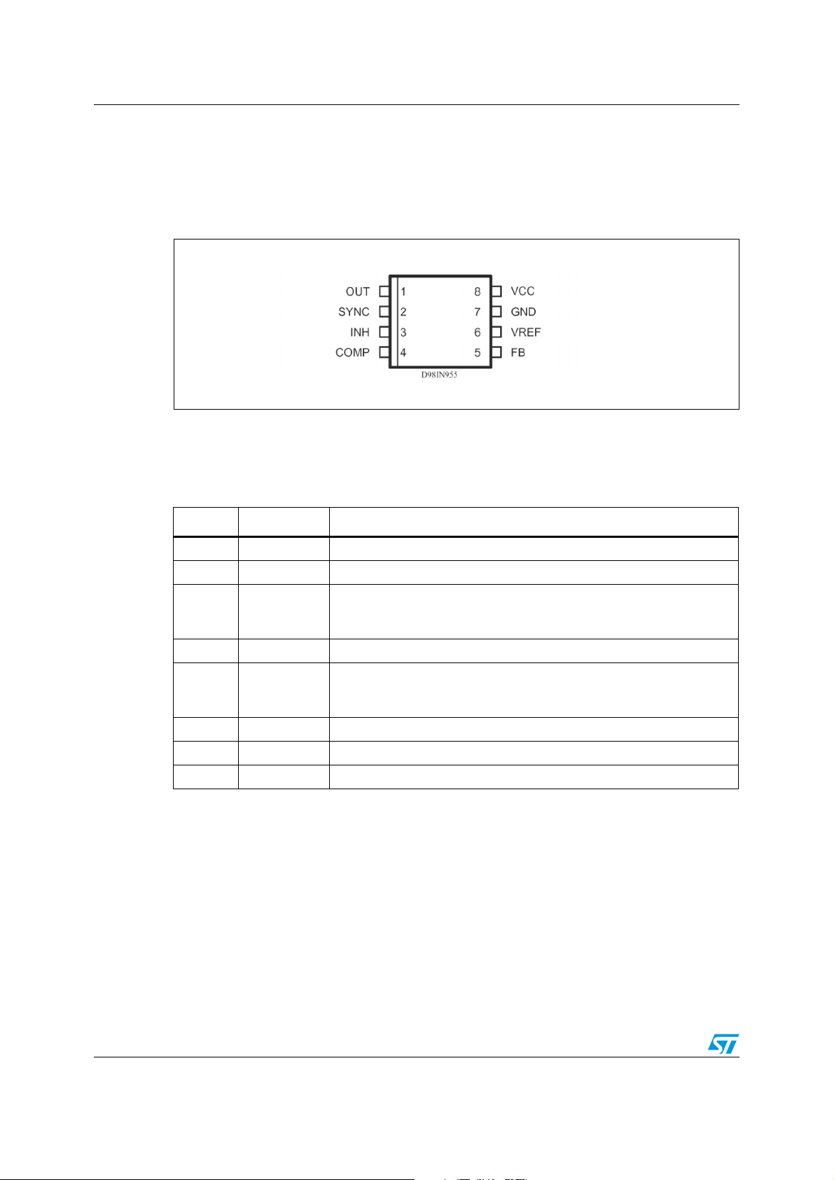
1.1 Pin connection
Figure 2. Pin connection (top view)
1.2 Pin description
Table 1. Pin description
N Pin Description
1 OUT Regulator output.
2 SYNCH Master/slave synchronization.
A logical signal (active high) disables the device. If INH not used the pin
3INH
4 COMP E/A output for frequency compensation.
5FB
6 VREF 3.3 V V
7 GND Ground.
8 VCC Unregulated DC input voltage.
must be grounded. When it is open an internal pull-up disable the
device.
Feedback input. Connecting directly to this pin results in an output
voltage of 1.23 V. An external resistive divider is required for higher
output voltages.
REF. No cap is requested for stability.
4/41 Doc ID 13955 Rev 6
A5970D Electrical data
2 Electrical data
2.1 Maximum ratings
Table 2. Absolute maximum ratings
Symbol Parameter Value Unit
V
8
V
1
I
1
V
, V
4
V
3
V
2
P
TOT
T
J
T
STG
Input voltage 40 V
OUT pin DC voltage
OUT pin peak voltage at Δt = 0.1 μs
Maximum output current int. limit.
Analog pins 4 V
5
INH -0.3 to V
SYNCH -0.3 to 4 V
Power dissipation at T
Operating junction temperature range -40 to 150 °C
Storage temperature range -55 to 150 °C
2.2 Thermal data
Table 3. Thermal data
Symbol Parameter Value Unit
R
thJA
1. Package mounted on evaluation board
Maximum thermal resistance junction-ambient 120
-1 to 40
-5 to 40
CC
≤ 70 °C 0.6 W
A
(1)
V
V
V
°C/W
Doc ID 13955 Rev 6 5/41
Electrical characteristics A5970D
3 Electrical characteristics
TJ = -40 °C to 125 °C, VCC = 12 V, unless otherwise specified.
Table 4. Electrical characteristics
Symbol Parameter Test condition Min. Typ. Max. Unit
V
R
DS(on)
f
CC
I
SW
Operating input
voltage range
MOSFET on
resistance
Maximum limiting
L
current
(1)
V
CC
= 5 V, TJ = 25 °C 1.5 1.87 2.25
V
CC
Switching frequency 212 250 280 kHz
Duty cycle 0 100 %
Dynamic characteristics (see test circuit).
V
η Efficiency V
Voltage feedback 4.4 V < V
5
= 5 V, V
0
DC characteristics
I
qop
I
qst-by
I
Total operating
quiescent current
Quiescent current Duty cycle=0; VFB=1.5 V 2.5 mA
q
> 2.2 V 50 100 μA
V
Total stand-by
quiescent current
inh
V
CC
V
inh
> 2.2 V
Inhibit
436V
0.250 0.5 Ω
= 5 V 1.35 1.87 2.25
< 36 V, 1.198 1.235 1.272 V
CC
= 12 V 90 %
CC
35mA
= 36 V;
80 150 μA
A
INH threshold voltage
Device ON 0.8 V
Device OFF 2.2 V
Error amplifier
V
OH
V
Io source
o sink Sink output current
I
I
High level output
voltage
Low level output
OL
voltage
Source output current
b Source bias current 2.5 4 μA
DC open loop gain R
gm Transconductance
= 1 V 3.5 V
V
FB
= 1.5 V 0.4 V
V
FB
V
= 1.9 V; VFB = 1 V
COMP
V
= 1.9 V; VFB=1.5 V
COMP
L=5065dB
I
= -0.1 mA to 0.1
COMP
mA; V
COMP
= 1.9 V
6/41 Doc ID 13955 Rev 6
190 300 μA
11.5 mA
2.3 mS

A5970D Electrical characteristics
Table 4. Electrical characteristics (continued)
Symbol Parameter Test condition Min. Typ. Max. Unit
Synch function
High input voltage V
Low input voltage V
Slave synch current
Master output
amplitude
Output pulse width no load, V
Reference section
Reference voltage
Line regulation
Load regulation I
Short circuit current 5 18 35 mA
1. With TJ = 85 °C, I
2. Guaranteed by design
lim_min
= 4.4 to 36 V; 2.5 V
CC
= 4.4 to 36 V; 0.74 V
CC
V
= 0.74 V
synch
V
= 2.33 V
synch
= 3 mA 2.75 3 V
I
source
I
= 0 to 5 mA
REF
VCC = 4.4 V to 36 V
I
= 0mA
REF
= 4.4 V to 36 V
V
CC
= 0 mA 8 15 mV
REF
= 1.5 A, assured by design, characterization and statistical correlation.
(2)
= 1.65 V 0.20 0.35 μs
synch
0.11
0.21
0.25
0.45
3.2 3.3 3.399 V
510mV
REF
V
mA
Doc ID 13955 Rev 6 7/41

Datasheet parameters over the temperature range A5970D
4 Datasheet parameters over the temperature range
The 100% of the population in the production flow is tested at three different ambient
temperatures (-40 °C; +25 °C, +125 °C) to guarantee the datasheet parameters inside the
junction temperature range (-40 °C; +125 °C).
The device operation is so guaranteed when the junction temperature is inside the (-40 °C;
+150 °C) temperature range. The designer can estimate the silicon temperature increase
respect to the ambient temperature evaluating the internal power losses generated during
the device operation (please refer to the Chapter 2.2).
However the embedded thermal protection disables the switching activity to protect the
device in case the junction temperature reaches the T
temperature.
All the datasheet parameters can be guaranteed to a maximum junction temperature of
+125 °C to avoid triggering the thermal shutdown protection during the testing phase
because of self heating.
SHTDWN
(+150 °C±10 °C)
8/41 Doc ID 13955 Rev 6
A5970D Functional description
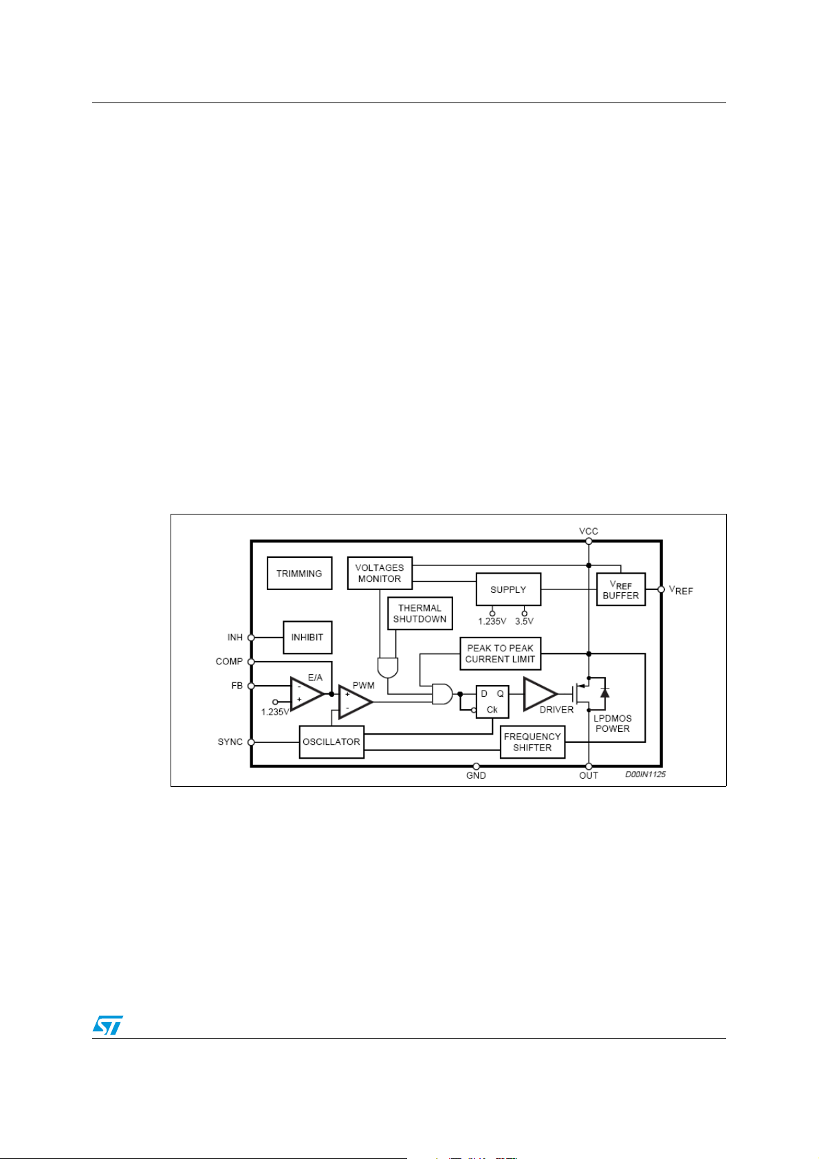
5 Functional description
The main internal blocks are shown in the device block diagram in Figure 3. They are:
● A voltage regulator supplying the internal circuitry. From this regulator, a 3.3 V
reference voltage is externally available.
● A voltage monitor circuit which checks the input and the internal voltages.
● A fully integrated sawtooth oscillator with a frequency of 250 kHz ± 15%, including also
the voltage feed forward function and an input/output synchronization pin.
● Two embedded current limitation circuits which control the current that flows through
the power switch. The pulse-by-pulse current limit forces the power switch OFF cycle
by cycle if the current reaches an internal threshold, while the frequency shifter reduces
the switching frequency in order to significantly reduce the duty cycle.
● A transconductance error amplifier.
● A pulse width modulator (PWM) comparator and the relative logic circuitry necessary to
drive the internal power.
● A high side driver for the internal P-MOS switch.
● An inhibit block for stand-by operation.
● A circuit to implement the thermal protection function.
Figure 3. Block diagram
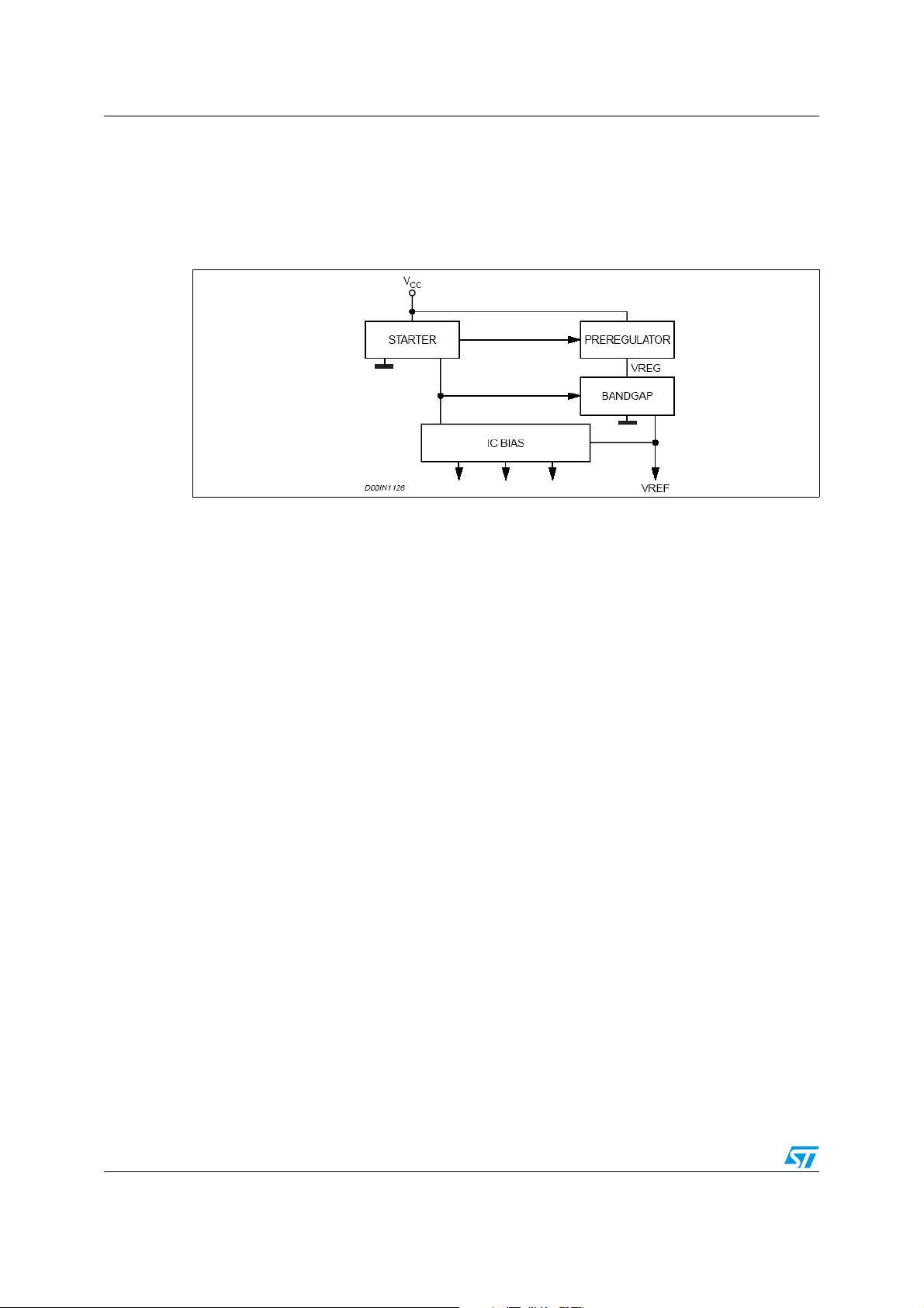
5.1 Power supply and voltage reference
The internal regulator circuit (shown in Figure 4) consists of a start-up circuit, an internal
voltage pre-regulator, the Bandgap voltage reference and the Bias block that provides
current to all the blocks. The Starter supplies the start-up currents to the entire device when
the input voltage goes high and the device is enabled (inhibit pin connected to ground). The
pre-regulator block supplies the Bandgap cell with a pre-regulated voltage V
very low supply voltage noise sensitivity.
that has a
REG
Doc ID 13955 Rev 6 9/41
Functional description A5970D
5.2 Voltages monitor
An internal block continuously senses the Vcc, V
their thresholds, the regulator begins operating. There is also a hysteresis on the V
(UVLO).
Figure 4. Internal circuit
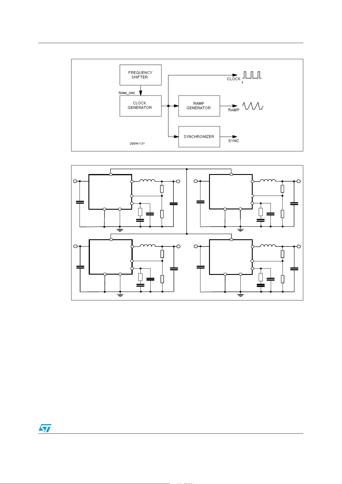
5.3 Oscillator and synchronization
Figure 5 shows the block diagram of the oscillator circuit.
The clock generator provides the switching frequency of the device, which is internally fixed
at 250 kHz. The frequency shifter block acts to reduce the switching frequency in case of
strong overcurrent or short circuit. The clock signal is then used in the internal logic circuitry
and is the input of the ramp generator and synchronizer blocks.
and Vbg. If the voltages go higher than
ref
CC
The ramp generator circuit provides the sawtooth signal, used for PWM control and the
internal voltage feed-forward, while the synchronizer circuit generates the synchronization
signal. The device also has a synchronization pin which can work both as master and slave.
Beating frequency noise is an issue when more than one voltage rail is on the same board.
A simple way to avoid this issue is to operate all the regulators at the same switching
frequency.
The synchronization feature of a set of the A5970D is simply get connecting together their
SYNCH pin. The device with highest switching frequency will be the MASTER and it
provides the synchronization signal to the others. Therefore the SYNCH is a I/O pin to
deliver or recognize a frequency signal. The synchronization circuitry is powered by the
internal reference (V
) so a small filtering capacitor (≥ 100 nF) connected between V
REF
REF
pin and the signal ground of the Master device is suggested for its proper operation.
However when a set of synchronized devices populates a board it is not possible to know in
advance the one working as Master, so the filtering capacitor have to be designed for whole
set of devices.
When one or more devices are synchronized to an external signal, its amplitude have to be
in comply with specifications given in the Tab l e 4 . The frequency of the synchronization
signal must be, at a minimum, higher than the maximum guaranteed natural switching
frequency of the device (275 kHz, see Tab le 4 ) while the duty cycle of the synchronization
signal can vary from approximately 10% to 90%. The small capacitor under V
REF
pin is
required for this operation.
10/41 Doc ID 13955 Rev 6
A5970D Functional description
Figure 5. Oscillator circuit block diagram
Figure 6. Synchronization example
OUT
OUT
SYNCH
SYNCH
SYNCH
A5970D
A5973D
A5973D
A5973D
OUT
OUT
OUT
FB
FB
FB
COMP
COMP
COMP
SYNCH
SYNCH
SYNCH
A5970D
A5973D
A5973D
A5973D
OUT
FB
FB
FB
COMP
COMP
COMP
SS/INH
SS/INH
SS/INH
SYNCH
SYNCH
SYNCH
A5970D
A5973D
A5973D
A5973D
SS/INH
SS/INH
SS/INH
GND
GND
GND
GND
GND
GND
OUT
OUT
OUT
FB
FB
FB
COMP
COMP
COMP
5.4 Current protection
The A5970D features two types of current limit protection: pulse-by-pulse and frequency
foldback.
The schematic of the current limitation circuitry for the pulse-by-pulse protection is shown in
Figure 7. The output power PDMOS transistor is split into two parallel PDMOS transistors.
The smallest one includes a resistor in series, R
R
switched off until the next falling edge of the internal clock pulse. Due to this reduction of the
ON time, the output voltage decreases. Since the minimum switch ON time necessary to
sense the current in order to avoid a false overcurrent signal is too short to obtain a
sufficiently low duty cycle at 250 kHz (see Chapter 8.4), the output current in strong
overcurrent or short circuit conditions could be not properly limited. For this reason the
switching frequency is also reduced, thus keeping the inductor current under its maximum
and if it reaches the threshold, the mirror becomes unbalanced and the PDMOS is
SENSE
SS/INH
SS/INH
SS/INH
SYNCH
SYNCH
SYNCH
A5970D
A5973D
A5973D
A5973D
SS/INH
SS/INH
SS/INH
. The current is sensed through
SENSE
GND
GND
GND
GND
GND
GND
OUT
OUT
OUT
FB
FB
FB
COMP
COMP
COMP
Doc ID 13955 Rev 6 11/41
Functional description A5970D
threshold. The frequency shifter (Figure 5) functions based on the feedback voltage. As the
feedback voltage decreases (due to the reduced duty cycle), the switching frequency
decreases also.
Figure 7. Current limitation circuitry
5.5 Error amplifier
The voltage error amplifier is the core of the loop regulation. It is a transconductance
operational amplifier whose non inverting input is connected to the internal voltage
reference (1.235 V), while the inverting input (FB) is connected to the external divider or
directly to the output voltage. The output (COMP) is connected to the external compensation
network. The uncompensated error amplifier has the following characteristics:
Table 5. Uncompensated error amplifier characteristics
Description Values
Transconductance 2300 µS
Low frequency gain 65 dB
Minimum sink/source voltage 1500 µA/300 µA
Output voltage swing 0.4 V/3.65 V
Input bias current 2.5 µA
The error amplifier output is compared to the oscillator sawtooth to perform PWM control.
5.6 PWM comparator and power stage
This block compares the oscillator sawtooth and the error amplifier output signals to
generate the PWM signal for the driving stage.
The power stage is a highly critical block, as it functions to guarantee a correct turn ON and
turn OFF of the PDMOS. The turn ON of the power element, or more accurately, the rise
time of the current at turn ON, is a very critical parameter. At a first approach, it appears that
the faster the rise time, the lower the turn ON losses.
However, there is a limit introduced by the recovery time of the recirculation diode.
12/41 Doc ID 13955 Rev 6
A5970D Functional description
In fact, when the current of the power element is equal to the inductor current, the diode
turns OFF and the drain of the power is able to go high. But during its recovery time, the
diode can be considered a high value capacitor and this produces a very high peak current,
responsible for numerous problems:
● Spikes on the device supply voltage that cause oscillations (and thus noise) due to the
board parasites.
● Turn ON overcurrent leads to a decrease in the efficiency and system reliability.
● Major EMI problems.
● Shorter freewheeling diode life.
The fall time of the current during turn OFF is also critical, as it produces voltage spikes (due
to the parasites elements of the board) that increase the voltage drop across the PDMOS.
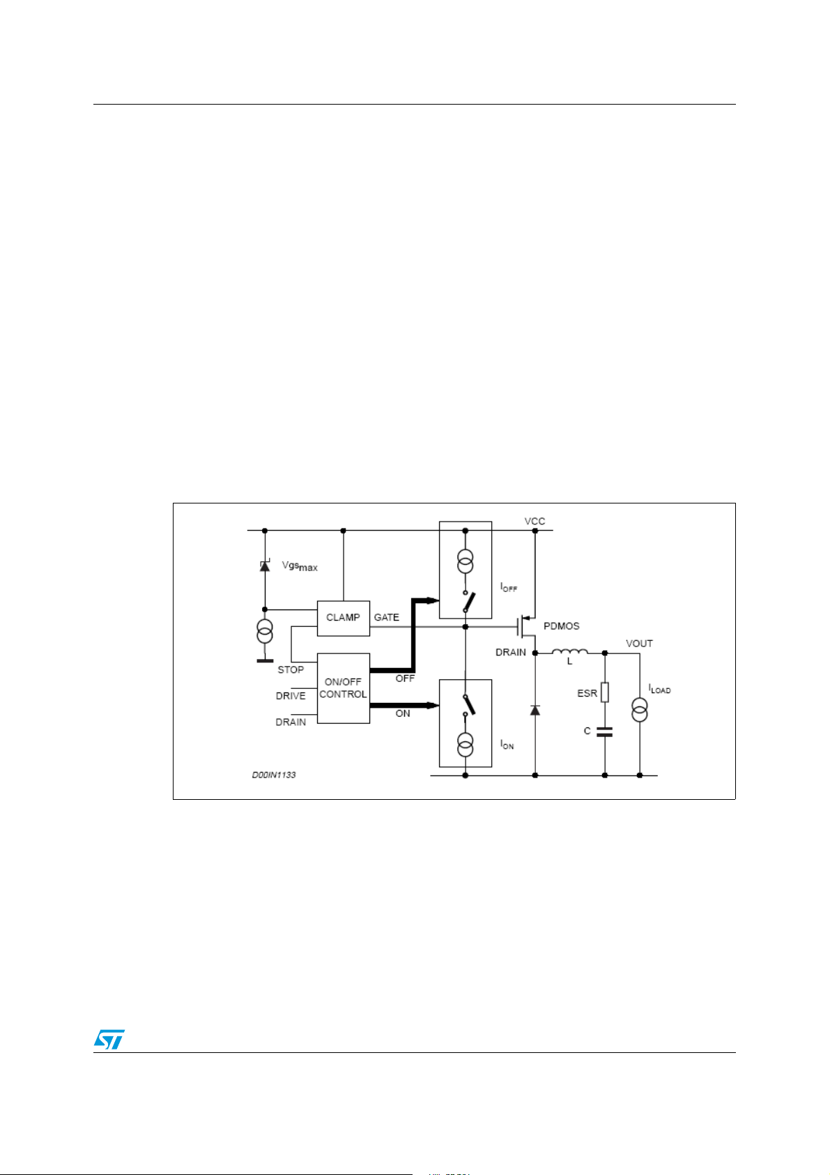
In order to minimize these problems, a new driving circuit topology has been used and the
block diagram is shown in Figure 8. The basic idea is to change the current levels used to
turn the power switch ON and OFF, based on the PDMOS and the gate clamp status.
This circuitry allows the power switch to be turned OFF and ON quickly and addresses the
freewheeling diode recovery time problem. The gate clamp is necessary to ensure that V
of the internal switch does not go higher than V
max. The ON/OFF Control block protects
GS
GS
against any cross conduction between the supply line and ground.
Figure 8. Driving circuitry
5.7 Inhibit function
The inhibit feature is used to put the device in standby mode. With the INH pin higher than
2.2 V the device is disabled and the power consumption is reduced to less than 100 µA.
With the INH pin lower than 0.8 V, the device is enabled. If the INH pin is left floating, an
internal pull up ensures that the voltage at the pin reaches the inhibit threshold and the
device is disabled. The pin is also V
compatible.
cc
Doc ID 13955 Rev 6 13/41
 Loading...