

查询74VHCT573AMTR供应商
WITH 3 STATE OUTPUT NON INVERTING
■ HIGHSPEED:t
■ LOW POWERDISSIPATION:
=4 µA (MAX.)at TA=25oC
I
CC
■ COMPATIBLEWITH TTL OUTPUTS:
=2V(MIN),VIL=0.8V(MAX)
V
IH
■ POWERDOWN PROTECTIONON INPUTS&
OUTPUTS
■ SYMMETRICALOUTPUT IMPEDANCE:
|I
|=IOL=8 mA (MIN)
OH
■ BALANCEDPROPAGATIONDELAYS:
t
≅ t
PLH
PHL
■ OPERATINGVOLTAGERANGE:
(OPR)= 4.5Vto 5.5V
V
CC
■ PINANDFUNCTIONCOMPATIBLEWITH
74SERIES573
■ IMPROVEDLATCH-UP IMMUNITY
■ LOWNOISE:V
DESCRIPTION
The 74VHCT573A is an advanced high-speed
CMOS OCTAL D-TYPE LATCH with 3 STATE
OUTPUT NON INVERTING fabricated with
sub-micron silicon gate and double-layer metal
wiringC
2
MOStechnology.
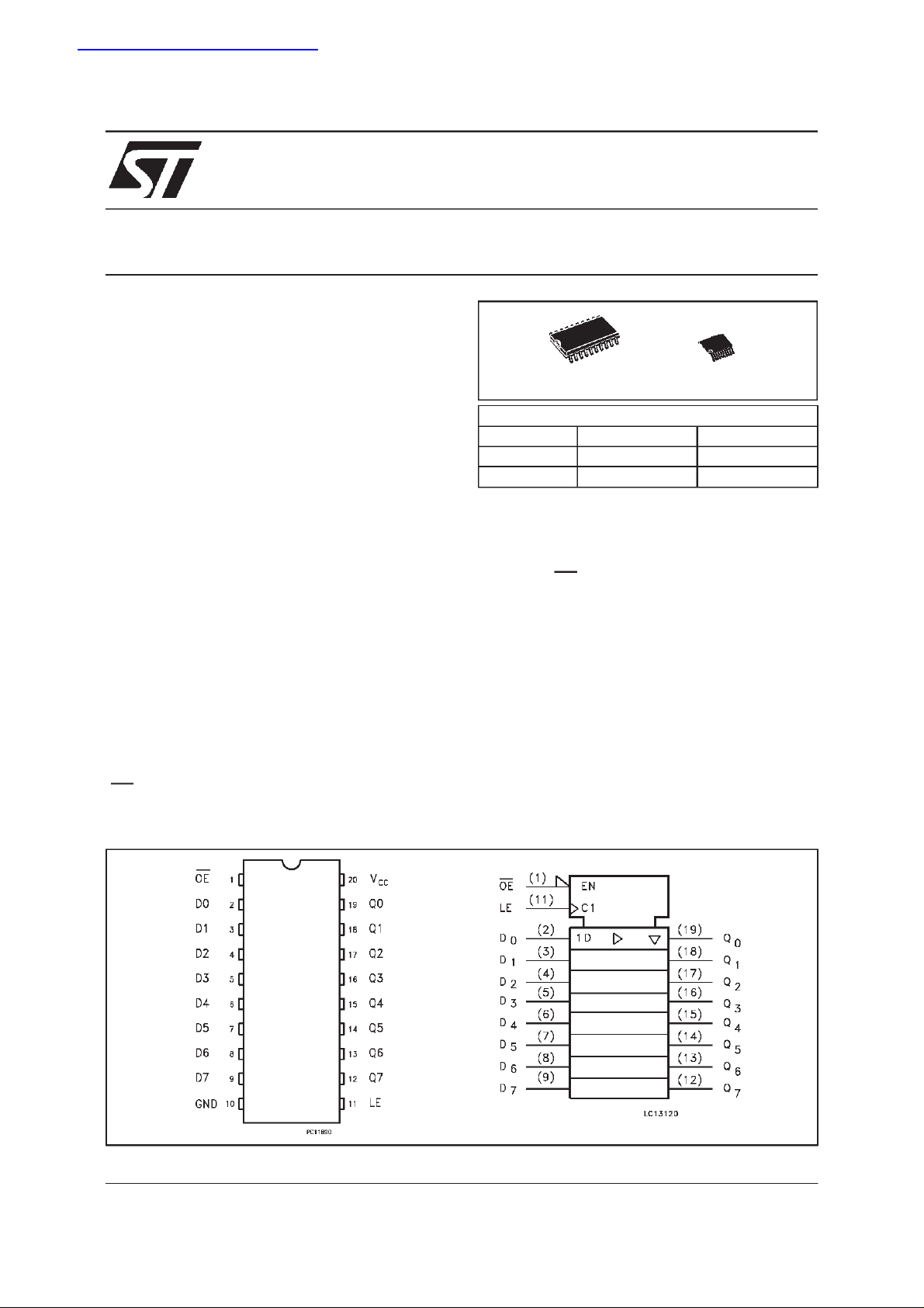
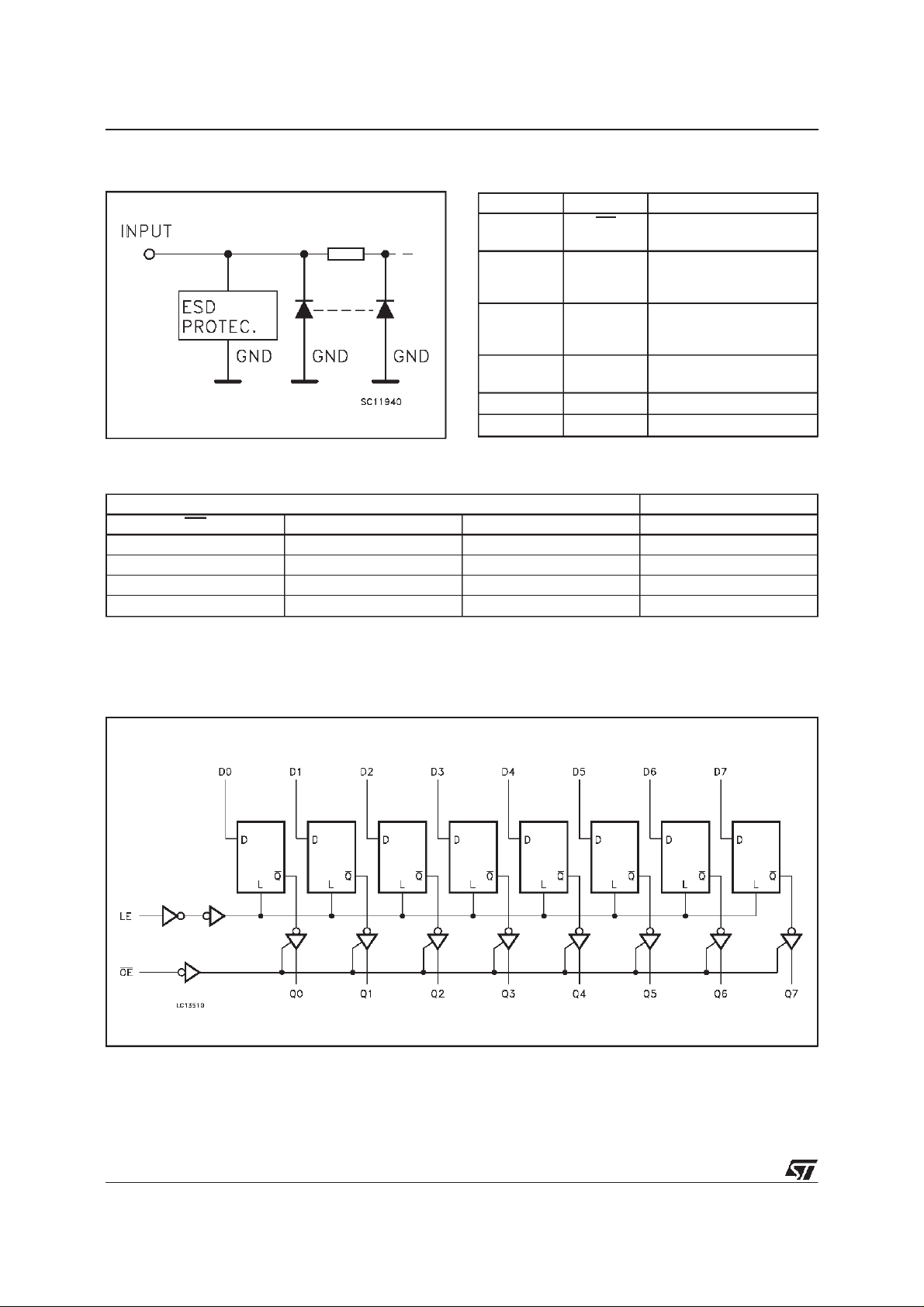
This 8 bit D-Type latch is controlled by a latch
enable input (LE) and an output enable input
(OE).
=5.4ns (TYP.)atVCC=5V
PD
= 0.9V(Max.)
OLP
74VHCT573A
OCTAL D-TYPE LATCH
SOP TSSOP
ORDER CODES
PACKAGE TUBE T & R
SOP 74VHCT573AM 74VHCT573AMTR
TSSOP 74VHCT573ATTR
While the LE input is held at a high level, the Q
outputswill follow the data inputs precisely.
When the LE is taken low, the Q outputs will be
latchedpreciselyat thelogic level of D input data.
While the (OE) input is low, the 8 outputs will be
in a normal logic state (high or low logic level)
and while high level the outputs will be in a high
impedancestate.
Power down protection is provided on all inputs
and outputs and 0 to 7V can be accepted on
inputs with no regard to the supply voltage. This
devicecan be used to interface 5V to 3V.
All inputs and outputs are equipped with
protection circuits against static discharge, giving
them 2KV ESD immunity and transient excess
voltage.
PIN CONNECTION AND IEC LOGIC SYMBOLS
February 2000
1/10
74VHCT573A
INPUT EQUIVALENTCIRCUIT PIN DESCRIPTION
PI N No SYMB OL NAME AND F U NCTI ON
1 OE 3 State Output Enable
2, 3, 4,
5, 6, 7,
8, 9
12, 13, 14,
15, 16, 17,
18, 19
11 LE Latch Enable
10 GND Ground (0V)
20 V
TRUTH TABLE
INPUTS OUTPUTS
OE LE D Q
HXXZ
L L X NO CHANGE *
LHLL
LHHH
X:Don’tcare
Z:Highimpedance
*Qoutputs arelatched atthetimewhentheLEinputistaken lowlogiclevel.
D0 to D7 Data Inputs
Q0 to Q7 3 State Latch Outputs
CC
Input (Active LOW)
Input
Positive Supply Voltage
LOGICDIAGRAM
2/10
74VHCT573A
ABSOLUTE MAXIMUM RATINGS
Symb o l Paramet er Value U n i t
V
V
V
V
I
I
OK
I
or I
I
CC
T
T
AbsoluteMaximumRatingsarethosevaluesbeyondwhichdamagetothedevicemayoccur. Functionaloperationunderthese conditionisnotimplied.
1)Outputin OFFState
2)HighorLowState
RECOMMENDEDOPERATINGCONDITIONS
Symb o l Paramet er Value Unit
V
V
V
V
T
dt/dv
1)Outputin OFFState
2)HighorLowState
from0.8Vto 2V
3)V
IN
Supply Voltage -0.5 to +7.0 V
CC
DC Input Voltage -0.5 to +7.0 V
I
DC Output Voltage (see note 1) -0.5 to +7.0 V
O
DC Output Voltage (see note 2) -0.5 to VCC+ 0.5 V
O
DC Input Diode Current - 20 mA
IK
DC Output Diode Current
DC Output Current
O
DC VCCor Ground Current ± 50 mA
GND
Storage Temperature -65 to +150
stg
Lead Temperature (10 sec) 300
L
Supply Voltage 4.5 to 5.5 V
CC
Input Voltage 0 to 5.5 V
I
Output Voltage (see note 1) 0 to 5.5 V
O
Output Voltage (see note 2) 0 to V
O
Operating Temperature -40 to +85
op
Input Rise and Fall Time (see note 3) (V
=5.0±0.5V)
CC
20 mA
±
25 mA
±
CC
0 to 20 ns/V
o
C
o
C
V
o
C
3/10
 Loading...