

74VHCT541A
OCTAL BUS BUFFER
WITH 3 STATE OUTPUTS (NON INVERTED)
■ HIGH SPEED: t
■ LOW POWER DISSIPATION:
I
= 4 µA (MAX.) at TA=25°C
CC
■ COMPATIBLE WITH TTL OUTP U TS:
V
= 2V (M IN.), V
IH
■ POWER DOWN PROTECTION ON INPUTS
= 4.1 ns (TYP.) at VCC = 5V
PD
= 0.8V (MAX)
IL
& OUTPUTS
■ SYMMETRICAL OUTPUT IMPEDANCE:
|I
| = IOL = 8 mA (MIN)
OH
■ BALANCED PROPAGATION DELAYS:
t
≅ t
PLH
PHL
■ OPERATING VOLTAGE RANGE:
V
(OPR) = 4.5V to 5.5V
CC
■ PIN AND FUNCTION COMPATIBLE WITH
74 SERIES 541
■ IMPROVED LATCH-UP IMMUNITY
■ LOW NOISE: V
= 0.9V (MAX.)
OLP
DESCRIPTION
The 74VHCT541A is an advanced high-speed
CMOS OCTAL BUS BUFFER (3-STATE)
fabricated with sub-micron silicon gate and
double-layer metal wiring C
2
MOS technology.
The 3 STATE control gate opera tes as two input
AND such that if either G1
and G2 are high, all
eight outputs are in the high impedance state.
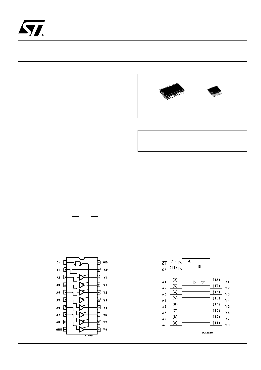
TSSOPSOP
Table 1: Order Codes
PACKAGE T & R
SOP 74VHCT541AMTR
TSSOP 74VHCT541ATTR
In order to enhance PC board layout, the
74VHCT541 offers a pinout having inputs and
outputs on opposite sides of the package.
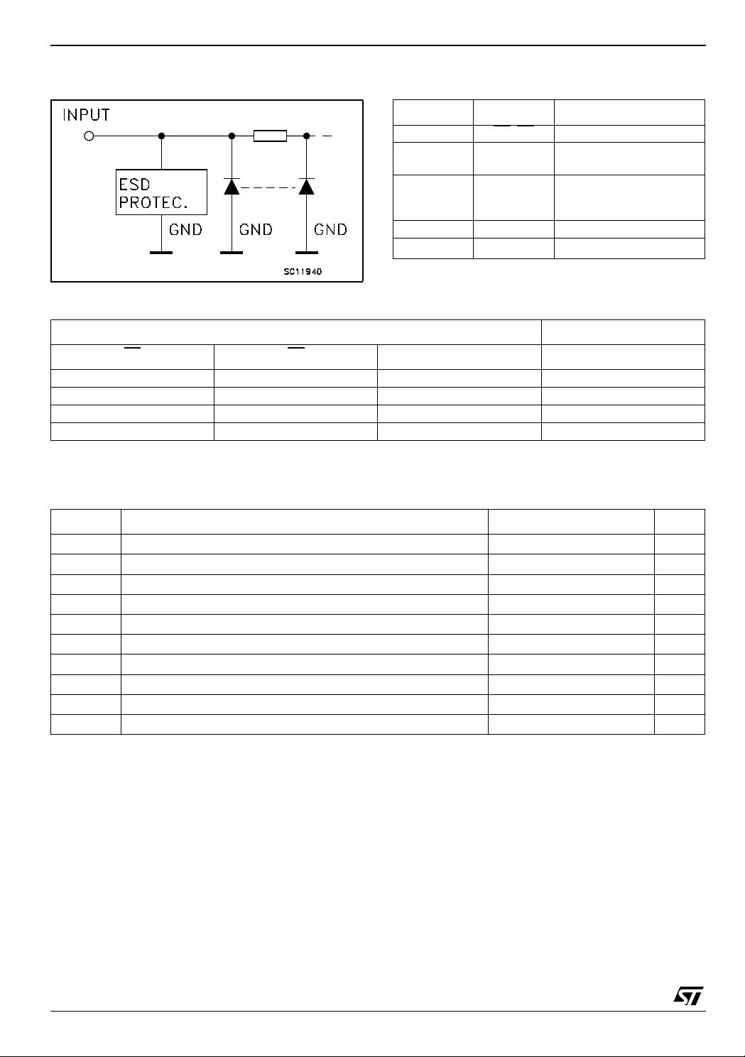
Power down protection is provided on all inputs
and outputs and 0 to 7V can be accepted on
inputs with no regard to the supply voltage. This
device can be used t o interf ace 5V to 3V s ince al l
inputs are equipped with TTL threshold.
All inputs and outputs are equipped with
protection circuits against static disc harge, giving
them 2KV ESD immunity and transient excess
voltage.
Figure 1: Pin Connection And IEC Logic Symbols
Rev. 4
1/12December 2004
74VHCT541A
Figure 2: Input Equivalent Circuit Table 2: Pin Description
PIN N° SYMBOL NAME AND FUNCTION
1, 19 G1
2, 3, 4, 5, 6,
7, 8, 9
18, 17, 16,
15, 14, 13,
12, 11
10 GND Ground (0V)
20 V
Table 3: Truth Table
INPUT OUTPUT
, G2 Output Enable Inputs
A1 to A8 Data Inputs
Y1 to Y8 Data Outputs
CC
Positive Supply Voltage
G1
G2 An Yn
HXXZ
XHXZ
LLHH
LLLL
X : Don’t Care
Z : High impedance
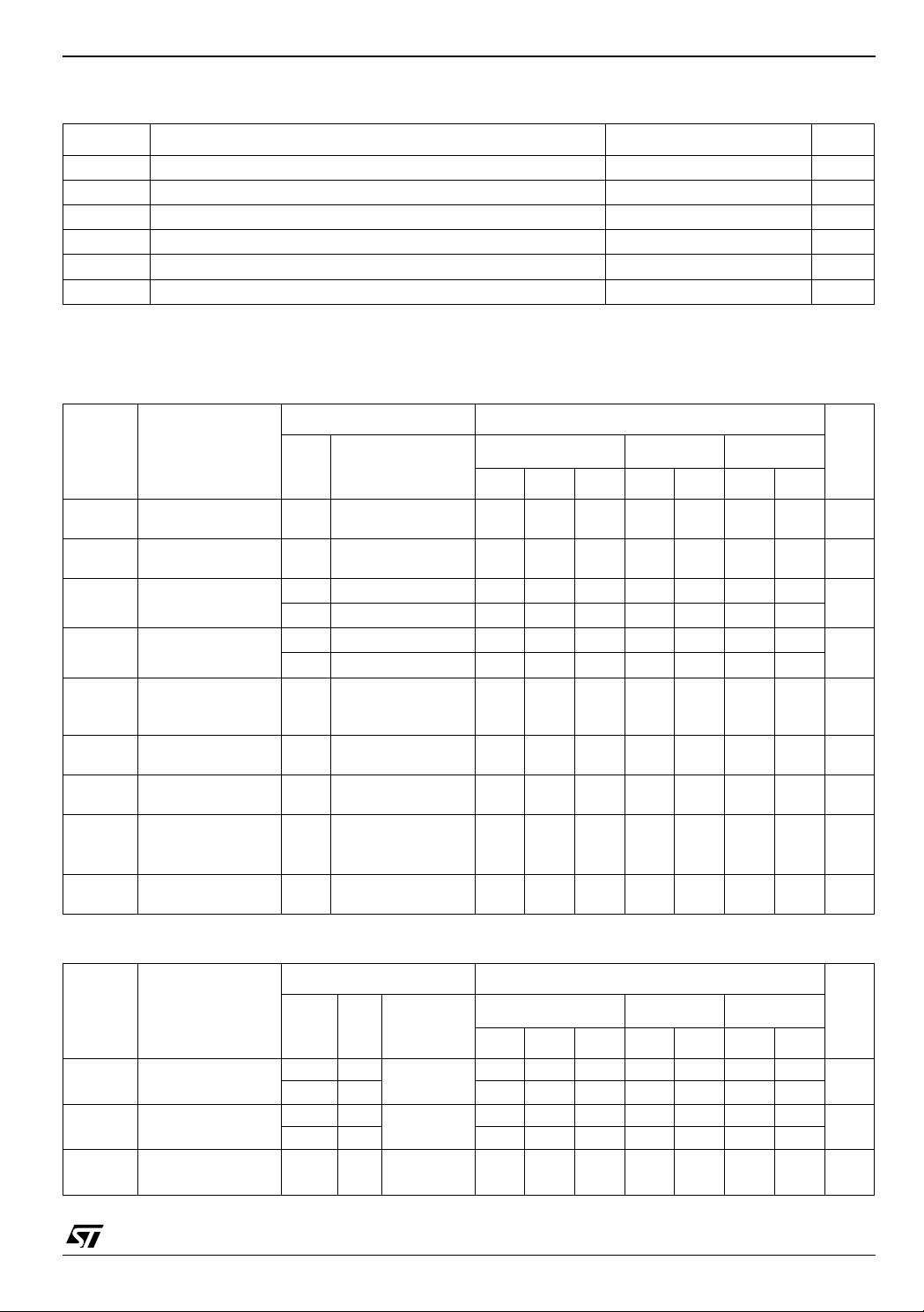
Table 4: Absolute Maximum Ratings
Symbol Parameter Value Unit
V
V
V
V
I
I
OK
I
I
or I
CC
T
T
Absolute Maximum Ratings are those values beyond which damage to the device may occur. Functional operation under these conditions is
not implied
1) Output in OFF State
2) High or Low State
Supply Voltage
CC
DC Input Voltage
I
DC Output Voltage (see note 1)
O
DC Output Voltage (see note 2) -0.5 to VCC + 0.5
O
DC Input Diode Current
IK
DC Output Diode Current
DC Output Current
O
DC VCC or Ground Current
GND
Storage Temperature
stg
Lead Temperature (10 sec)
L
-0.5 to +7.0 V
-0.5 to +7.0 V
-0.5 to +7.0 V
V
- 20 mA
± 20 mA
± 25 mA
± 50 mA
-65 to +150 °C
300 °C
2/12
74VHCT541A
Table 5: Recommended Operating Conditions
Symbol Parameter Value Unit
V
V
V
V
T
dt/dv
1) Output in OFF State
2) High or Low State
3) VIN from 0. 8V to 2V
Table 6: DC Specifications
Symbol Parameter
V
IH
V
IL
V
OH
V
OL
I
OZ
I
I
I
CC
+I
CC
I
OPD
Supply Voltage
CC
Input Voltage
I
Output Voltage (see note 1)
O
Output Voltage (see note 2) 0 to V
O
Operating Temperature
op
Input Rise and Fall Time (see note 3) (V
= 5.0 ± 0.5V)
CC
Test Condition Value
= 25°C
T
A
Min. Typ. Max. Min. Max. Min. Max.
222V
0.8 0.8 0.8 V
4.4 4.5 4.4 4.4
3.94 3.8 3.7
0.0 0.1 0.1 0.1
0.36 0.44 0.55
±0.25 ± 2.5 ± 2.5 µA
± 0.1 ± 1.0 ± 1.0 µA
44040µA
1.35 1.5 1.5 mA
0.5 5.0 5.0 µA
High Level Input
Voltage
Low Level Input
Voltage
High Level Output
Voltage
Low Level Output
Voltage
High Impedance
Output Leakage
Current
Input Leakage
Current
Quiescent Supply
Current
Additional Worst
Case Supply
Current
Output Leakage
Current
V
CC
(V)
4.5 to
5.5
4.5 to
5.5
4.5
4.5
4.5
4.5
4.5 to
5.5
0 to
5.5
5.5
5.5
0
=-50 µA
I
O
=-8 mA
I
O
IO=50 µA
I
=8 mA
O
= VIH or V
V
I
IL
VO = 0V to 5.5V
V
= 5.5V or GND
I
= VCC or GND
V
I
One Input at 3.4V,
other input at V
CC
or GND
= 5.5V
V
OUT
4.5 to 5.5 V
0 to 5.5 V
0 to 5.5 V
CC
-55 to 125 °C
0 to 20 ns/V
-40 to 85°C -55 to 125°C
V
Unit
V
V
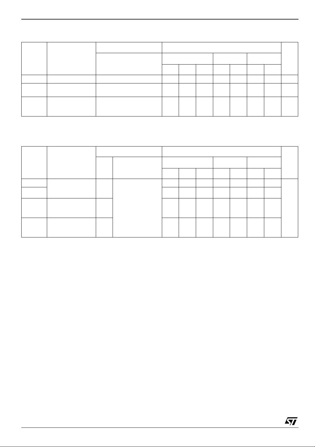
Table 7: AC Electrical Characteristics (Input t
Test Condition Value
Symbol Parameter
t
Propagation Delay
PLH
PHL
PZL
PZH
PLZ
PHZ
Time
Output Disable
Time
Output Enable
Time
t
t
t
t
t
(*) Voltage range is 5.0V ± 0.5V
V
(*)
(V)
C
(pF)
L
CC
5.0 15 4.1 6.0 1.0 6.5 1.0 6.5
5.0 50 6.2 8.5 1.0 9.5 1.0 9.5
5.0 15
5.0 50 7.5 10.0 1.0 12.0 1.0 12.0
RL = 1K
5.0 50 RL = 1K
= tf = 3ns)
r
= 25°C
T
A
-40 to 85°C -55 to 125°C
Min. Typ. Max. Min. Max. Min. Max.
Ω
Ω 7.0 10.0 1.0 12.0 1.0 12.0 ns
5.0 7.0 1.0 8.0 1.0 8.0
Unit
ns
ns
3/12
74VHCT541A
Table 8: Capacitive Characteristics
Test Condition Value
= 25°C
Symbol Parameter
T
A
Min. Typ. Max. Min. Max. Min. Max.
C
C
C
Input Capacitance
IN
Output
OUT
Capacitance
Power Dissipation
PD
Capacitance
610 10 10pF
8pF
16 pF
(note 1)
1) CPD is defined as the value of the IC’s internal equivalent capacitance which is calculated from the operating current consumption without
load. (Refer to Test Circuit). Average operating current can be obtained by the following equation. I
Table 9: Dynamic Switching Characteristics
Test Condition Value
= 25°C
Symbol Parameter
V
V
Dynamic Low
OLP
Voltage Quiet
OLV
Output (note 1, 2)
Dynamic High
V
IHD
Voltage Input
(note 1, 3)
Dynamic Low
V
ILD
Voltage Input
(note 1, 3)
V
CC
(V)
5.0
= 50 pF
5.0 2.0
C
L
5.0 0.8
T
A
Min. Typ. Max. Min. Max. Min. Max.
0.9 1.1
-1.1 -0.9
-40 to 85°C -55 to 125°C
= CPD x VCC x fIN + ICC/8 (per c ircuit )
CC(opr)
-40 to 85°C -55 to 125°C
Unit
Unit
V
1) Worst case package.
2) Max number of outp ut s defined as (n). Data inpu t s are driven 0V to 3.0V, (n-1) outputs switc hi ng and one output at GND.
3) Max number of data inputs (n) switching. (n-1) switching 0V to 3.0V. Inputs under test switching: 3.0V to threshold (V
(V
), f=1MHz.
IHD
ILD
), 0V to thresho l d
4/12

Figure 3: Test Circuit
t
, t
PLH
PHL
, t
t
PZL
PLZ
t
, t
PZH
PHZ
74VHCT541A
TEST SWITCH
Open
V
CC
GND
CL =15/50pF or equivalent (i ncludes jig an d probe capac i tance)
= R1 = 1KΩ or equivalent
R
L
R
= Z
of pulse generator (typically 50Ω)
T
OUT
Figure 4: Waveform - Propagation Delays (f=1MHz; 50% duty cycle)
5/12

74VHCT541A
Figure 5: Waveform - Output Enable And Disable Time (f=1MHz; 50% duty cycle)
6/12

SO-20 MECHANICAL DATA
74VHCT541A
DIM.
A 2.35 2.65 0.093 0.104
A1 0.1 0.30 0.004 0.012
B 0.33 0.51 0.013 0.020
C 0.23 0.32 0.009 0.013
D 12.60 13.00 0.496 0.512
E 7.4 7.6 0.291 0.299
e 1.27 0.050
H 10.00 10.65 0.394 0.419
h 0.25 0.75 0.010 0.030
L 0.4 1.27 0.016 0.050
k0° 8° 0° 8°
ddd 0.100 0.004
MIN. TYP MAX. MIN. TYP. MAX.
mm. inch
0016022D
7/12

74VHCT541A
TSSOP20 MECHANICAL DATA
mm. inch
DIM.
MIN. TYP MAX. MIN. TYP. MAX.
A 1.2 0.047
A1 0.05 0.15 0.002 0.004 0.006
A2 0.8 1 1.05 0.031 0.039 0.041
b 0.19 0.30 0.007 0.012
c 0.09 0.20 0.004 0.0079
D 6.4 6.5 6.6 0.252 0.256 0.260
E 6.2 6.4 6.6 0.244 0.252 0.260
E1 4.3 4.4 4.48 0.169 0.173 0.176
e 0.65 BSC 0.0256 BSC
K0˚ 8˚0˚ 8˚
L 0.45 0.60 0.75 0.018 0.024 0.030
A2
A
A1
b
e
K
c
L
E
D
E1
PIN 1 IDENTIFICATION
8/12
1
0087225C

74VHCT541A
Tape & Reel SO-20 MECHANICAL
mm. inch
DIM.
MIN. TYP MAX. MIN. TYP. MAX.
A 330 12.992
C 12.8 13.2 0.504 0.519
D 20.2 0.795
N 60 2.362
T 30.4 1.197
Ao 10.8 11 0.425 0.433
Bo 13.2 13.4 0.520 0.528
Ko 3.1 3.3 0.122 0.130
Po 3.9 4.1 0.153 0.161
P 11.9 12.1 0.468 0.476
DATA
9/12

74VHCT541A
Tape & Reel TSSOP20 MECHANICAL DATA
mm. inch
DIM.
MIN. TYP MAX. MIN. TYP. MAX.
A 330 12.992
C 12.8 13.2 0.504 0.519
D 20.2 0.795
N 60 2.362
T 22.4 0.882
Ao 6.8 7 0.268 0.276
Bo 6.9 7.1 0.272 0.280
Ko 1.7 1.9 0.067 0.075
Po 3.9 4.1 0.153 0.161
P 11.9 12.1 0.468 0.476
10/12

Table 10: Revision History
Date Revision Description of Change s
16-Dec-2004 4 Order Codes Revision - pag. 1.
74VHCT541A
11/12

74VHCT541A
Information fur nished is believed to be accurate and reliable. However, STMicroelectronics assumes no responsibility for the consequences
of use of s uch inf ormati on nor for a ny infr ing eme nt o f p atent s or o ther ri ghts of third parties wh ich m ay res ult fr om it s us e. No li cens e i s gr an ted
by implication or otherwise under any patent or patent rights of STMicroelectronics. Speci fications mentioned in this publication are subject
to change wi thout notice. This publication supersedes and replaces all information previously supplied. STMicroelectronics products are not
authorized for use as critical components in life support devices or systems without express written approval of STMicroelectronics.
The ST logo is a registered trademark of STMicroelectronics
All other names are the property of their respective owners
© 2004 STMicroelectronics - All Rights Reserved
STMicroelectronics group of companies
Australia - Belgium - Brazil - Canada - China - Czech Republic - Finland - France - Germany - Hong Kong - India - Israel - Italy - Japan -
Malaysia - Malta - Morocco - Singapore - Spain - Sweden - Switzerland - United Kingdom - United States of America
www.st.com
12/12
 Loading...