

ST 74VHCT32A User Manual
74VHCT32A
QUAD 2-INPUT OR GATE
■ HIGH SPEED: t
■ LOW POWER DISSIPATION:
I
= 2 µA (MAX.) at TA=25°C
CC
■ COMPA TIBLE WITH TTL OU TP U TS:
V
= 2V (MIN.), V
IH
■ POWER DOWN PROTECTION ON INPUTS
= 5 ns (TYP.) at VCC = 5V
PD
= 0.8V (MAX)
IL
& OUTPUTS
■ SYMMETRICAL OUTPUT IMPEDANCE:
|I
| = IOL = 8 mA (MIN)
OH
■ BALANCED PROPAGATION DELAYS:
t
≅ t
PLH
PHL
■ OPERATING VOLTAGE RANGE:
V
(OPR) = 4.5V to 5.5V
CC
■ PIN AND FUNCTION COMPATIBLE WITH
74 SERIES 32
■ IMPROVED LATCH-UP IMMUNITY
■ LOW NOISE: V
= 0.8V (MAX.)
OLP
DESCRIPTION
The 74VHCT32A is an advanced high-speed
CMOS QUAD 2-INPUT OR GATE fabricated with
sub-micron silicon gate and double-layer metal
wiring C
2
MOS technology.
The internal circuit is composed of 3 stages
including buffer ou tput, whi ch provid es hig h no ise
immunity and stable output.
TSSOPSOP
Table 1: Order Codes
PACKAGE T & R
SOP 74VHCT32AMTR
TSSOP 74VHCT32ATTR
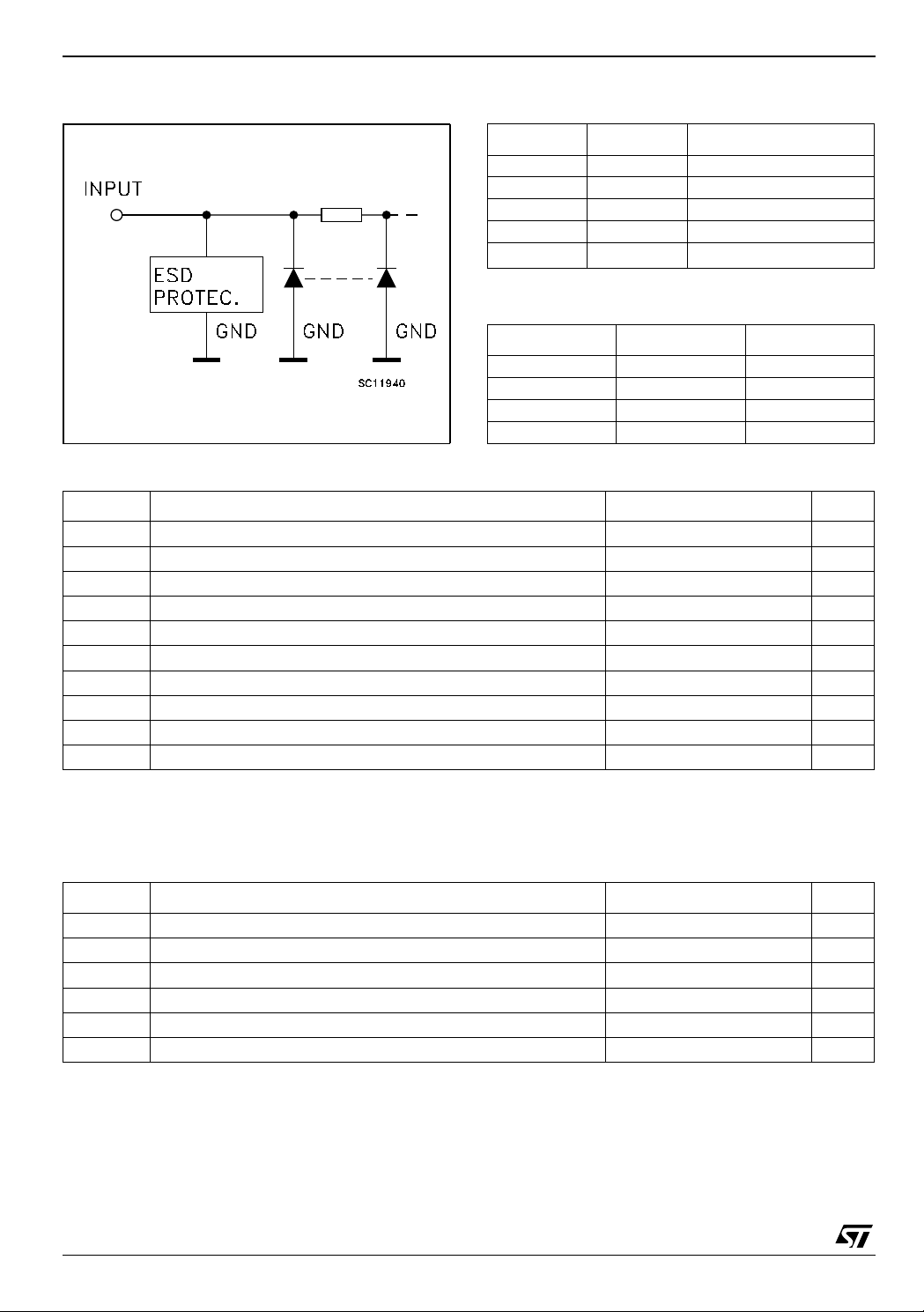
Power down protection is provided on all inputs
and outputs and 0 to 7V can be accepted on
inputs with no regard to the supply voltage. This
device can be used t o interf ace 5V to 3V s ince al l
inputs are equipped with TTL threshold.
All inputs and outputs are equipped with
protection circuits against static disc harge, giving
them 2KV ESD immunity and transient excess
voltage.
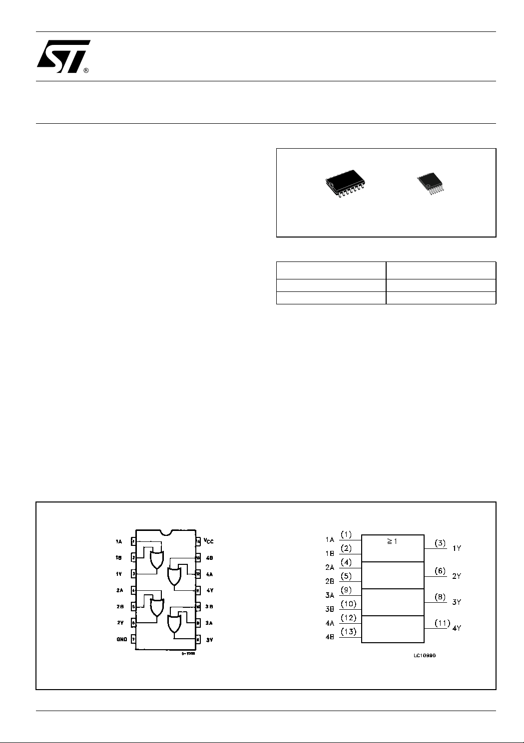
Figure 1: Pin Conne ction And IEC Logic Symbols
Rev. 4
1/11December 2004
74VHCT32A
Figure 2: Input Equivalent Circuit Table 2: Pin Description
PIN N° SYMBOL NAME AND FUNCTION
1, 4, 9, 12 1A to 4A Data Inputs
2, 5, 10, 13 1B to 4B Data Inputs
3, 6, 8, 11 1Y to 4Y Data Outputs
7 GND Ground (0V)
14
Table 3: Truth Table
ABY
LLL
LHH
HLH
HHH
Table 4: Absolute Maximum Ratings
Symbol Parameter Value Unit
V
V
V
V
I
I
OK
I
or I
I
CC
T
T
Absolute Maximum Ratings are those values beyond which damage to the device may occur. Functional operation under these conditions is
not implied
1) V
CC
2) High or Low State
Supply Voltage
CC
DC Input Voltage
I
DC Output Voltage (see note 1)
O
DC Output Voltage (see note 2) -0.5 to VCC + 0.5
O
DC Input Diode Current
IK
DC Output Diode Current
DC Output Current
O
DC VCC or Ground Current
GND
Storage Temperature
stg
Lead Temperature (10 sec)
L
= 0V
Table 5: Recommended Operating Conditions
V
CC
Positive Supply Voltage
-0.5 to +7.0 V
-0.5 to +7.0 V
-0.5 to +7.0 V
- 20 mA
± 20 mA
± 25 mA
± 50 mA
-65 to +150 °C
300 °C
V
Symbol Parameter Value Unit
V
V
V
V
T
dt/dv
1) V
CC
2) High or Low State
3) VIN from 0.8V to 2V
Supply Voltage
CC
Input Voltage
I
Output Voltage (see note 1)
O
Output Voltage (see note 2) 0 to V
O
Operating Temperature
op
Input Rise and Fall Time (see note 3) (V
= 0V
= 5.0 ± 0.5V)
CC
4.5 to 5.5 V
0 to 5.5 V
0 to 5.5 V
CC
-55 to 125 °C
0 to 20 ns/V
2/11
V
Table 6: DC Specifications
Symbol Parameter
V
V
V
+I
I
High Level Input
IH
Voltage
Low Level Input
V
IL
Voltage
High Level Output
OH
Voltage
Low Level Output
OL
Voltage
I
Input Leakage
I
Current
I
Quiescent Supply
CC
Current
Additional Worst
CC
Case Supply
Current
Output Leakage
OPD
Current
Test Condition Value
= 25°C
T
V
CC
(V)
4.5 to
5.5
A
Min. Typ. Max. Min. Max. Min. Max.
222V
4.5 to
5.5
4.5
4.5
4.5
4.5
0 to
VI = 5.5V or GND
5.5
V
5.5
I
O
=-8 mA
I
O
=50 µA
I
O
=8 mA
I
O
= VCC or GND
I
4.4 4.5 4.4 4.4
3.94 3.8 3.7
0.0 0.1 0.1 0.1
=-50 µA
One Input at 3.4V,
other input at V
5.5
CC
or GND
= 5.5V
0
V
OUT
74VHCT32A
-40 to 85°C -55 to 125°C
0.8 0.8 0.8 V
0.36 0.44 0.55
± 0.1 ± 1.0 ± 1.0 µA
22020µA
1.35 1.5 1.5 mA
0.5 5.0 5.0 µA
Unit
V
V
Table 7: AC Electrical Characteristics (Input t
= tf = 3ns)
r
Test Condition Value
= 25°C
Symbol Parameter
t
Propagation Delay
PLH
PHL
Time
t
(*) Voltage range is 5.0V ± 0.5V
V
(*)
(V)
C
(pF)
L
CC
5.0 15 5.0 7.0 1.0 8.0 1.0 8.0
5.0 50 5.5 8.0 1.0 9.0 1.0 9.0
T
A
-40 to 85°C -55 to 125°C
Min. Typ. Max. Min. Max. Min. Max.
Unit
ns
Table 8: Capacitive Characteristics
Test Condition Value
= 25°C
Symbol Parameter
T
A
Min. Typ. Max. Min. Max. Min. Max.
C
C
Input Capacitance
IN
Power Dissipation
PD
Capacitance
410 10 10pF
18 pF
(note 1)
1) CPD is defined as the value of the IC’s internal equivalent capacitance which is calculated from the operating current consumption without
load. (Refer to Test Circuit). Average operating current can be obtained by the following equation. I
-40 to 85°C -55 to 125°C
= CPD x VCC x fIN + ICC/4 (per gate)
CC(opr)
Unit
3/11
74VHCT32A
Table 9: Dynamic Switching Characteristics
Test Condition Value
= 25°C
Symbol Parameter
V
V
Dynamic Low
OLP
Voltage Quiet
OLV
Output (note 1, 2)
V
CC
(V)
5.0
T
A
Min. Typ. Max. Min. Max. Min. Max.
0.3 0.8
-0.8 -0.3
Dynamic High
V
IHD
Voltage Input
5.0 2.0
= 50 pF
C
L
(note 1, 3)
Dynamic Low
V
ILD
Voltage Input
5.0 0.8
(note 1, 3)
1) Worst case package.
2) Max number of outp ut s defined as (n). Data inpu t s are driven 0V to 3.0V, (n-1) outputs switc hi ng and one output at GND.
3) Max number of data inputs (n) switching. (n-1) switching 0V to 3.0V. Inputs under test switching: 3.0V to threshold (V
), f=1MHz.
(V
IHD
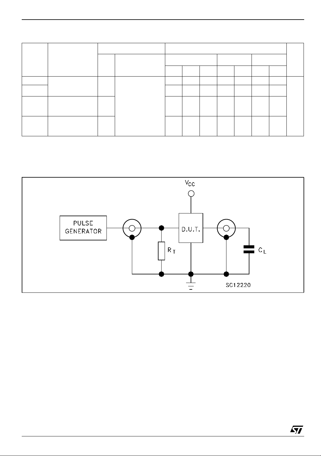
Figure 3: Test Cir cuit
-40 to 85°C -55 to 125°C
ILD
Unit
V
), 0V to thresho l d
CL =15/50pF or equivalent (i ncludes jig an d probe capac i tance)
R
= Z
of pulse generator (typically 50Ω)
T
OUT
4/11
 Loading...