

74VHCT273A
OCTAL D-TYPE FL IP FLO P W ITH CLEAR
■ HIGH SPEED:
f
= 170 MHz (TYP.) at VCC = 5V
MAX
■ LOW POWER DISSIPATION:
I
= 4 µA (MAX.) at TA=25°C
CC
■ COMPATIBLE WITH TTL OU TP U TS:
V
= 2V (MIN.), V
IH
■ POWER DOWN PROTECTION ON INPUTS
= 0.8V (MAX)
IL
& OUTPUTS
■ SYMMETRICAL OUTPUT IMPEDANCE:
|I
| = IOL = 8 mA (MIN)
OH
■ BALANCED PROPAGATION DELAYS :
t
≅ t
PLH
PHL
■ OPERATING VOLTAGE RANGE:
V
(OPR) = 4.5V to 5.5V
CC
■ PIN AND FUNCTION COMPATIBLE WITH
74 SERIES 273
■ IMPROVED LATCH-UP IMMUNIT Y
■ LOW NOISE: V
= 0.9V (MAX.)
OLP
DESCRIPTION
The 74VHCT273A is an advanced high-speed
CMOS OCTA L D-TY PE FL IP FL OP WIT H CLEA R
fabricated with sub-micron silicon gate and
double-layer metal wiring C
2
MOS technology.
Information signals applied to D inputs are
transferred to the Q o utputs on the positive going
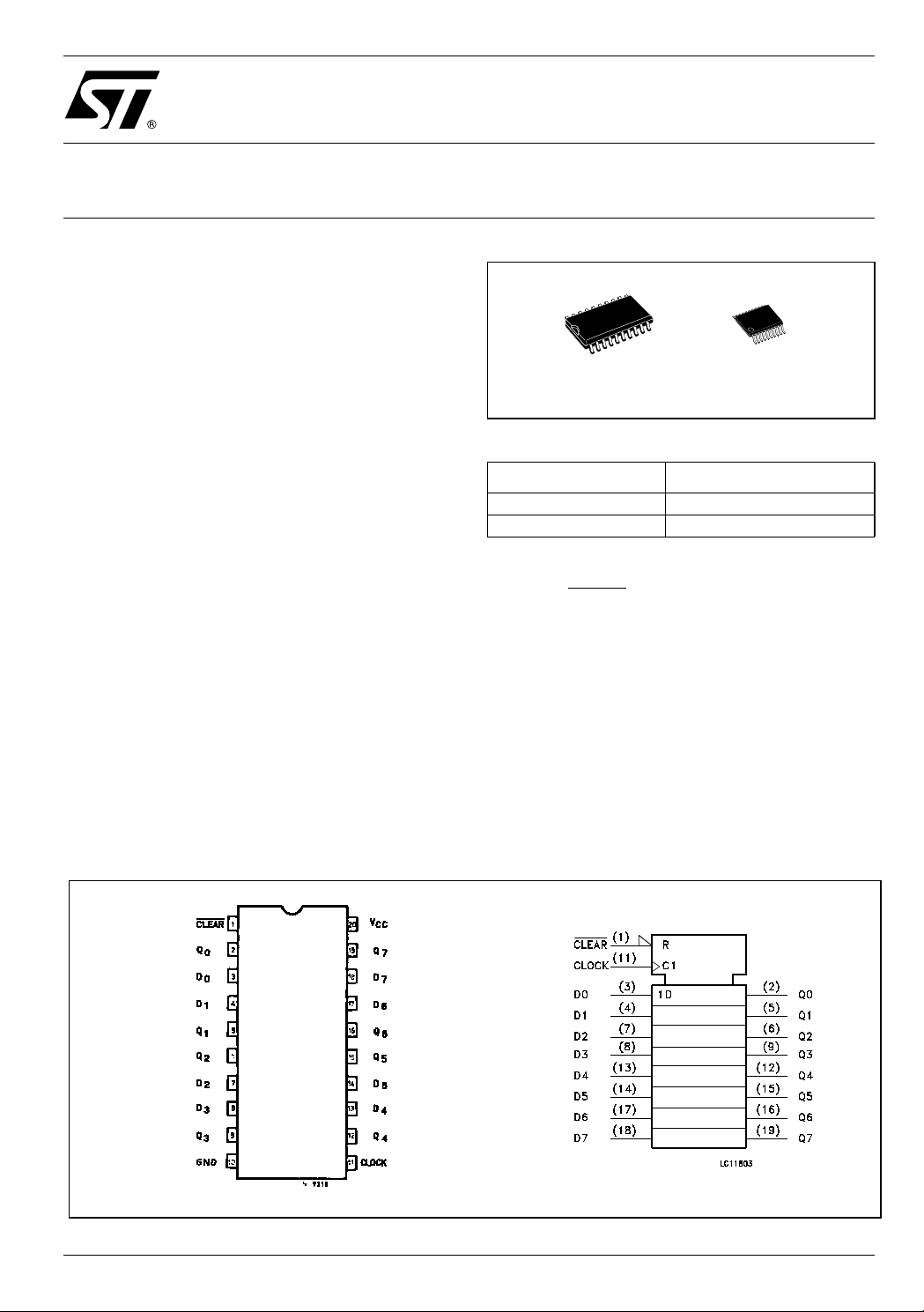
TSSOPSOP
Table 1: Order Codes
PACKAGE T & R
SOP 74VHCT273AMTR
TSSOP 74VHCT273ATTR
edge of the clock pulse.
When the CLE AR
input is held low, the Q outputs
are held low independently of the other inputs.
Power down protection is provided on all inputs
and outputs and 0 to 7V can be accepted on
inputs with no regard to the supply voltage. This
device can be used t o interf ace 5V to 3V s ince al l
inputs are equipped with TTL threshold.
All inputs and outputs are equipped with
protection circuits against static disc harge, giving
them 2KV ESD immunity and transient excess
voltage.
Figure 1: Pin Conne ction And IEC Logic Symbol s
Rev. 3
1/13December 2004
74VHCT273A
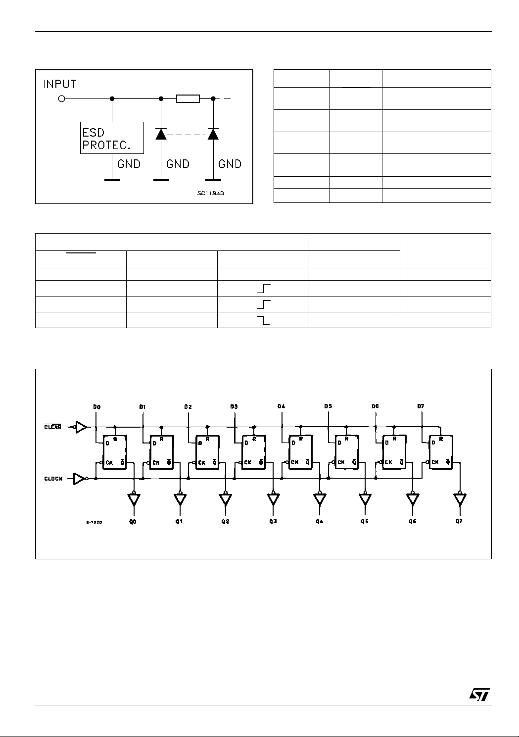
Figure 2: Input Equivalent Circuit Table 2: Pin Description
PIN N° SYMBOL NAME AND FUNCTION
Table 3: Truth Table
1CLEAR
2, 5, 6, 9, 12,
15, 16,19
3, 4, 7, 8, 13,
14, 17, 18
1 1 CLOCK Clock Input (LOW-to-HIGH
10 GND Ground (0V)
20 V
Q0 to Q7 Flip-Flop Outputs
D0 to D7 Data Inputs
CC
Asynchronous Master
Reset (Active LOW)
Edge Triggered)
Positive Supply Voltage
CLEAR
L X X L CLEAR
HL L
HH H
HX
X: Don’t care
Table 4: Logic Diagram
INPUTS OUTPUT
DCLOCKQ
Q
n
FUNCTION
NO CHANGE
This logi c di agram has not be used to est i m ate propaga tion delays
2/13
74VHCT273A
Table 5: Absolute Maximum Ratings
Symbol Parameter Value Unit
V
V
V
V
I
I
OK
I
or I
I
CC
T
T
Absolute Maximum Ratings are those values beyond which damage to the device may occur. Functional operation under these conditions is
not implied
1) V
CC
2) High or Low State
Table 6: Recommended Operating Conditions
Symbol Parameter Value Unit
V
V
V
V
T
dt/dv
Supply Voltage
CC
DC Input Voltage
I
DC Output Voltage (see note 1)
O
DC Output Voltage (see note 2) -0.5 to VCC + 0.5
O
DC Input Diode Current
IK
DC Output Diode Current
DC Output Current
O
DC VCC or Ground Current
GND
Storage Temperature
stg
Lead Temperature (10 sec)
L
= 0V
Supply Voltage
CC
Input Voltage
I
Output Voltage (see note 1)
O
Output Voltage (see note 2) 0 to V
O
Operating Temperature
op
Input Rise and Fall Time (see note 3) (V
= 5.0 ± 0.5V)
CC
-0.5 to +7.0 V
-0.5 to +7.0 V
-0.5 to +7.0 V
- 20 mA
± 20 mA
± 25 mA
± 50 mA
-65 to +150 °C
300 °C
4.5 to 5.5 V
0 to 5.5 V
0 to 5.5 V
CC
-55 to 125 °C
0 to 20 ns/V
V
V
1) V
= 0V
CC
2) High or Low State
3) V
from 0.8V to 2V
IN
3/13
74VHCT273A
Table 7: DC Specifications
Symbol Parameter
V
V
V
+I
I
High Level Input
IH
Voltage
Low Level Input
V
IL
Voltage
High Level Output
OH
Voltage
Low Level Output
OL
Voltage
I
Input Leakage
I
Current
I
Quiescent Supply
CC
Current
Additional Worst
CC
Case Supply
Current
Output Leakage
OPD
Current
Test Condition Value
= 25°C
T
V
CC
(V)
4.5 to
5.5
A
Min. Typ. Max. Min. Max. Min. Max.
222V
4.5 to
5.5
4.5
4.5
4.5
4.5
0 to
VI = 5.5V or GND
5.5
V
5.5
I
O
=-8 mA
I
O
=50 µA
I
O
=8 mA
I
O
= VCC or GND
I
4.4 4.5 4.4 4.4
3.94 3.8 3.7
0.0 0.1 0.1 0.1
=-50 µA
One Input at 3.4V,
other input at V
5.5
CC
or GND
= 5.5V
0
V
OUT
-40 to 85°C -55 to 125°C
Unit
0.8 0.8 0.8 V
V
0.36 0.44 0.55
V
± 0.1 ± 1.0 ± 1.0 µA
44040µA
1.35 1.5 1.5 mA
0.5 5.0 5.0 µA
Table 8: AC Electrical Characteristics (Input t
Test Condition Value
Symbol Parameter
t
Propagation Delay
PLH
t
t
Time CLOCK to Q
PHL
Propagation Delay
PHL
Time CLEAR
t
CLR Pulse Width
W
LOW
t
CK Pulse Width
W
HIGH or LOW
Setup Time D to
t
s
CLOCK, HIGH or
to Q
LOW
t
Hold Time D to CK,
h
HIGH or LOW
t
REM
f
t
OSLH
t
OSHL
Removal Time CLR
to CLOCK
Maximum Clock
MAX
Frequency
Output to Output
Skew time (note 1)
V
5.0
5.0
5.0
5.0
5.0
5.0
5.0
5.0
5.0
5.0
5.0
5.0
C
CC
(V)
L
(pF)
(**)
15 5.8 8.2 1.0 10.0 1.0 10.0
(**)
50 6.8 9.2 1.0 11.0 1.0 11.0
(**)
15 7.5 10.0 1.0 11.6 1.0 11.6
(**)
50 8.5 11.0 1.0 12.6 1.0 12.6
(**)
(**)
(**)
(**)
(**)
(**)
15 75 170 65 65
(**)
50 50 160 45 45
(**)
50 1.0 1.0 1.0 ns
= tf = 3ns)
r
= 25°C
T
A
-40 to 85°C -55 to 125°C
Min. Typ. Max. Min. Max. Min. Max.
5.0 5.0 5.0 ns
5.0 5.0 5.0 ns
2.0 2.0 2.0 ns
2.0 2.0 2.0 ns
1.0 1.0 1.0 ns
Unit
ns
ns
MHz
(*) Voltage range is 5.0V ± 0.5V
Note 1: Parameter guaranteed by design. t
4/13
soLH
= |t
pLHm
- t
pLHn
|, t
soHL
= |t
pHLm
- t
pHLn
|
 Loading...