

74VHCT244A
OCTAL BUS BUFFER
WITH 3 STATE OUTPUTS (NON INVERTED)
■ HIGH SPEED: t
■ LOW POWER DISSIPATION:
I
= 4 µA (MAX.) at TA=25°C
CC
■ COMPATIBLE WITH TTL OUTP U TS:
V
= 2V (M IN.), V
IH
■ POWER DOWN PROTECTION ON INPUTS
= 5.4 ns (TYP.) at VCC = 5V
PD
= 0.8V (MAX)
IL
& OUTPUTS
■ SYMMETRICAL OUTPUT IMPEDANCE:
| = IOL = 8 mA (MIN)
|I
OH
■ BALANCED PROPAGATION DELAYS:
≅ t
t
PLH
■ OPERATING VOLTAGE RANGE:
V
CC
■ PIN AND FUNCTION COMPATIBLE WITH
PHL
(OPR) = 4.5V to 5.5V
74 SERIES 244
■ IMPROVED LATCH-UP IMMUNITY
■ LOW NOISE: V
= 0.9V (MAX.)
OLP
DESCRIPTION
The 74VHCT244A is an advanced high-speed
CMOS OCTAL BUS BUFFER (3-STATE)
fabricated with sub-micron silicon gate and
double-layer metal wiring C
enable input governs four BUS BUFFERs.
G
2
MOS technology.
TSSOPSOP
Table 1: Order Codes
PACKAGE T & R
SOP 74VHCT244AMTR
TSSOP 74VHCT244ATTR
This device is designed to be used with 3 state
memory address drivers, etc.
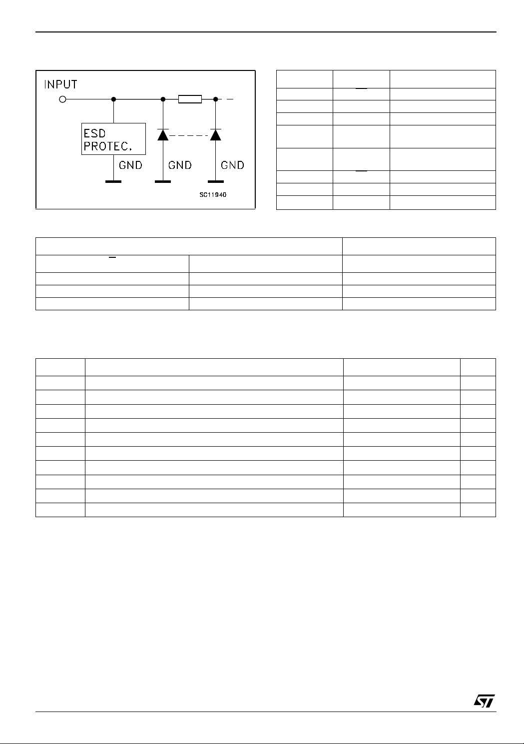
Power down protection is provided on all inputs
and outputs and 0 to 7V can be accepted on
inputs with no regard to the supply voltage. This
device can be used t o interf ace 5V to 3V s ince al l
inputs are equipped with TTL threshold.
All inputs and outputs are equipped with
protection circuits against static disc harge, giving
them 2KV ESD immunity and transient excess
voltage.
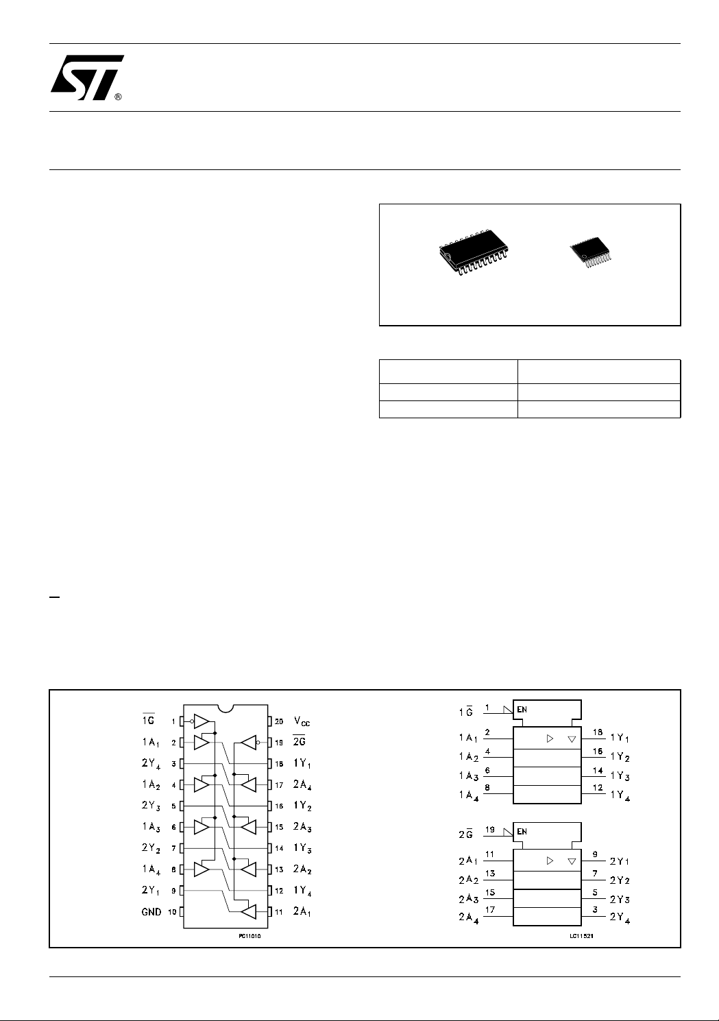
Figure 1: Pin Connection And IEC Logic Symbols
Rev. 4
1/12December 2004
74VHCT244A
Figure 2: Input Equivalent Circuit Table 2: Pin Description
PIN N° SYMBOL NAME AND FUNCTION
11G
2, 4, 6, 8 1A1 to 1A4 Data Inputs
9, 7, 5, 3 2Y1 to 2Y4 Data Outputs
11, 13, 15, 172A1 to 2A4 Data Inputs
18, 16, 14, 121Y1 to 1Y4 Data Outputs
Output Enable Input
19 2G
Output Enable Input
10 GND Ground (0V)
20 V
CC
Positive Supply Voltage
Table 3: Truth Table
INPUTS OUTPUT
G
An Yn
LLL
LHH
HXZ
X : Don’t Care
Z : High Impedance
Table 4: Absolute Maximum Ratings
Symbol Parameter Value Unit
V
V
V
V
I
I
OK
I
I
or I
CC
T
T
Absolute Maximum Ratings are those values beyond which damage to the device may occur. Functional operation under these conditions is
not implied
1) Output in OFF State
2) High or Low State
Supply Voltage
CC
DC Input Voltage
I
DC Output Voltage (see note 1)
O
DC Output Voltage (see note 2) -0.5 to VCC + 0.5
O
DC Input Diode Current
IK
DC Output Diode Current
DC Output Current
O
DC VCC or Ground Current
GND
Storage Temperature
stg
Lead Temperature (10 sec)
L
-0.5 to +7.0 V
-0.5 to +7.0 V
-0.5 to +7.0 V
V
- 20 mA
± 20 mA
± 25 mA
± 50 mA
-65 to +150 °C
300 °C
2/12
74VHCT244A
Table 5: Recommended Operating Conditions
Symbol Parameter Value Unit
V
V
V
V
T
dt/dv
1)Output in OFF State
2) High or Low State
3) VIN from 0. 8V to 2V
Table 6: DC Specifications
Symbol Parameter
V
IH
V
IL
V
OH
V
OL
I
OZ
I
I
I
CC
+I
CC
I
OPD
Supply Voltage
CC
Input Voltage
I
Output Voltage (see note 1)
O
Output Voltage (see note 2) 0 to V
O
Operating Temperature
op
Input Rise and Fall Time (see note 3) (V
= 5.0 ± 0.5V)
CC
Test Condition Value
= 25°C
T
A
Min. Typ. Max. Min. Max. Min. Max.
222V
0.8 0.8 0.8 V
4.4 4.5 4.4 4.4
3.94 3.8 3.7
0.0 0.1 0.1 0.1
0.36 0.44 0.55
±0.25 ± 2.5 ± 2.5 µA
± 0.1 ± 1.0 ± 1.0 µA
22020µA
1.35 1.5 1.5 mA
0.5 5.0 5.0 µA
High Level Input
Voltage
Low Level Input
Voltage
High Level Output
Voltage
Low Level Output
Voltage
High Impedance
Output Leakage
Current
Input Leakage
Current
Quiescent Supply
Current
Additional Worst
Case Supply
Current
Output Leakage
Current
V
CC
(V)
4.5 to
5.5
4.5 to
5.5
4.5
4.5
4.5
4.5
4.5 to
5.5
0 to
5.5
5.5
5.5
0
=-50 µA
I
O
=-8 mA
I
O
IO=50 µA
I
=8 mA
O
= VIH or V
V
I
IL
VO = 0V to 5.5V
V
= 5.5V or GND
I
= VCC or GND
V
I
One Input at 3.4V,
other input at V
CC
or GND
= 5.5V
V
OUT
4.5 to 5.5 V
0 to 5.5 V
0 to 5.5 V
CC
-55 to 125 °C
0 to 20 ns/V
-40 to 85°C -55 to 125°C
V
Unit
V
V
Table 7: AC Electrical Characteristics (Input t
Test Condition Value
Symbol Parameter
t
Propagation Delay
PLH
PHL
PLZ
PHZ
PZL
PZH
Time
Output Disable
Time
Output Enable
Time
t
t
t
t
t
(*) Voltage range is 5.0V ± 0.5V
V
(*)
(V)
C
(pF)
L
CC
5.0 15 5.4 7.4 1.0 8.5 1.0 8.5
5.0 50 5.9 8.4 1.0 9.5 1.0 9.5
5.0 15
5.0 50 8.2 11.4 1.0 13.0 1.0 13.0
RL = 1KΩ
5.0 50 RL = 1K Ω 8.8 11.4 1.0 13.0 1.0 13.0 ns
= tf = 3ns)
r
= 25°C
T
A
-40 to 85°C -55 to 125°C
Min. Typ. Max. Min. Max. Min. Max.
7.7 10.4 1.0 12.0 1.0 12.0
Unit
ns
ns
3/12
74VHCT244A
Table 8: Capacitive Characteristics
Test Condition Value
= 25°C
Symbol Parameter
T
A
Min. Typ. Max. Min. Max. Min. Max.
C
C
C
Input Capacitance
IN
Output
OUT
Capacitance
Power Dissipation
PD
Capacitance
610 10 10pF
10 pF
18 pF
(note 1)
1) CPD is defined as the value of the IC’s internal equivalent capacitance which is calculated from the operating current consumption without
load. (Refer to Test Circuit). Average operating current can be obtained by the following equation. I
Table 9: Dynamic Switching Characteristics
Test Condition Value
= 25°C
Symbol Parameter
V
V
Dynamic Low
OLP
Voltage Quiet
OLV
Output (note 1, 2)
Dynamic High
V
IHD
Voltage Input
(note 1, 3)
Dynamic Low
V
ILD
Voltage Input
(note 1, 3)
V
CC
(V)
5.0
= 50 pF
5.0 2.0
C
L
5.0 0.8
T
A
Min. Typ. Max. Min. Max. Min. Max.
0.9 1.1
-1.1 -0.9
-40 to 85°C -55 to 125°C
= CPD x VCC x fIN + ICC/8 (per gate)
CC(opr)
-40 to 85°C -55 to 125°C
Unit
Unit
V
1) Worst case package.
2) Max number of outp ut s defined as (n). Data inpu t s are driven 0V to 3.0V, (n-1) outputs switc hi ng and one output at GND.
3) Max number of data inputs (n) switching. (n-1) switching 0V to 3.0V. Inputs under test switching: 3.0V to threshold (V
(V
), f=1MHz.
IHD
ILD
), 0V to thresho l d
4/12
 Loading...