

ST 74VHC74 User Manual
74VHC74
DUAL D-TYPE FLIP FLOP WITH PRESET AND CLEAR
■ HIGH SPEED:
f
= 170 MHz (TYP.) at VCC = 5V
MAX
■ LOW POWER DISSIPATION :
I
= 2 µA (MAX.) at TA=25°C
CC
■ HIGH NOISE IMMUNITY:
V
= V
NIH
■ POWER DOWN PROTECTION ON INPUTS
■ SYMMETRICAL OUTPUT IMPEDANCE:
|I
| = IOL = 8 mA (MIN)
OH
■ BALANCED PROPAGATION DELAYS :
t
≅ t
PLH
■ OPERATING VOLTAGE RANGE:
V
(OPR) = 2V to 5.5V
CC
■ PIN AND FUNCTION COMPATIBLE WITH
= 28% VCC (MIN.)
NIL
PHL
74 SERIES 74
■ IMPROVED LATCH-UP IMMUNIT Y
DESCRIPTION
The 74VHC74 is an advanced high-speed CMOS
DUAL D-TYPE FLIP FLOP WITH PRESET AND
CLEAR fabricated with sub-micron silicon gate
and double-layer metal wiring C
2
MOS technology.
A signal on the D INPUT is transferred to the Q
OUTPUTS during the positive go ing transition of
the clock pulse.
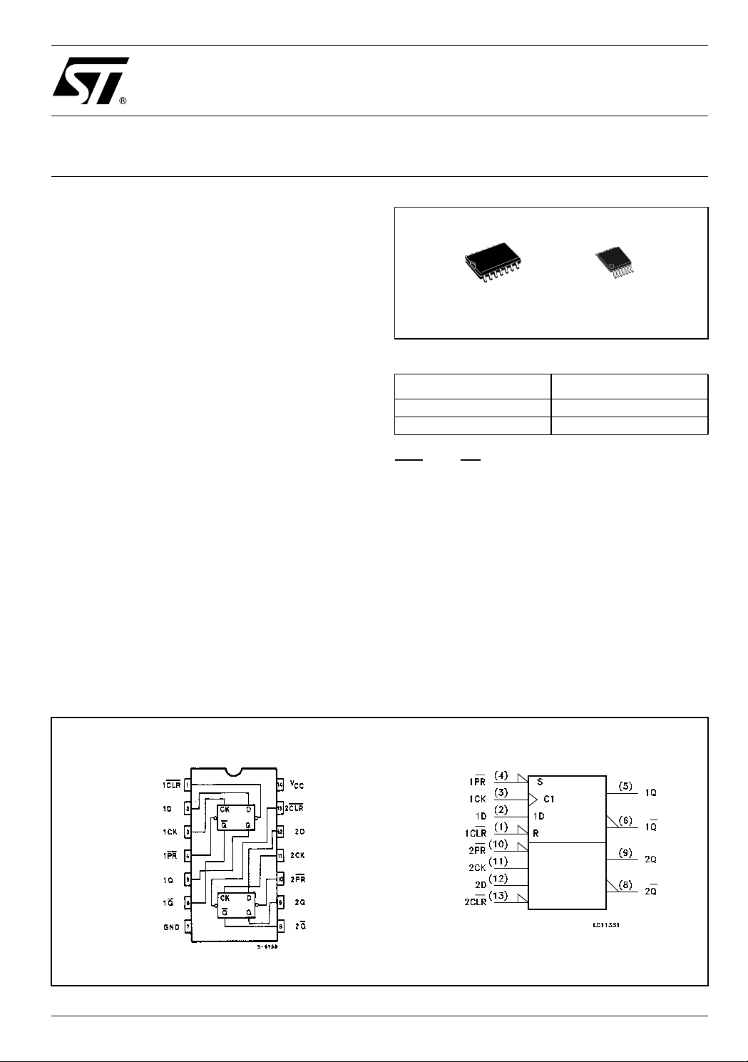
TSSOPSOP
Table 1: Order Codes
PACKAGE T & R
SOP 74VHC74MTR
TSSOP 74VHC74TTR
CLR
and PR are independent of the clock and
accomplished by a low setting on the app ropriate
input.
Power down protection is provided on all inputs
and 0 to 7V can be accepted on inputs with no
regard to the supply voltage. This device can be
used to interface 5V to 3V.
All inputs and outputs are equipped with
protection circuits against static disc harge, giving
them 2KV ESD immunity and transient excess
voltage.
Figure 1: Pin Conne ction And IEC Logic Symbol s
Rev. 4
1/14November 2004
74VHC74
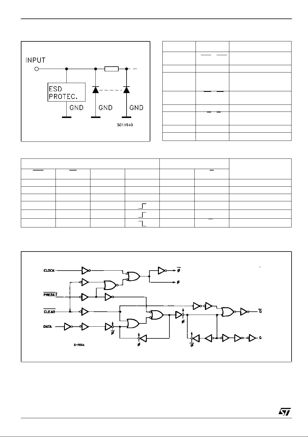
Figure 2: Input Equivalent Circuit Table 2: Pin Description
PIN N° SYMBOL NAME AND FUNCTION
1, 13 1CLR
2, 12 1D, 2D Data Inputs
3, 11 1CK, 2CK Clock Input
4, 10 1PR
5, 9 1Q, 2Q True Flip-Flop Outputs
6, 8 1Q
7 GND Ground (0V)
14 V
Table 3: Truth Table
, 2CLR
, 2PR Asynchronous Set - Direct
, 2Q Complement Flip-Flop
CC
Asynchronous Reset Direct Input
(LOW to HIGH, Edge
Triggered)
Input
Outputs
Positive Supply Voltage
INPUTS OUTPUTS
FUNCTION
CLR
PR DCKQ Q
LHXXLH CLEAR
H L X X H L PRESET
LLXXHH
HHL LH
HHH HL
HHX
X : Don’t Ca re
Q
n
Q
n
NO CHANGE
Figure 3: Logic Diagram
This logi c di agram has not be used to est i m ate propaga tion delays
2/14
74VHC74
Table 4: Absolute Maximum Ratings
Symbol Parameter Value Unit
V
V
V
I
I
OK
I
or I
I
CC
T
T
Absolute Maximum Ratings are those values beyond which damage to the device may occur. Functional operation under these conditions is
not implied
Table 5: Recommended Operating Conditions
Symbol Parameter Value Unit
V
V
V
T
dt/dv
Supply Voltage
CC
DC Input Voltage
I
DC Output Voltage -0.5 to VCC + 0.5
O
DC Input Diode Current
IK
DC Output Diode Current
DC Output Current
O
DC VCC or Ground Current
GND
Storage Temperature
stg
Lead Temperature (10 sec)
L
Supply Voltage
CC
Input Voltage
I
Output Voltage 0 to V
O
Operating Temperature
op
Input Rise and Fall Time (note 1) (V
(V
= 3.3 ± 0.3V)
CC
= 5.0 ± 0.5V)
CC
-0.5 to +7.0 V
-0.5 to +7.0 V
- 20 mA
± 20 mA
± 25 mA
± 50 mA
-65 to +150 °C
300 °C
2 to 5.5 V
0 to 5.5 V
CC
-55 to 125 °C
0 to 100
0 to 20
ns/V
V
V
1) VIN from 30 % t o 70% of V
CC
3/14
74VHC74
Table 6: DC Specifications
Symbol Parameter
V
V
V
High Level Input
IH
Voltage
V
Low Level Input
IL
Voltage
High Level Output
OH
Voltage
Low Level Output
OL
Voltage
I
Input Leakage
I
Current
I
Quiescent Supply
CC
Current
V
3.0 to
3.0 to
0 to
Test Condition Value
= 25°C
(V)
CC
T
A
Min. Typ. Max. Min. Max. Min. Max.
-40 to 85°C -55 to 125°C
2.0 1.5 1.5 1.5
5.5
0.7V
CC
0.7V
CC
0.7V
CC
2.0 0.5 0.5 0.5
5.5
2.0
3.0
4.5
3.0
4.5
2.0
3.0
4.5
3.0
4.5
VI = 5.5V or GND
5.5
V
5.5
IO=-50 µA
I
=-50 µA
O
=-50 µA
I
O
=-4 mA
I
O
=-8 mA
I
O
IO=50 µA
=50 µA
I
O
=50 µA
I
O
=4 mA
I
O
=8 mA
I
O
= VCC or GND
I
0.3V
CC
1.9 2.0 1.9 1.9
2.9 3.0 2.9 2.9
4.4 4.5 4.4 4.4
2.58 2.48 2.4
3.94 3.8 3.7
0.0 0.1 0.1 0.1
0.0 0.1 0.1 0.1
0.0 0.1 0.1 0.1
0.36 0.44 0.55
0.36 0.44 0.55
± 0.1 ± 1 ± 1 µA
22020µA
0.3V
CC
0.3V
CC
Unit
V
V
V
V
4/14
Table 7: AC Electrical Characteristics (Input tr = tf = 3ns)
Test Condition Value
= 25°C
Symbol Parameter
t
Propagation Delay
PLH
t
t
t
Time CK to Q or Q
PHL
Propagation Delay
PLH
Time PR
PHL
Q or Q
t
CK Pulse Width
W
HIGH or LOW
t
W
PR or CLR Pulse
or CLR to
Width LOW
t
Setup Time D to CK
s
HIGH or LOW
t
Hold Time D to CK
h
HIGH or LOW
MAX
Removal Time
or CLR to CK
PR
Maximum Clock
Frequency
t
REM
f
V
3.3
3.3
5.0
5.0
3.3
3.3
5.0
5.0
3.3
5.0
3.3
5.0
3.3
5.0
3.3
5.0
3.3
5.0
3.3
3.3
5.0
5.0
C
CC
(V)
L
(pF)
(*)
15 6.7 11.9 1.0 14.0 1.0 14.0
(*)
50 9.2 15.4 1.0 17.5 1.0 17.5
(**)
15 4.6 7.3 1.0 8.5 1.0 8.5
(**)
50 6.1 9.3 1.0 10.5 1.0 10.5
(*)
15 7.6 12.3 1.0 14.5 1.0 14.5
(*)
50 10.1 15.8 1.0 18.0 1.0 18.0
(**)
15 4.8 7.7 1.0 9.0 1.0 9.0
(**)
50 6.3 9.7 1.0 11.0 1.0 11.0
(*)
(**)
(*)
(**)
(*)
(**)
(*)
(**)
(*)
(**)
(*)
15 80 125 70 70
(*)
50 50 75 45 45
(**)
15 130 170 110 110
(**)
50 90 115 75 75
T
A
Min. Typ. Max. Min. Max. Min. Max.
74VHC74
-40 to 85°C -55 to 125°C
6.0 7.0 7.0
5.0 5.0 5.0
6.0 7.0 7.0
5.0 5.0 5.0
6.0 7.0 7.0
5.0 5.0 5.0
0.5 0.5 0.5
0.5 0.5 0.5
5.0 5.0 5.0
3.0 3.0 3.0
Unit
ns
ns
ns
ns
ns
ns
ns
MHz
(*) Voltage range is 3.3V ± 0.3V
(**) Voltage range is 5.0V ±
0.5V
Table 8: Capacitive Characteristics
Test Condition Value
= 25°C
Symbol Parameter
C
C
Input Capacitance
IN
Power Dissipation
PD
Capacitance
V
CC
(V)
5.0 7 10 10 10 pF
= 10MHz
5.0
f
IN
T
A
Min. Typ. Max. Min. Max. Min. Max.
25 pF
(note 1)
1) CPD is defined as the value of the IC’s internal equivalent capacitance which is calculated from the operating current consumption without
load. (R ef er to Test Circ ui t). Averag e operating current can be obtained by t he following equation. I
flip-flop)
-40 to 85°C -55 to 125°C
= CPD x VCC x fIN + ICC/2 (per
CC(opr)
Unit
5/14
 Loading...