

74VHC594
8 BIT SHIFT REGISTER
WITH OUTPUT REGISTER
■ HIGH SPEED: t
■ LOW POWER DISSIPATION:
I
= 4 µA (MAX.) at TA=25°C
CC
■ HIGH NOISE IMMUNITY:
V
= V
NIH
■ POWER DOWN PROTECTION ON INPUTS
■ SYMMETRICAL OUTPUT IMPEDANCE:
|I
OH
■ BALANCED PROPAGATION DELAYS:
t
PLH
■ OPERATING VOLTAGE RANGE:
V
CC
■ PIN AND FUNCTION COMPATIBLE WITH
NIL
| = IOL = 8 mA (MIN)
≅ t
PHL
(OPR) = 2V to 5.5V
= 4.2ns (TYP.) at VCC = 5V
PD
= 28% VCC (MIN.)
74 SERIES 594
■ IMPROVED LATCH-UP IMMUN ITY
■ LOW NOISE: V
= 0.8V (MAX.)
OLP
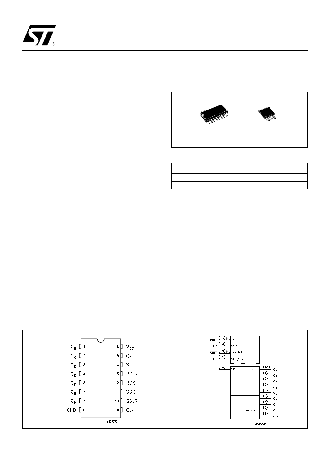
DESCRIPTION
The 74VHC594 is an high speed CMOS 8-BIT
SHIFT REGISTERS fabricated with sub-micron
silicon gate C
2
MOS technology.
This device contains an 8-bit serial-in, parallel-out
shift register that feeds an 8-bit D-type storage
register. Separate clocks and direct overriding
clear (SCLR,
RCLR) are provided for both the shift
register and the storage register.
TSSOPSOP
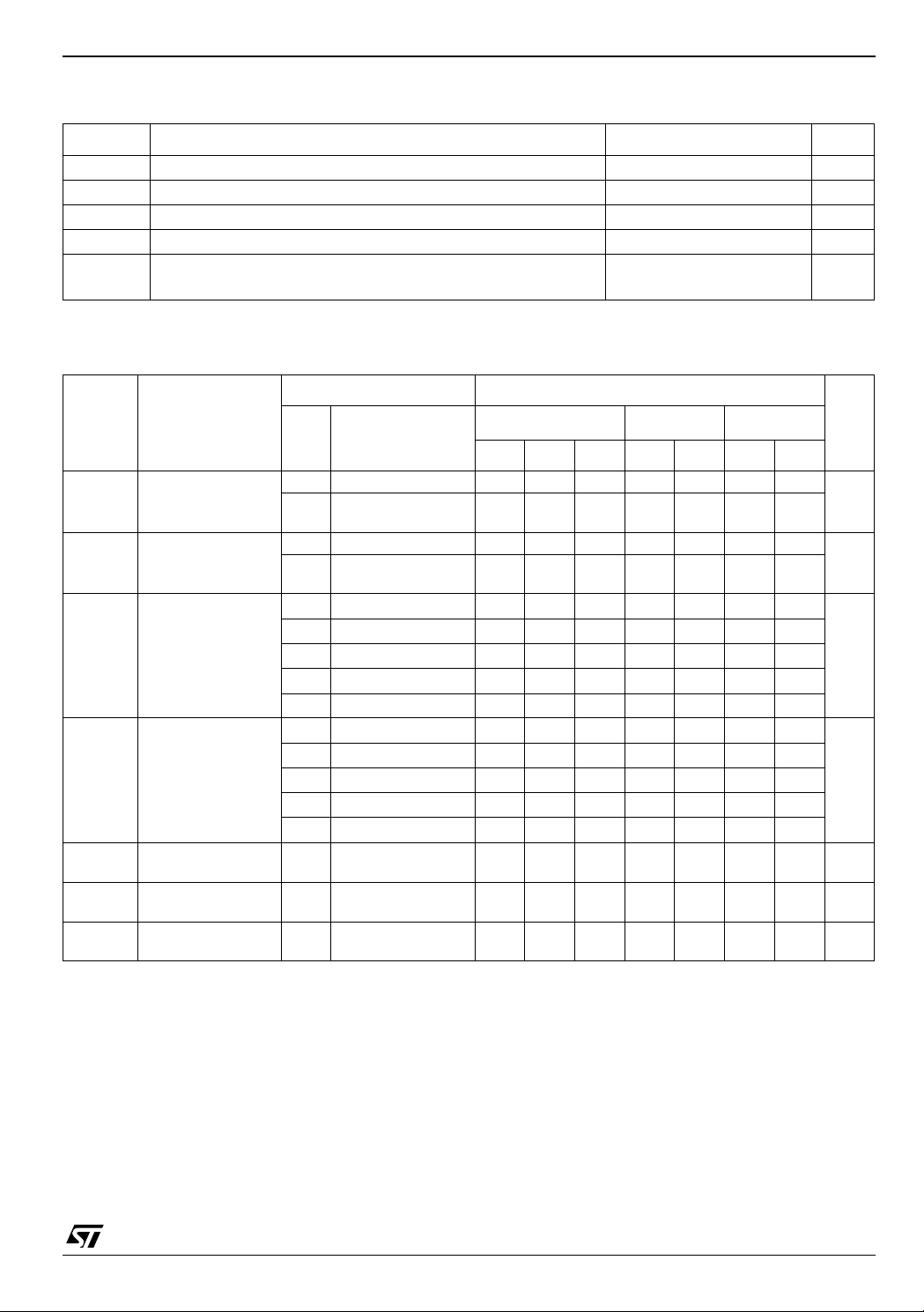
Table 1: Order Codes
PACKAGE T & R
SOP M74VHC594RMTR
TSSOP M74VHC594TTR
A serial (QH’) output is provided for cascading
purposes.
Both the shift register and storage
register use positive-edge triggered clocks. If the
clocks are connected together, the shift register
state will always be one c lock pulse a head of the
storage register.
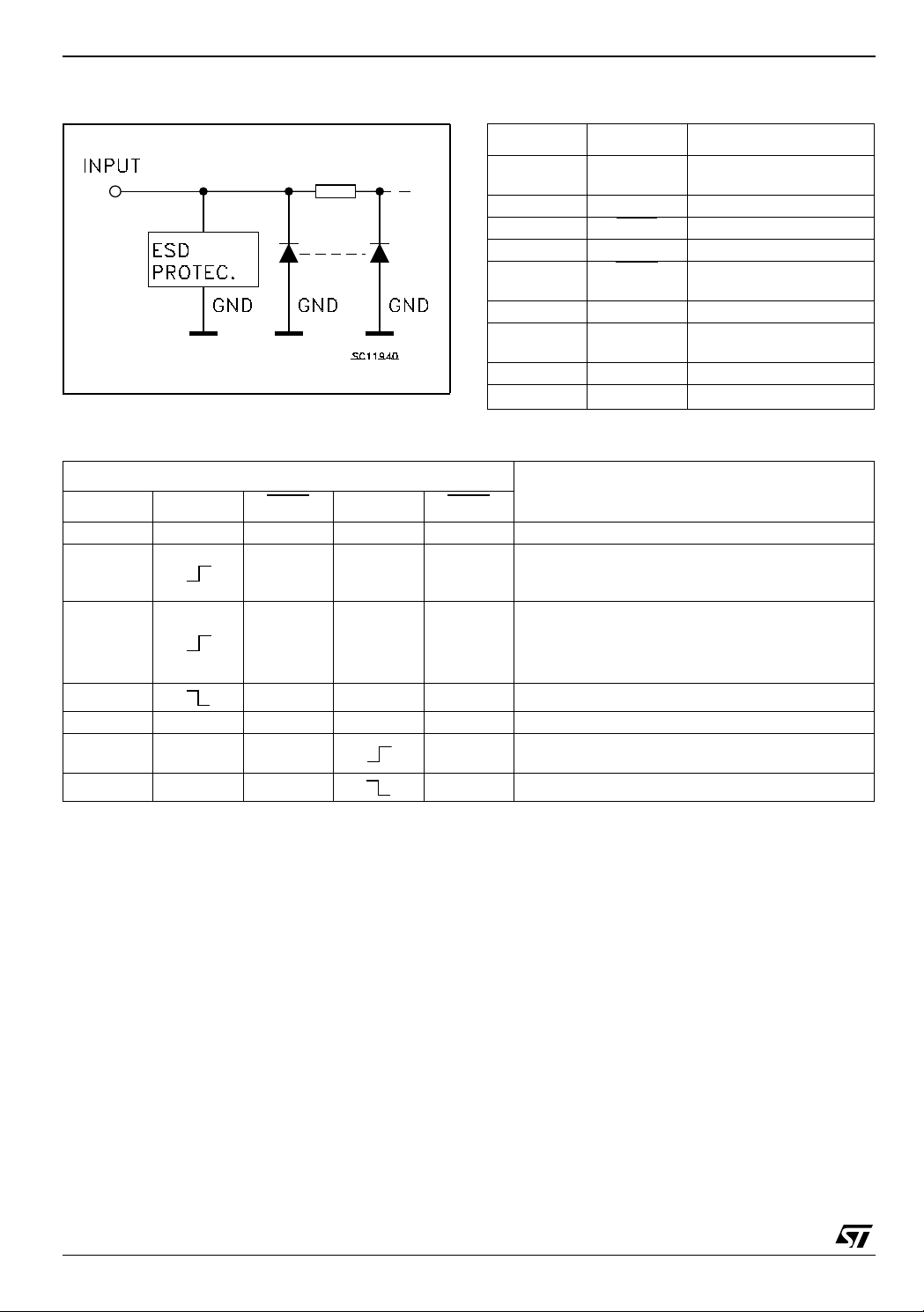
Power down protection is provided on all inputs
and 0 to 7V can be accepted on inputs with no
regard to the supply voltage. This device can be
used to interface 5V to 3V.
All inputs are equipped with protection circuits
against static discharge, giving them 2KV ESD
immunity and transient excess voltage.
Figure 1: Pin Connection An d I E C Logic Symbols
Rev. 5
1/14November 2004
74VHC594
Figure 2: Input Equivalent Circuit Table 2: Pin Description
PIN N° SYMBOL NAME AND FUNCTION
1, 2, 3, 4, 5,
6, 7, 15
9 QH’ Serial Data Output
10 SCLR
11 SCK Shift Register Clock Input
13 RCLR
14 SI Serial Data Input
12 RCK Storage Register Clock
8 GND Ground (0V)
16 V
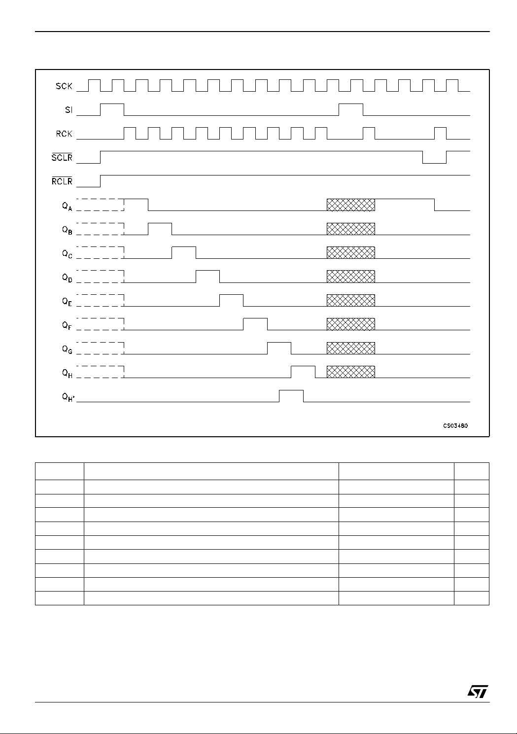
Table 3: Truth Table
QA to QH Data Outputs
Shift Register Clear Input
Storage Register Clear
Input
Input
CC
Positive Supply Voltage
INPUTS
SI SCK SCLR
X X L X X SHIFT REGISTER IS CLEAR
LHXX
HHXX
L H X X SHIFT REGISTER STATE IS NOT CHANGED
X X X X L STORAGE REGISTER IS CLEARED
XXX H
X X X H STORAGE REGISTER STATE IS NOT CHANGED
X: Don’t Care
RCK RCLR
FIRST STAGE OF SHIFT REGISTER GOES LOW
OTHER STAGES STORE THE DATA OF PREVI-
OUS STAGE, RESPECTIVELY
FIRST STAGE OF SHIFT REGISTER GOES HIGH
OTHER STAGES STORE THE DATA OF PREVI-
OUS STAGE, RESPECTIVELY
SHIFT REGISTER DATA IS STORED IN THE
OUTPUTS
STORAGE REGISTER
2/14
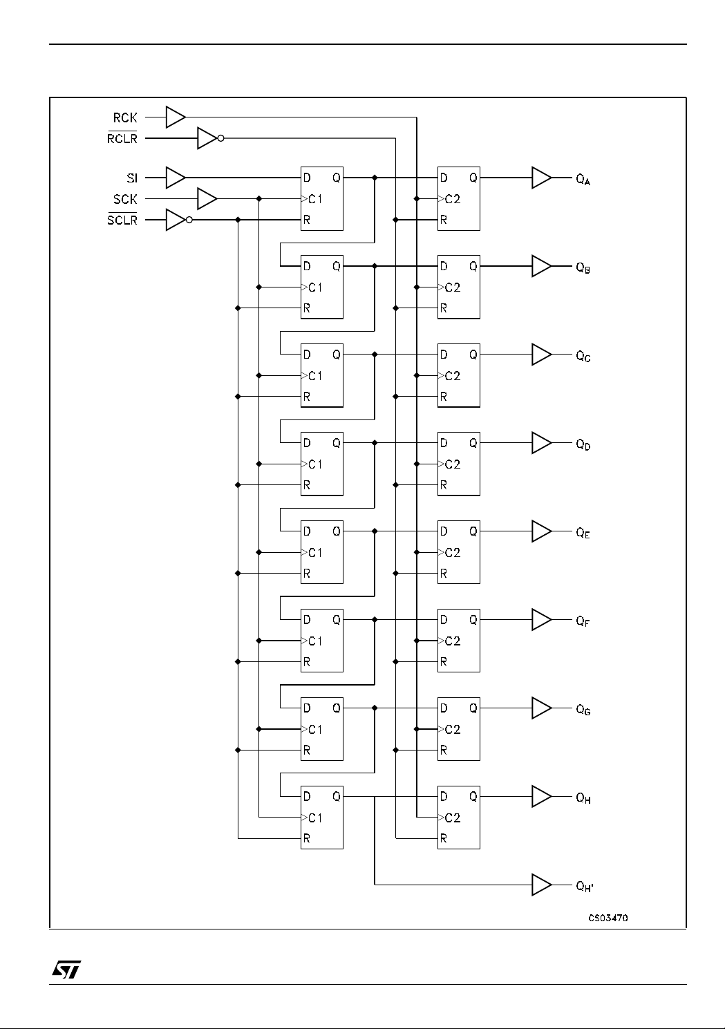
Figure 3: Logic Diagram
74VHC594
This logi c di agram has not be used to est i m ate propaga tion delays
3/14
74VHC594
Figure 4: Timing Chart
Table 4: Absolute Maximum Ratings
Symbol Parameter Value Unit
V
V
V
I
I
OK
I
or I
I
CC
T
T
Absolute Maximum Ratings are those values beyond which damage to the device may occur. Functional operation under these conditions is
not implied
4/14
Supply Voltage
CC
DC Input Voltage
I
DC Output Voltage -0.5 to VCC + 0.5
O
DC Input Diode Current
IK
DC Output Diode Current
DC Output Current
O
DC VCC or Ground Current
GND
Storage Temperature
stg
Lead Temperature (10 sec)
L
-0.5 to +7.0 V
-0.5 to +7.0 V
V
- 20 mA
± 20 mA
± 25 mA
± 50 mA
-65 to +150 °C
300 °C
74VHC594
Table 5: Recommended Operating Conditions
Symbol Parameter Value Unit
V
V
V
T
dt/dv
Supply Voltage
CC
Input Voltage
I
Output Voltage 0 to V
O
Operating Temperature
op
Input Rise and Fall Time (note 1) (V
(V
= 3.3 ± 0.3V)
CC
= 5.0 ± 0.5V)
CC
2 to 5.5 V
0 to 5.5 V
CC
-55 to 125 °C
0 to 100
0 to 20
V
ns/V
1) VI from 30 % t o 70% of V
CC
Table 6: DC Specifications
Symbol Parameter
V
V
V
High Level Input
IH
Voltage
V
Low Level Input
IL
Voltage
High Level Output
OH
Voltage
Low Level Output
OL
Voltage
Input Leakage
I
I
Current
Power Off Leakage
I
off
Current
I
Quiescent Supply
CC
Current
3.0 to
3.0 to
Test Condition Value
V
(V)
CC
T
A
Min. Typ. Max. Min. Max. Min. Max.
-40 to 85°C -55 to 125°C
= 25°C
2.0 1.5 1.5 1.5
5.5
0.7V
CC
0.7V
CC
0.7V
CC
2.0 0.5 0.5 0.5
5.5
2.0
3.0
4.5
3.0
4.5
2.0
3.0
4.5
3.0
4.5
0 to
5.5
0
5.5
IO=-50 µA
=-50 µA
I
O
I
=-50 µA
O
=-4 mA
I
O
=-8 mA
I
O
IO=50 µA
I
=50 µA
O
=50 µA
I
O
=4 mA
I
O
=8 mA
I
O
V
= 5.5V or GND
I
= 0 to 5V
V
I
= VCC or GND
V
I
0.3V
CC
1.9 2.0 1.9 1.9
2.9 3.0 2.9 2.9
4.4 4.5 4.4 4.4
2.58 2.48 2.4
3.94 3.8 3.7
0.0 0.1 0.1 0.1
0.0 0.1 0.1 0.1
0.0 0.1 0.1 0.1
0.36 0.44 0.55
0.36 0.44 0.55
± 0.1 ± 1 ± 1 µA
± 0.1 ± 5 ± 5 µA
44040µA
0.3V
CC
0.3V
CC
Unit
V
V
V
V
5/14
 Loading...