

74VHC574
OCTAL D-TYP E FLIP FLOP
WITH 3 STATE OUTPUTS NON INVERTING
■ HIGH SPEED:
■ f
■ LOW POWER DISSIPATION:
■ HIGH NOISE IMMUNITY:
■ POWER DOWN PROTECTION ON INPUTS
■ SYMMETRICAL OUTPUT IMPEDANCE:
■ BALANCED PROPAGATION DELAYS :
■ OPERATING VOLTAGE RANGE:
■ PIN AND FUNCTION COMPATIBLE WITH
= 180 MHz (TYP.) at VCC = 5V
MAX
I
= 4 µA (MAX.) at TA=25°C
CC
V
= V
NIH
|I
| = IOL = 8 mA (MIN)
OH
t
≅ t
PLH
V
(OPR) = 2V to 5.5V
CC
= 28% VCC (MIN.)
NIL
PHL
74 SERIES 574
■ IMPROVED LATCH-UP IMMUNIT Y
■ LOW NOISE: V
= 0.9V (MAX.)
OLP
DESCRIPTION
The 74VHC574 is an advanced high-speed
CMOS OCT AL D- TYP E FL I P FL O P wi th 3 S TAT E
OUTPUTS NON INVERTING fabricated with
sub-micron silicon gate and double-layer metal
wiring C
2
MOS technology.
These 8 bit D-Type flip-flop is controlled by a clock
input (CK) and an output enable input (OE
).
On the positive transition of the clock, the Q
outputs will be set to the logic states that were
setup at the D inputs.
While the (OE
) input is low, the 8 outputs will be in
a normal logic state (high or low logic level) and
TSSOPSOP
Table 1: Order Codes
PACKAGE T & R
SOP 74VHC574MTR
TSSOP 74VHC574TTR
while high level the outputs will be in a high
impedance state.
The Output control does not affect the internal
operation of flip flop; that is, the old data can be
retained or the new data can be entered even
while the outputs are off.
Power down protection is provided on all inputs
and 0 to 7V can be accepted on inputs with no
regard to the supply voltage. This device can be
used to interface 5V to 3V.
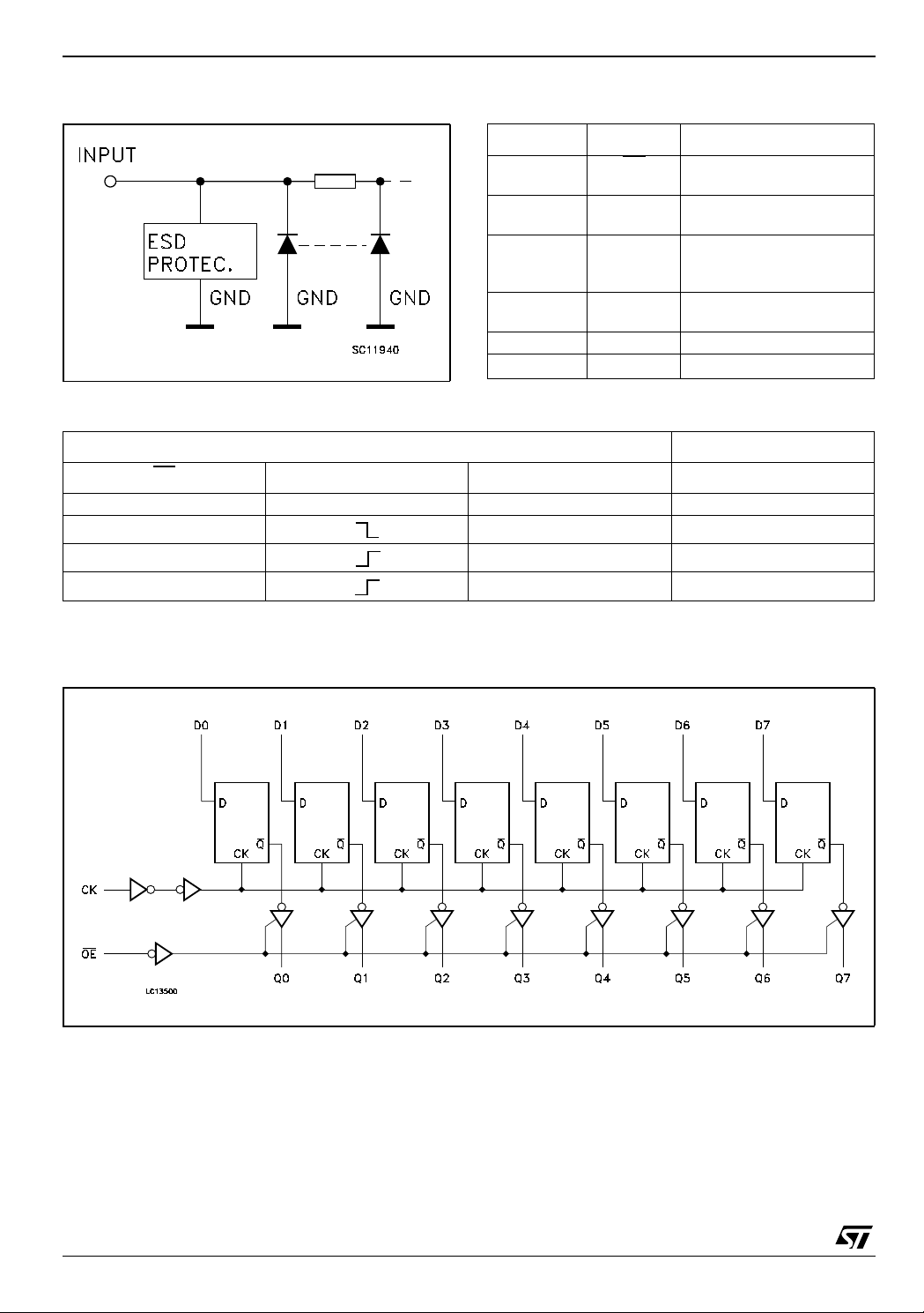
All inputs and outputs are equipped with
protection circuits against static disc harge, giving
them 2KV ESD immunity and transient excess
voltage.
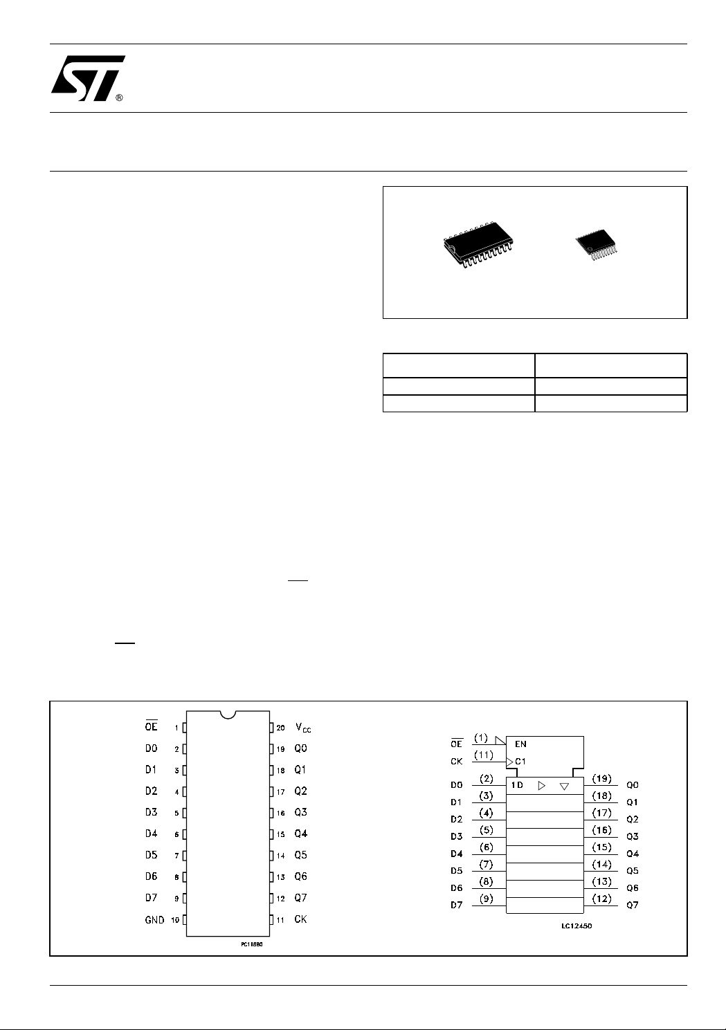
Figure 1: Pin Conne ction And IEC Logic Symbol s
Rev. 4
1/14November 2004
74VHC574
Figure 2: Input Equivalent Circuit Table 2: Pin Description
PIN N° SYMBOL NAME AND FUNCTION
Table 3: Truth Table
1OE
2, 3, 4, 5, 6,
7, 8, 9
12, 13, 14,
15, 16, 17,
18, 19
1 1 CK Clock Input (LOW-to-HIGH
10 GND Ground (0V)
20 V
INPUTS OUTPUT
D0 to D7 Data Inputs
Q0 to Q7 3-State Outputs
CC
3-State Output Enable
Input (Active LOW)
Edge Triggered)
Positive Supply Voltage
OE
HXXZ
L X NO CHANGE
LLL
LHH
X : Don’t Ca re
Z : High Impedance
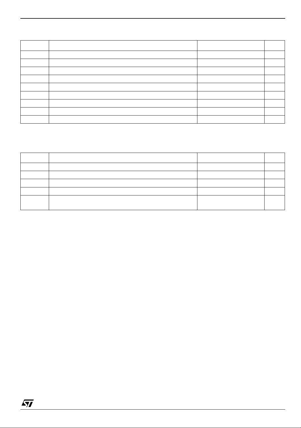
Figure 3: Logic Diagram
CK D Q
This logi c di agram has not be used to est i m ate propaga tion delays
2/14
74VHC574
Table 4: Absolute Maximum Ratings
Symbol Parameter Value Unit
V
V
V
I
I
OK
I
or I
I
CC
T
T
Absolute Maximum Ratings are those values beyond which damage to the device may occur. Functional operation under these conditions is
not implied
Table 5: Recommended Operating Conditions
Symbol Parameter Value Unit
V
V
V
T
dt/dv
Supply Voltage
CC
DC Input Voltage
I
DC Output Voltage -0.5 to VCC + 0.5
O
DC Input Diode Current
IK
DC Output Diode Current
DC Output Current
O
DC VCC or Ground Current
GND
Storage Temperature
stg
Lead Temperature (10 sec)
L
Supply Voltage
CC
Input Voltage
I
Output Voltage 0 to V
O
Operating Temperature
op
Input Rise and Fall Time (note 1) (V
(V
= 3.3 ± 0.3V)
CC
= 5.0 ± 0.5V)
CC
-0.5 to +7.0 V
-0.5 to +7.0 V
- 20 mA
± 20 mA
± 25 mA
± 75 mA
-65 to +150 °C
300 °C
2 to 5.5 V
0 to 5.5 V
CC
-55 to 125 °C
0 to 100
0 to 20
ns/V
V
V
1) VIN from 30 % t o 70% of V
CC
3/14
74VHC574
Table 6: DC Specifications
Symbol Parameter
V
V
V
High Level Input
IH
Voltage
V
Low Level Input
IL
Voltage
High Level Output
OH
Voltage
Low Level Output
OL
Voltage
I
High Impedance
OZ
Output Leakage
Current
Input Leakage
I
I
Current
I
Quiescent Supply
CC
Current
3.0 to
3.0 to
Test Condition Value
V
(V)
CC
T
A
Min. Typ. Max. Min. Max. Min. Max.
-40 to 85°C -55 to 125°C
= 25°C
2.0 1.5 1.5 1.5
5.5
0.7V
CC
0.7V
CC
0.7V
CC
2.0 0.5 0.5 0.5
5.5
2.0
3.0
4.5
3.0
4.5
2.0
3.0
4.5
3.0
4.5
5.5
VO = VCC or GND
0 to
V
5.5
V
5.5
IO=-50 µA
I
=-50 µA
O
=-50 µA
I
O
=-4 mA
I
O
=-8 mA
I
O
IO=50 µA
=50 µA
I
O
=50 µA
I
O
=4 mA
I
O
=8 mA
I
O
= VIH or V
V
I
= 5.5V or GND
I
= VCC or GND
I
IL
0.3V
CC
1.9 2.0 1.9 1.9
2.9 3.0 2.9 2.9
4.4 4.5 4.4 4.4
2.58 2.48 2.4
3.94 3.8 3.7
0.0 0.1 0.1 0.1
0.0 0.1 0.1 0.1
0.0 0.1 0.1 0.1
0.36 0.44 0.55
0.36 0.44 0.55
±0.25 ± 2.5 ± 2.5 µA
± 0.1 ± 1 ± 1 µA
44040µA
0.3V
CC
0.3V
CC
Unit
V
V
V
V
4/14
Table 7: AC Electrical Characteristics (Input tr = tf = 3ns)
Test Condition Value
Symbol Parameter
t
Propagation Delay
PLH
t
t
t
t
t
f
t
OSLH
t
OSHL
Time
PHL
CH to Q
Output Enable
PZL
Time
PZH
Output Disable
PLZ
Time
PHZ
t
Clock Pulse Width
w
HIGH or LOW
t
Setup Time D to CK
s
HIGH or LOW
t
Hold Time D to CK
h
HIGH or LOW
Maximum Clock
MAX
Frequency
Output to Output
Skew time (note 1)
V
3.3
3.3
5.0
5.0
3.3
3.3
5.0
5.0
3.3
3.3
3.3
5.0
3.3
5.0
3.3
5.0
3.3
3.3
5.0
5.0
3.3
5.0
C
CC
(V)
L
(pF)
(*)
15 8.5 13.2 1.0 15.5 1.0 15.5
(*)
50 11.0 16.7 1.0 19.0 1.0 19.0
(**)
15 5.6 8.6 1.0 10.0 1.0 10.0
(**)
50 7.1 10.6 1.0 12.0 1.0 12.0
(*)
15 8.2 12.8 1.0 15.0 1.0 15.0
(*)
50 10.7 16.3 1.0 18.5 1.0 18.5
(**)
15 5.9 9.0 1.0 10.5 1.0 10.5
(**)
50 7.4 11.0 1.0 12.5 1.0 12.5
(*)
50 11.0 15.0 1.0 17.0 1.0 17.0
(*)
50 7.1 10.1 1.0 11.5 1.0 11.5
(*)
(**)
(*)
(**)
(*)
(**)
(*)
15 80 125 65 65
(*)
50 50 75 45 45
(**)
15 130 180 110 110
(**)
50 85 115 75 75
(*)
50 1.5 1.5 1.5
(**)
50 1.0 1.0 1.0
T
A
Min. Typ. Max. Min. Max. Min. Max.
= 25°C
74VHC574
-40 to 85°C -55 to 125°C
5.0 5.0 5.0
5.0 5.0 5.0
3.5 3.5 3.5
3.5 3.5 3.5
1.5 1.5 1.5
1.5 1.5 1.5
Unit
ns
ns
ns
ns
ns
ns
MHz
ns
(*) Voltage range is 3.3V ± 0.3V
(**) Voltage range is 5.0V ±
Note 1: Parameter guaranteed by design. t
0.5V
soLH
= |t
pLHm
- t
pLHn
|, t
soHL
= |t
pHLm
- t
pHLn
|
Table 8: Capacitive Characteristics
Test Condition Value
= 25°C
Symbol Parameter
T
A
Min. Typ. Max. Min. Max. Min. Max.
C
C
C
Input Capacitance
IN
Output
OUT
Capacitance
Power Dissipation
PD
Capacitance
710 10 10pF
9pF
28 pF
(note 1)
1) CPD is defined as the value of the IC’s internal equivalent capacitance which is calculated from the operating current consumption without
load. (R ef er to Test Circ ui t). Averag e operating current can be obtained by t he following equation. I
Flip-Flop)
-40 to 85°C -55 to 125°C
= CPD x VCC x fIN + ICC/8 (per
CC(opr)
Unit
5/14
 Loading...