

74VHC373
OCTAL D-TYPE LATCH
WITH 3 STATE OUTPUTS NON INVERTING
■ HIGH SPEED: t
■ LOW POWER DISSIPATION:
I
= 4 µA (MAX.) at TA=25°C
CC
■ HIGH NOISE IMMUNITY:
V
= V
NIH
■ POWER DOWN PROTECTION ON INPUTS
■ SYMMETRICAL OUTPUT IMPEDANCE:
|I
OH
■ BALANCED PROPAGATION DELAYS:
t
PLH
■ OPERATING VOLTAGE RANGE:
V
CC
■ PIN AND FUNCTION COMPATIBLE WITH
NIL
| = IOL = 8 mA (MIN)
≅ t
PHL
(OPR) = 2V to 5.5V
= 5.0 ns (TYP.) at VCC = 5V
PD
= 28% VCC (MIN.)
74 SERIES 373
■ IMPROVED LATCH-UP IMMUNITY
■ LOW NOISE: V
= 0.9V (MAX.)
OLP
DESCRIPTION
The 74VHC373 is an advanced high-speed
CMOS OCTAL D-TYPE LATCH with 3 STATE
OUTPUTS NON INVERTING fabricated with
sub-micron silicon gate and double-layer metal
wiring C
2
MOS technology.
These 8 bit D-Type latch are controlled by a latch
enable input (LE) and an output enable input (OE
While the LE inputs is held a t a high level, the Q
outputs will follow the data input precisely. Wh en
the LE is taken low, the Q o utputs w ill be lat ched
TSSOPSOP
Table 1: Order Codes
PACKAGE T & R
SOP 74VHC373MTR
TSSOP 74VHC373TTR
precisely at the logic level of D in put data. While
the (OE
) input is low, the 8 outputs will be in a
normal logic state (high or low logic level) and
while (OE
) is in high level, the outputs will be in a
high impedance state.
Power down protection is provided on all inputs
and 0 to 7V can be accepted on inputs with no
regard to the supply voltage. This device can be
used to interface 5V to 3V.
All inputs and outputs are equipped with
).
protection circuits against static disc harge, giving
them 2KV ESD immunity and transient excess
voltage.
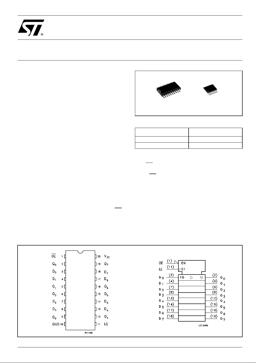
Figure 1: Pin Connection And IEC Logic Symbols
Rev. 4
1/14November 2004
74VHC373
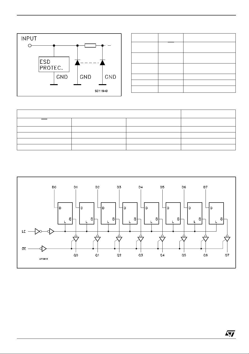
Figure 2: Input Equivalent Circuit Table 2: Pin Description
PIN N° SYMBOL NAME AND FUNCTION
Table 3: Truth Table
1OE
2, 5, 6, 9, 12,
D0 to D7 Data Inputs
15, 16,19
3, 4, 7, 8, 13,
Q0 to Q7 3-State Outputs
14, 17, 18
11 LE Latch Enable Input
10 GND Ground (0V)
20 V
CC
INPUTS OUTPUT
3 State Output Enable
Input (Active LOW)
Positive Supply Voltage
OE
LE D Q
HXXZ
LLXNO CHANGE*
LHLL
LHHH
X : Don’t Care
Z : High Impedance
* : Q Outputs are Latched at the time when the LE INPUT is taken low logic level
Figure 3: Logic Diagram
This logi c di agram has not be used to est i m ate propaga tion delays
2/14
74VHC373
Table 4: Absolute Maximum Ratings
Symbol Parameter Value Unit
V
V
V
I
I
OK
I
or I
I
CC
T
T
Absolute Maximum Ratings are those values beyond which damage to the device may occur. Functional operation under these conditions is
not implied
Table 5: Recommended Operating Conditions
Symbol Parameter Value Unit
V
V
V
T
dt/dv
Supply Voltage
CC
DC Input Voltage
I
DC Output Voltage -0.5 to VCC + 0.5
O
DC Input Diode Current
IK
DC Output Diode Current
DC Output Current
O
DC VCC or Ground Current
GND
Storage Temperature
stg
Lead Temperature (10 sec)
L
Supply Voltage
CC
Input Voltage
I
Output Voltage 0 to V
O
Operating Temperature
op
Input Rise and Fall Time (note 1) (V
(V
= 3.3 ± 0.3V)
CC
= 5.0 ± 0.5V)
CC
-0.5 to +7.0 V
-0.5 to +7.0 V
- 20 mA
± 20 mA
± 25 mA
± 75 mA
-65 to +150 °C
300 °C
2 to 5.5 V
0 to 5.5 V
CC
-55 to 125 °C
0 to 100
0 to 20
ns/V
V
V
1) VIN from 30 % t o 70% of V
CC
3/14
74VHC373
Table 6: DC Specifications
Symbol Parameter
V
V
V
High Level Input
IH
Voltage
V
Low Level Input
IL
Voltage
High Level Output
OH
Voltage
Low Level Output
OL
Voltage
I
High Impedance
OZ
Output Leakage
Current
Input Leakage
I
I
Current
I
Quiescent Supply
CC
Current
Test Condition Value
V
(V)
CC
T
A
Min. Typ. Max. Min. Max. Min. Max.
-40 to 85°C -55 to 125°C
= 25°C
2.0 1.5 1.5 1.5
3.0 to
5.5
0.7V
CC
0.7V
CC
0.7V
CC
2.0 0.5 0.5 0.5
3.0 to
5.5
2.0
3.0
4.5
3.0
4.5
2.0
3.0
4.5
3.0
4.5
5.5
0 to
5.5
5.5
IO=-50 µA
I
=-50 µA
O
=-50 µA
I
O
=-4 mA
I
O
=-8 mA
I
O
IO=50 µA
=50 µA
I
O
=50 µA
I
O
=4 mA
I
O
=8 mA
I
O
= VIH or V
V
I
IL
VO = VCC or GND
V
= 5.5V or GND
I
= VCC or GND
V
I
1.9 2.0 1.9 1.9
2.9 3.0 2.9 2.9
4.4 4.5 4.4 4.4
2.58 2.48 2.4
3.94 3.8 3.7
0.3V
CC
0.3V
CC
0.0 0.1 0.1 0.1
0.0 0.1 0.1 0.1
0.0 0.1 0.1 0.1
0.36 0.44 0.55
0.36 0.44 0.55
±0.25 ± 2.5 ± 2.5 µA
± 0.1 ± 1 ± 1 µA
44040µA
0.3V
CC
Unit
V
V
V
V
4/14
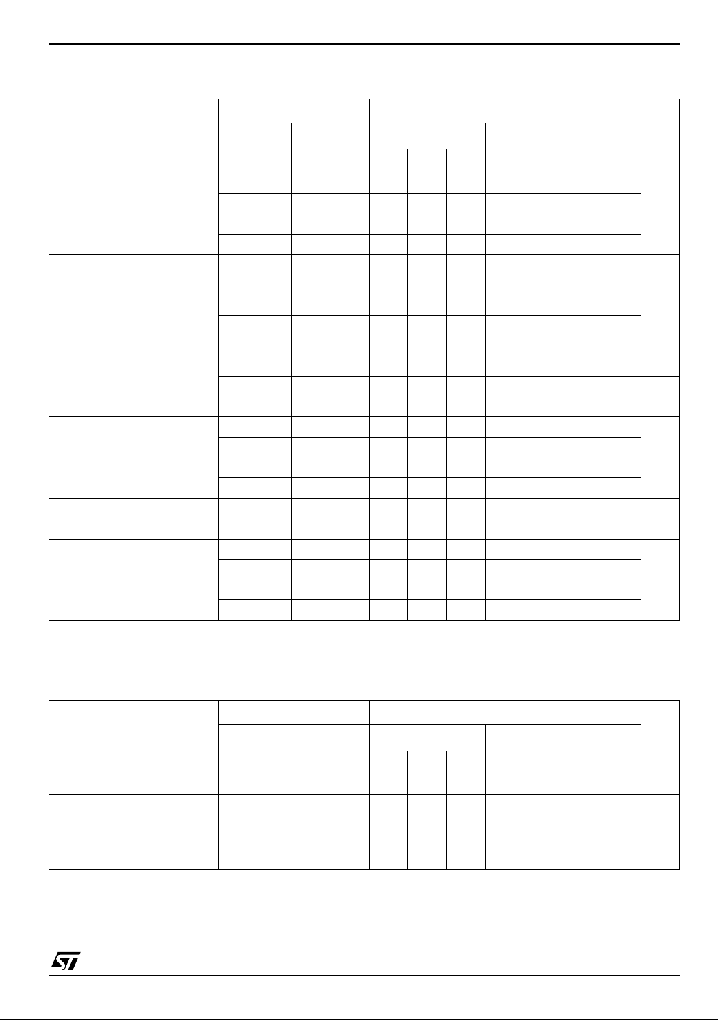
Table 7: AC Electrical Characteristics (Input tr = tf = 3ns)
Test Condition Value
Symbol Parameter
t
Propagation Delay
PLH
t
t
t
t
t
t
t
t
OSLH
t
OSHL
Time
PHL
LE to Q
Propagation Delay
PLH
Time
PHL
D to Q
Output Enable
PZL
Time
PZH
Output Disable
PLZ
Time
PHZ
t
Pulse Width (LE)
w
HIGH
Setup Time D to LE
t
s
HIGH or LOW
t
Setup Time D to LE
h
HIGH or LOW
Output to Output
Skew time (note 1)
V
3.3
3.3
5.0
5.0
3.3
3.3
5.0
5.0
3.3
3.3
5.0
5.0
3.3
5.0
3.3
5.0
3.3
5.0
3.3
5.0
3.3
5.0
C
CC
(V)
L
(pF)
(*)
15 7.0 11.0 1.0 13.0 1.0 13.0
(*)
50 9.5 14.5 1.0 16.5 1.0 16.5
(**)
15 4.9 7.2 1.0 8.5 1.0 8.5
(**)
50 6.4 9.2 1.0 10.5 1.0 10.5
(*)
15 7.3 11.4 1.0 13.5 1.0 13.5
(*)
50 9.8 14.9 1.0 17.0 1.0 17.0
(**)
15 5.0 7.2 1.0 8.5 1.0 8.5
(**)
50 6.5 9.2 1.0 10.5 1.0 10.5
(*)
15
(*)
50
(**)
15
(**)
50
(*)
50
(**)
50
(*)
(**)
(*)
(**)
(*)
(**)
(*)
50 1.5 1.5 1.5
(**)
50 1.0 1.0 1.0
R
L
R
L
R
L
R
L
R
L
R
L
= 1KΩ
= 1KΩ
= 1KΩ
= 1KΩ
= 1KΩ
= 1KΩ
T
A
Min. Typ. Max. Min. Max. Min. Max.
74VHC373
= 25°C
7.3 11.4 1.0 13.5 1.0 13.5
9.8 14.9 1.0 17.0 1.0 17.0
5.5 8.1 1.0 9.5 1.0 9.5
7.0 10.1 1.0 11.5 1.0 11.5
9.5 13.2 1.0 15.0 1.0 15.0
6.5 9.2 1.0 10.5 1.0 10.5
-40 to 85°C -55 to 125°C
5.0 5.0 5.0
5.0 5.0 5.0
4.0 4.0 4.0
4.0 4.0 4.0
1.0 1.0 1.0
1.0 1.0 1.0
Unit
ns
ns
ns
ns
ns
ns
ns
ns
ns
(*) Voltage range is 3.3V ± 0.3V
(**) Voltage range is 5.0V ±
Note 1 : Pa ram eter guara n t eed by design. t
0.5V
soLH
= |t
pLHm
- t
pLHn
|, t
soHL
= |t
pHLm
- t
pHLn
|
Table 8: Capacitive Characteristics
Test Condition Value
= 25°C
Symbol Parameter
T
A
Min. Typ. Max. Min. Max. Min. Max.
C
C
C
Input Capacitance
IN
Output
OUT
Capacitance
Power Dissipation
PD
Capacitance
710 10 10pF
9pF
15 pF
(note 1)
1) CPD is defined as the value of the IC’s internal equivalent capacitance which is calculated from the operating current consumption without
load. (Refer to Test Circuit). Average operating current can be obtained by the following equation. I
-40 to 85°C -55 to 125°C
= CPD x VCC x fIN + ICC/8 (per Latch)
CC(opr)
Unit
5/14
 Loading...