

ST 74VHC27 User Manual
74VHC27
TRIPLE 3-INPUT NOR GATE
■ HIGH SPEED: t
■ LOW POWER DISSIPATION:
I
= 2 µA (MAX.) at TA=25°C
CC
■ HIGH NOISE IMMUNITY:
V
= V
NIH
■ POWER DOWN PROTECTION ON INPUTS
■ SYMMETRICAL OUTPUT IMPEDANCE:
|I
OH
■ BALANCED PROPAGATION DELAYS:
t
PLH
■ OPERATING VOLTAGE RANGE:
V
CC
■ PIN AND FUNCTION COMPATIBLE WITH
NIL
| = IOL = 8mA (MIN)
≅ t
PHL
(OPR) = 2V to 5.5V
= 4.1 ns (TYP.) at VCC = 5V
PD
= 28% VCC (MIN.)
74 SERIES 27
■ IMPROVED LATCH-UP IMMUNITY
DESCRIPTION
The 74VHC27 is an advanced high-speed CMOS
TRIPLE 3-INPUT NOR GATE fabricated with
sub-micron silicon gate and double-layer metal
wiring C
2
MOS technology.
The internal circuit is composed of 3 stages
including buffer ou tput, whi ch provid es hig h no ise
immunity and stable output.
TSSOPSOP
Table 1: Order Codes
PACKAGE T & R
SOP 74VHC27MTR
TSSOP 74VHC27TTR
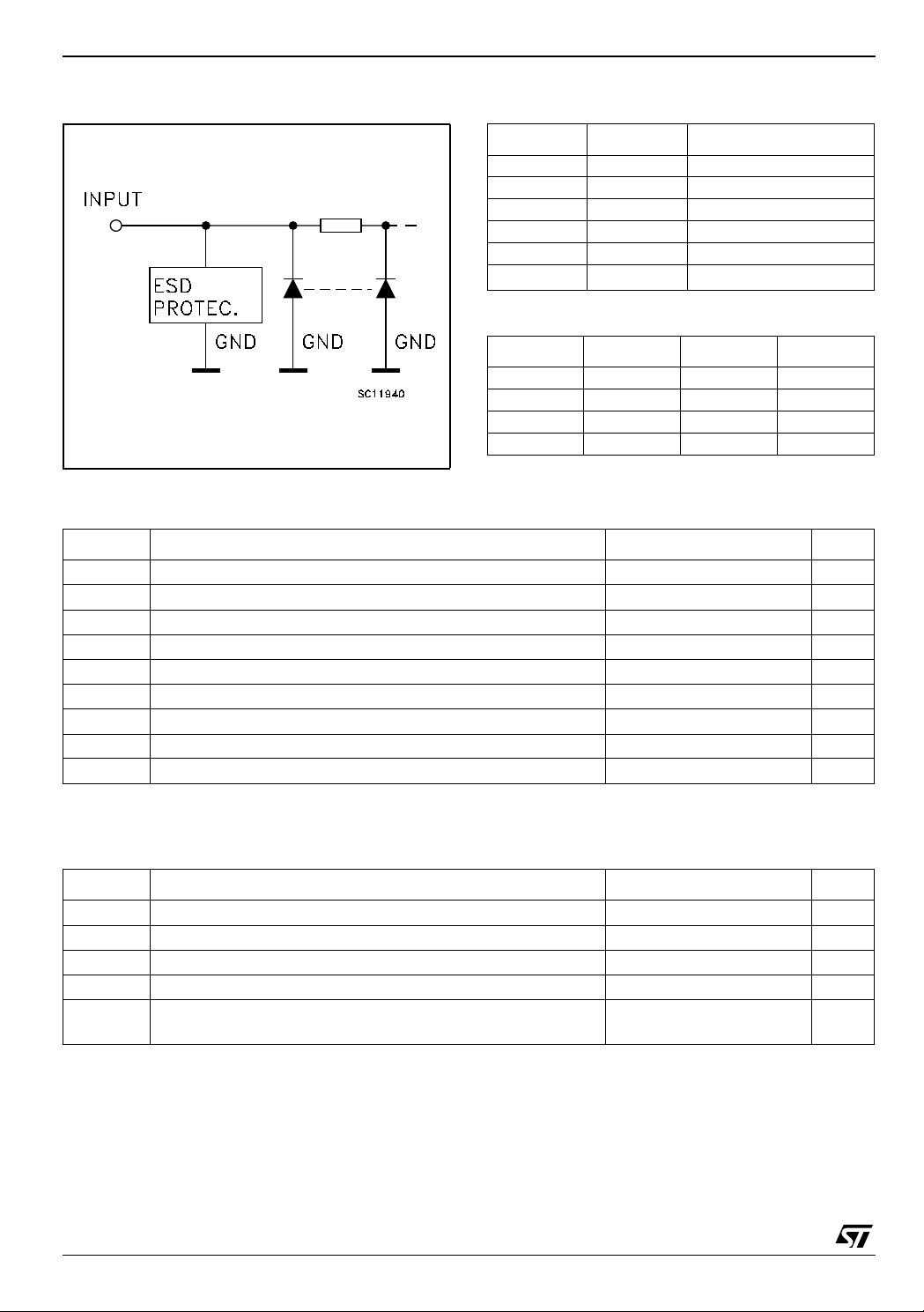
Power down protection is provided on all inputs
and 0 to 7V can be accepted on inputs with no
regard to the supply voltage. This device can be
used to interface 5V to 3V.
All inputs and outputs are equipped with
protection circuits against static disc harge, giving
them 2KV ESD immunity and transient excess
voltage.
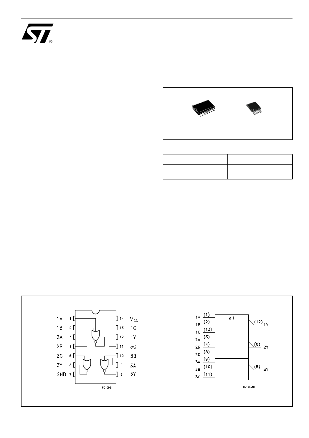
Figure 1: Pin Connection And IEC Logic Symbols
Rev. 4
1/10November 2004
74VHC27
Figure 2: Input Equivalent Circuit Table 2: Pin Description
PIN N° SYMBOL NAME AND FUNCTION
1, 3, 9 1A to 3A Data Inputs
2, 4, 10 1B to 3B Data Inputs
13, 5, 11 1C to 3C Data Inputs
12, 6, 8 1Y to 3Y Data Outputs
7 GND Ground (0V)
14
Table 3: Truth Table
ABCY
LLLH
HXXL
XHXL
XXHL
X : Don‘t Care
Table 4: Absolute Maximum Ratings
Symbol Parameter Value Unit
V
V
V
I
I
OK
I
or I
I
CC
T
T
Absolute Maximum Ratings are those values beyond which damage to the device may occur. Functional operation under these conditions is
not implied
Supply Voltage
CC
DC Input Voltage
I
DC Output Voltage -0.5 to VCC + 0.5
O
DC Input Diode Current
IK
DC Output Diode Current
DC Output Current
O
DC VCC or Ground Current
GND
Storage Temperature
stg
Lead Temperature (10 sec)
L
Table 5: Recommended Operating Conditions
V
CC
Positive Supply Voltage
-0.5 to +7.0 V
-0.5 to +7.0 V
- 20 mA
± 20 mA
± 25 mA
± 50 mA
-65 to +150 °C
300 °C
V
Symbol Parameter Value Unit
V
V
V
T
dt/dv
1) VIN from 30 % t o 70% of V
Supply Voltage
CC
Input Voltage
I
Output Voltage 0 to V
O
Operating Temperature
op
Input Rise and Fall Time (note 1) (V
(V
CC
= 3.3 ± 0.3V)
CC
= 5.0 ± 0.5V)
CC
2 to 5.5 V
0 to 5.5 V
CC
-55 to 125 °C
0 to 100
0 to 20
2/10
V
ns/V
Table 6: DC Specifications
Symbol Parameter
V
V
V
High Level Input
IH
Voltage
V
Low Level Input
IL
Voltage
High Level Output
OH
Voltage
Low Level Output
OL
Voltage
I
Input Leakage
I
Current
I
Quiescent Supply
CC
Current
V
(V)
2.0 1.5 1.5 1.5
3.0 to
5.5
2.0 0.5 0.5 0.5
3.0 to
5.5
2.0
3.0
4.5
3.0
4.5
2.0
3.0
4.5
3.0
4.5
0 to
5.5
5.5
Test Condition Value
= 25°C
T
CC
A
Min. Typ. Max. Min. Max. Min. Max.
0.7V
CC
0.3V
CC
IO=-50 µA
I
=-50 µA
O
=-50 µA
I
O
=-4 mA
I
O
=-8 mA
I
O
IO=50 µA
=50 µA
I
O
=50 µA
I
O
=4 mA
I
O
=8 mA
I
O
VI = 5.5V or GND
= VCC or GND
V
I
1.9 2.0 1.9 1.9
2.9 3.0 2.9 2.9
4.4 4.5 4.4 4.4
2.58 2.48 2.4
3.94 3.8 3.7
0.0 0.1 0.1 0.1
0.0 0.1 0.1 0.1
0.0 0.1 0.1 0.1
0.36 0.44 0.55
0.36 0.44 0.55
± 0.1 ± 1 ± 1 µA
22020µA
74VHC27
-40 to 85°C -55 to 125°C
0.7V
CC
0.3V
CC
0.7V
CC
0.3V
CC
Unit
V
V
V
V
Table 7: AC Electrical Characteristics (Input t
Test Condition Value
Symbol Parameter
t
Propagation Delay
PLH
PHL
Time
0.5V
t
(*) Voltage range is 3.3V ± 0.3V
(**) Voltage range is 5.0V ±
V
3.3
3.3
5.0
5.0
C
CC
(V)
L
(pF)
(*)
15 6.2 8.8 1.0 10.5 1.0 10.5
(*)
50 8.7 12.3 1.0 14.0 1.0 14.0
(**)
15 4.1 5.9 1.0 7.0 1.0 7.0
(**)
50 5.6 7.9 1.0 9.0 1.0 9.0
= tf = 3ns)
r
= 25°C
T
A
-40 to 85°C -55 to 125°C
Min. Typ. Max. Min. Max. Min. Max.
Unit
ns
3/10
 Loading...