

74VHC245
OCTAL BUS
TRANSCEIVER (3-STATE)
■ HIGH SPEED: t
■ LOW POWER DISSIPATION:
I
= 4 µA (MAX.) at TA=25°C
CC
■ HIGH NOISE IMMUNITY:
V
= V
NIH
■ POWER DOWN PROTECTION ON
NIL
= 4.0 ns (TYP.) at VCC = 5V
PD
= 28% VCC (MIN.)
CONTROL INPUTS
■ SYMMETRICAL OUTPUT IMPEDANCE:
|I
| = IOL = 8 mA (MIN)
OH
■ BALANCED PROPAGATION DELAYS:
t
≅ t
PLH
■ OPERATING VOLTAGE RANGE:
V
CC
■ PIN AND FUNCTION COMPATIBLE WITH
PHL
(OPR) = 2V to 5.5V
74 SERIES 245
■ IMPROVED LATCH-UP IMMUNITY
■ LOW NOISE: V
= 0.9V (MAX.)
OLP
DESCRIPTION
The 74VHC245 is an advanced high-speed
CMOS OCTAL BUS TRANSCEIVER (3-STATE)
fabricated with sub-micron silicon gate and
double-layer metal wiring C
2
MOS technology.
This IC is intended for two-way asynchronous
communication between data busses; the
TSSOPSOP
Table 1: Order Codes
PACKAGE T & R
SOP 74VHC245MTR
TSSOP 74VHC245TTR
direction of data transmission is determined by
DIR input. The enable input G
can be used to
disable the device so that the busses are
effectivel y isolated.
All inputs and outputs are equipped with
protection circuits against static disc harge, giving
them 2KV ESD immunity and transient excess
voltage.
All floating bus terminals during High Z State must
be held HIGH or LOW.
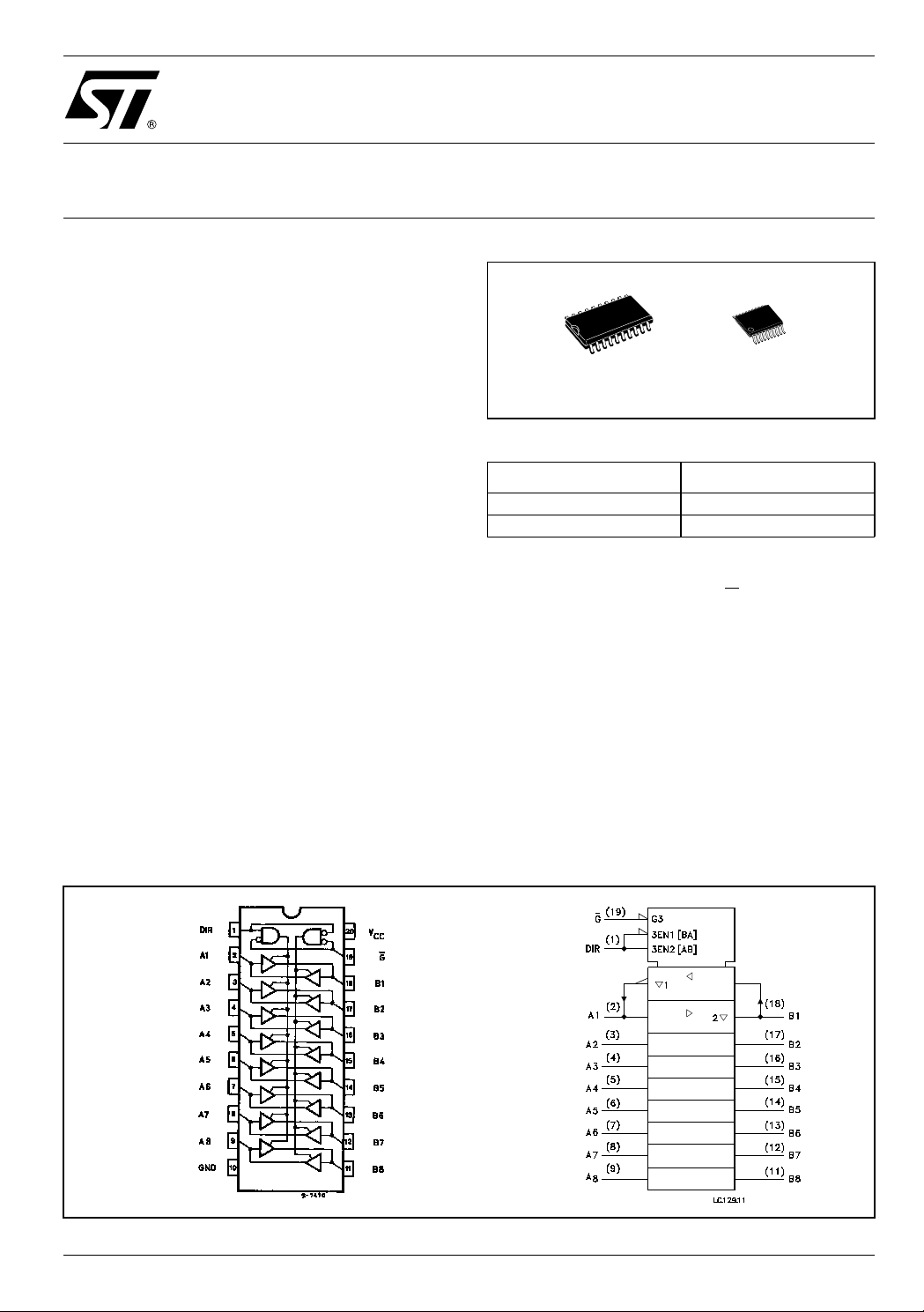
Figure 1: Pin Connection And IEC Logic Symbols
Rev. 6
1/12November 2004
74VHC245
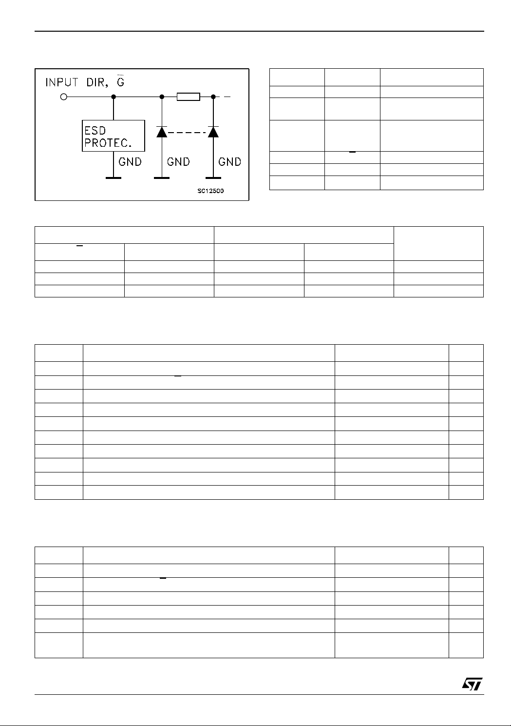
Figure 2: Input Equivalent Circuit Table 2: Pin Description
PIN N° SYMBOL NAME AND FUNCTION
1 DIR Directional Control
2, 3, 4, 5, 6,
7, 8, 9
18, 17, 16,
15, 14, 13,
12, 11
19 G
10 GND Ground (0V)
20 V
Table 3: Truth Table
A1 to A8 Data Inputs/Outputs
B1 to B8 Data Inputs/Outputs
Output Enable Input
CC
Positive Supply Voltage
INPUTS FUNCTION
OUTPUT
G
DIR A BUS B BUS
L L OUTPUT INPUT A = B
L H INPUT OUTPUT B = A
HXZZZ
X : Don‘t Care
Z : High Impedance
Table 4: Absolute Maximum Ratings
Symbol Parameter Value Unit
V
V
V
V
I
I
OK
I
or I
I
CC
T
T
Absolute Maximum Ratings are those values beyond which damage to the device may occur. Functional operation under these conditions is
not implied
Supply Voltage
CC
DC Input Voltage (DIR, G)
I
Bus I/O Voltage -0.5 to VCC + 0.5
I/O
DC Output Voltage -0.5 to VCC + 0.5
O
DC Input Diode Current
IK
DC Output Diode Current
DC Output Current
O
DC VCC or Ground Current
GND
Storage Temperature
stg
Lead Temperature (10 sec)
L
-0.5 to +7.0 V
-0.5 to +7.0 V
V
V
- 20 mA
± 20 mA
± 25 mA
± 75 mA
-65 to +150 °C
300 °C
Table 5: Recommended Operating Conditions
Symbol Parameter Value Unit
V
V
V
V
T
dt/dv
1) VIN from 30 % t o 70% of V
Supply Voltage
CC
Input Voltage (DIR, G)
I
Bus I/O Voltage 0 to V
I/O
Output Voltage 0 to V
O
Operating Temperature
op
Input Rise and Fall Time (note 1) (V
(V
CC
= 3.3 ± 0.3V)
CC
= 5.0 ± 0.5V)
CC
2 to 5.5 V
0 to 5.5 V
CC
CC
-55 to 125 °C
0 to 100
0 to 20
2/12
V
V
ns/V
Table 6: DC Specifications
Symbol Parameter
V
V
V
High Level Input
IH
Voltage
V
Low Level Input
IL
Voltage
High Level Output
OH
Voltage
Low Level Output
OL
Voltage
I
High Impedance
OZ
Output Leakage
Current
Input Leakage
I
I
Current
I
Quiescent Supply
CC
Current
74VHC245
Test Condition Value
= 25°C
T
V
(V)
CC
A
Min. Typ. Max. Min. Max. Min. Max.
2.0 1.5 1.5 1.5
3.0 to
5.5
0.7V
CC
2.0 0.5 0.5 0.5
3.0 to
5.5
2.0
3.0
4.5
3.0
4.5
2.0
3.0
4.5
3.0
4.5
5.5
0 to
5.5
5.5
IO=-50 µA
I
=-50 µA
O
=-50 µA
I
O
=-4 mA
I
O
=-8 mA
I
O
IO=50 µA
=50 µA
I
O
=50 µA
I
O
=4 mA
I
O
=8 mA
I
O
= VIH or V
V
I
IL
VO = VCC or GND
V
= 5.5V or GND
I
= VCC or GND
V
I
1.9 2.0 1.9 1.9
2.9 3.0 2.9 2.9
4.4 4.5 4.4 4.4
2.58 2.48 2.4
3.94 3.8 3.7
0.3V
0.0 0.1 0.1 0.1
0.0 0.1 0.1 0.1
0.0 0.1 0.1 0.1
±0.25 ± 2.5 ± 2.5 µA
-40 to 85°C -55 to 125°C
CC
0.7V
CC
0.3V
CC
0.7V
CC
0.36 0.44 0.55
0.36 0.44 0.55
± 0.1 ± 1 ± 1 µA
44040µA
0.3V
CC
Unit
V
V
V
V
3/12
74VHC245
Table 7: AC Electrical Characteristics (Input tr = tf = 3ns)
Test Condition Value
Symbol Parameter
t
Propagation Delay
PLH
t
t
t
t
t
t
OSLH
t
OSHL
Time
PHL
Output Disable
PZL
Time
PZH
PLZ
Output Enable
PHZ
Time
Output to Output
Skew time (note 1)
V
3.3
3.3
5.0
5.0
3.3
3.3
5.0
5.0
3.3
5.0
3.3
5.0
C
CC
(V)
L
(pF)
(*)
15 5.8 8.4 1.0 10.0 1.0 10.0
(*)
50 8.3 11.9 1.0 13.5 1.0 13.5
(**)
15 4.0 5.5 1.0 6.5 1.0 6.5
(**)
50 5.5 7.5 1.0 8.5 1.0 8.5
(*)
15
(*)
50
(**)
15
(**)
50
(*)
50
(**)
50
(*)
50 1.5 1.5 1.5
(**)
50 1.0 1.0 1.0
R
L
R
L
R
L
R
L
R
L
R
L
= 1KΩ
= 1KΩ
= 1KΩ
= 1KΩ
= 1KΩ
= 1KΩ
T
Min. Typ. Max. Min. Max. Min. Max.
= 25°C
A
-40 to 85°C -55 to 125°C
8.5 13.2 1.0 15.5 1.0 15.5
11.0 16.7 1.0 19.0 1.0 19.0
5.8 8.5 1.0 10.0 1.0 10.0
7.3 10.6 1.0 12.0 1.0 12.0
11.5 15.8 1.0 18.0 1.0 18.0
7.0 9.7 1.0 11.0 1.0 11.0
Unit
ns
ns
ns
ns
(*) Voltage range is 3.3V ± 0.3V
(**) Voltage range is 5.0V ±
Note 1: Parameter guaranteed by design. t
0.5V
soLH
= |t
pLHm
- t
pLHn
|, t
soHL
= |t
pHLm
- t
pHLn
|
Table 8: Capacitive Characteristics
Test Condition Value
= 25°C
Symbol Parameter
T
A
Min. Typ. Max. Min. Max. Min. Max.
C
C
C
Input Capacitance
IN
Output
I/O
Capacitance
Power Dissipation
PD
Capacitance
410 10 10pF
8pF
21 pF
(note 1)
1) CPD is defined as the value of the IC’s internal equivalent capacitance which is calculated from the operating current consumption without
load. (Refer to Test Circuit). Average operating current can be obtained by the following equation. I
-40 to 85°C -55 to 125°C
= CPD x VCC x fIN + ICC/8 (per c ircuit )
CC(opr)
Unit
4/12
 Loading...