

74VHC174
HEX D-TYPE FLIP FLOP WITH CLEAR
■ HIGH SPEED:
f
= 175MHz (TYP.) at VCC = 5V
MAX
■ LOW POWER DISSIPATION:
I
= 4 µA (MAX.) at TA=25°C
CC
■ HIGH NOISE IMMUNITY:
V
= V
NIH
■ POWER DOWN PROTECTION ON INPUTS
■ SYMMETRICAL OUTPUT IMPEDANCE:
|I
| = IOL = 8 mA (MIN)
OH
■ BALANCED PROPAGATION DELAYS:
t
≅ t
PLH
■ OPERATING VOLTAGE RANGE:
V
(OPR) = 2V to 5.5V
CC
■ PIN AND FUNCTION COMPATIBLE WITH
= 28% VCC (MIN.)
NIL
PHL
74 SERIES 174
■ IMPROVED LATCH-UP IMMUNITY
■ LOW NOISE: V
= 0.8V (MAX.)
OLP
DESCRIPTION
The 74VHC174 is an advanced high-speed
CMOS HEX D-TYPE FLIP FLOP WITH CLEAR
fabricated with sub-micron silicon gate and
double-layer metal wiring C
2
MOS technology.
Information signals applied to D inputs are
transferred to the Q o utputs on the positive going
edge of the clock pulse.
TSSOPSOP
Table 1: Order Codes
PACKAGE T & R
SOP 74VHC174MTR
TSSOP 74VHC174TTR
When the CLE AR
input is held low, the Q outputs
are held low independently of the other inputs.
Power down protection is provided on all inputs
and 0 to 7V can be accepted on inputs with no
regard to the supply voltage. This device can be
used to interface 5V to 3V.
All inputs and outputs are equipped with
protection circuits against static disc harge, giving
them 2KV ESD immunity and transient excess
voltage.
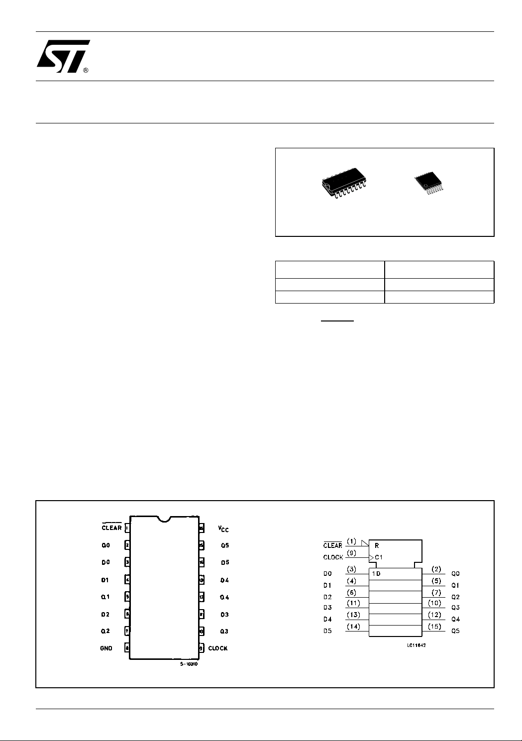
Figure 1: Pi n C onnect ion And I E C Logic Sym bols
Rev. 4
1/14November 2004
74VHC174
Figure 2: Input Equivalent Circuit Table 2: Pin Description
PIN N° SYMBOL NAME AND FUNCTION
Table 3: Truth Ta ble
1CLEAR
2, 5, 7, 10,
12, 15
3, 4, 6, 11,
13, 14
9 CLOCK Clock Input (LOW-to-HIGH,
8 GND Ground (0V)
16 V
Q0 to Q5 Flip-Flop Outputs
D0 to D5 Data Inputs
CC
Asynchronous Maste r
Reset (Active LOW)
Edge Triggered)
Positive Supply Voltage
CLEAR
L X X L CLEAR
HL L
HH H
HX
X : Don’t Care
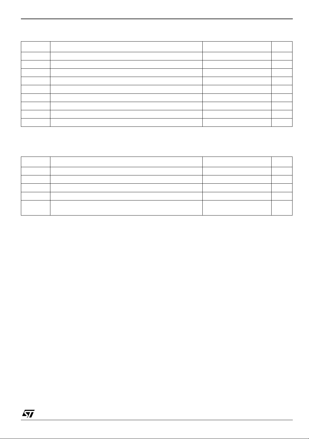
Figure 3: Logic Diagram
INPUTS OUTPUTS
DCLOCKQ
Q
n
FUNCTION
NO CHANGE
This log i c diagram has not to be used to es timate pro pagation del ays
2/14
74VHC174
Table 4: Absolute Maximum Ratings
Symbol Parameter Value Unit
V
V
V
I
I
OK
I
or I
I
CC
T
T
Absolute Maximum Ratings are those values beyond which damage to the device may occur. Functional operation under these conditions is
not implied
Table 5: Recommended Operating Conditions
Symbol Parameter Value Unit
V
V
V
T
dt/dv
Supply Voltage
CC
DC Input Voltage
I
DC Output Voltage -0.5 to VCC + 0.5
O
DC Input Diode Current
IK
DC Output Diode Current
DC Output Current
O
DC VCC or Ground Current
GND
Storage Temperature
stg
Lead Temperature (10 sec)
L
Supply Voltage
CC
Input Voltage
I
Output Voltage 0 to V
O
Operating Temperature
op
Input Rise and Fall Time (note 1) (V
(V
= 3.3 ± 0.3V)
CC
= 5.0 ± 0.5V)
CC
-0.5 to +7.0 V
-0.5 to +7.0 V
- 20 mA
± 20 mA
± 25 mA
± 50 mA
-65 to +150 °C
300 °C
2 to 5.5 V
0 to 5.5 V
CC
-55 to 125 °C
0 to 100
0 to 20
ns/V
V
V
1) VIN from 30 % t o 70% of V
CC
3/14
74VHC174
Table 6: DC Specifications
Symbol Parameter
V
V
V
High Level Input
IH
Voltage
V
Low Level Input
IL
Voltage
High Level Output
OH
Voltage
Low Level Output
OL
Voltage
I
Input Leakage
I
Current
I
Quiescent Supply
CC
Current
3.0 to
3.0 to
Test Condition Value
V
(V)
CC
T
A
Min. Typ. Max. Min. Max. Min. Max.
-40 to 85°C -55 to 125°C
= 25°C
2.0 1.5 1.5 1.5
5.5
0.7V
CC
0.7V
CC
0.7V
CC
2.0 0.5 0.5 0.5
5.5
2.0
3.0
4.5
3.0
4.5
2.0
3.0
4.5
3.0
4.5
0 to
VI = 5.5V or GND
5.5
V
5.5
IO=-50 µA
I
=-50 µA
O
=-50 µA
I
O
=-4 mA
I
O
=-8 mA
I
O
IO=50 µA
=50 µA
I
O
=50 µA
I
O
=4 mA
I
O
=8 mA
I
O
= VCC or GND
I
0.3V
CC
1.9 2.0 1.9 1.9
2.9 3.0 2.9 2.9
4.4 4.5 4.4 4.4
2.58 2.48 2.4
3.94 3.8 3.7
0.0 0.1 0.1 0.1
0.0 0.1 0.1 0.1
0.0 0.1 0.1 0.1
0.36 0.44 0.55
0.36 0.44 0.55
± 0.1 ± 1 ± 1 µA
44040µA
0.3V
CC
0.3V
CC
Unit
V
V
V
V
4/14
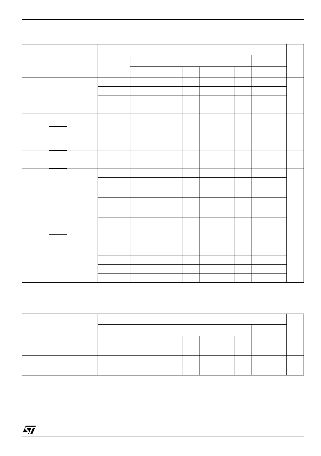
Table 7: AC Electrical Characteristics (Input tr = tf = 3ns)
Test Condition Value
Symbol Parameter
t
Propagation Delay
PLH
t
t
Time
PHL
CLOCK to Q
Propagation Delay
PHL
Time
CLEAR
t
CLEAR Pulse
W
Width LOW
t
CLEAR Pulse
W
Width HIGH or
to Q
LOW
t
Setup Time D to
s
CLOCK, HIGH or
LOW
t
Hold Time D to
h
CLOCK, HIGH or
LOW
t
REM
f
MAX
Recovery Time
to CLOCK
CLEAR
Maximum Clock
Frequency
V
3.3
3.3
5.0
5.0
3.3
3.3
5.0
5.0
3.3
5.0
3.3
5.0
3.3
5.0
3.3
5.0
3.3
5.0
3.3
3.3
5.0
5.0
C
CC
(V)
L
(pF)
(*)
15 5.8 11.0 1.0 13.0 1.0 13.0
(*)
50 7.5 14.5 1.0 16.5 1.0 16.5
(**)
15 4.1 7.2 1.0 8.5 1.0 8.5
(**)
50 5.5 9.2 1.0 10.5 1.0 10.5
(*)
15 7.4 11.4 1.0 13.5 1.0 13.5
(*)
50 9.9 14.9 1.0 17.0 1.0 17.0
(**)
15 5.1 7.6 1.0 9.0 1.0 9.0
(**)
50 6.6 9.6 1.0 11.0 1.0 11.0
(*)
(**)
(*)
(**)
(*)
(**)
(*)
(**)
(*)
(**)
(*)
15 95 150 80 80
(*)
50 55 85 50 50
(**)
15 130 175 110 110
(**)
50 90 120 80 80
T
A
Min. Typ. Max. Min. Max. Min. Max.
= 25°C
74VHC174
-40 to 85°C -55 to 125°C
5.0 5.0 5.0
5.0 5.0 5.0
5.0 5.0 5.0
5.0 5.0 5.0
5.0 6.0 6.0
4.5 4.5 4.5
0.0 0.0 0.0
0.5 0.5 0.5
3.0 3.0 3.0
2.5 2.5 2.5
Unit
ns
ns
ns
ns
ns
ns
ns
MHz
(*) Voltage range is 3.3V ± 0.3V
(**) Voltage range is 5.0V ±
0.5V
Table 8: Capacitive Characteristics
Test Condition Value
= 25°C
Symbol Parameter
T
A
Min. Typ. Max. Min. Max. Min. Max.
C
C
Input Capacitance
IN
Power Dissipation
PD
Capacitance
610 10 10pF
15 pF
(note 1)
1) CPD is defined as the value of the IC’s internal equivalent capacitance which is calculated from the operating current consumption without
load. (R ef er to Test Circ ui t). Averag e operating current can be obtained by t he following equation. I
Flip-Flop)
-40 to 85°C -55 to 125°C
= CPD x VCC x fIN + ICC/6 (per
CC(opr)
Unit
5/14
 Loading...