

74VHC157
QUAD 2 CHANNEL MULTIPLEXER
■ HIGH SPEED: t
■ LOW POWER DISSIPATION:
I
= 4 µA (MAX.) at TA=25°C
CC
■ HIGH NOISE IMMUNITY:
V
= V
NIH
■ POWER DOWN PROTECTION ON INPUTS
■ SYMMETRICAL OUTPUT IMPEDANCE:
|I
OH
■ BALANCED PROPAGATION DELAYS:
t
PLH
■ OPERATING VOLTAGE RANGE:
V
CC
■ PIN AND FUNCTION COMPATIBLE WITH
NIL
| = IOL = 8 mA (MIN)
≅ t
PHL
(OPR) = 2V to 5.5V
= 4.1 ns (TYP.) at VCC = 5V
PD
= 28% VCC (MIN.)
74 SERIES 157
■ IMPROVED LATCH-UP IMMUNITY
■ LOW NOISE: V
= 0.8V (MAX.)
OLP
DESCRIPTION
The 74VHC157 is an advanced high-speed
CMOS QUAD 2-CHANNEL MULTIPLEXER
fabricated with sub-micron silicon gate and
double-layer metal wiring C
2
MOS technology.
It consists of fo ur 2-input digital multiplexer with
common select and strobe inputs. It is a
non-inverting multiplexer. When the STROBE
TSSOPSOP
Table 1: Order Codes
PACKAGE T & R
SOP 74VHC157MTR
TSSOP 74VHC157TTR
input is held high selection of data is inhibited and
all the outputs become low. The SELECT
decoding determines whether the A or B inputs
get routed to their corresponding Y outputs.
Power down protection is provided on all inputs
and 0 to 7V can be accepted on inputs with no
regard to the supply voltage. This device can be
used to interface 5V t o 3V. All inputs and outputs
are equipped with protection circuits against static
discharge, giving them 2KV ESD immunity and
transient excess voltage.
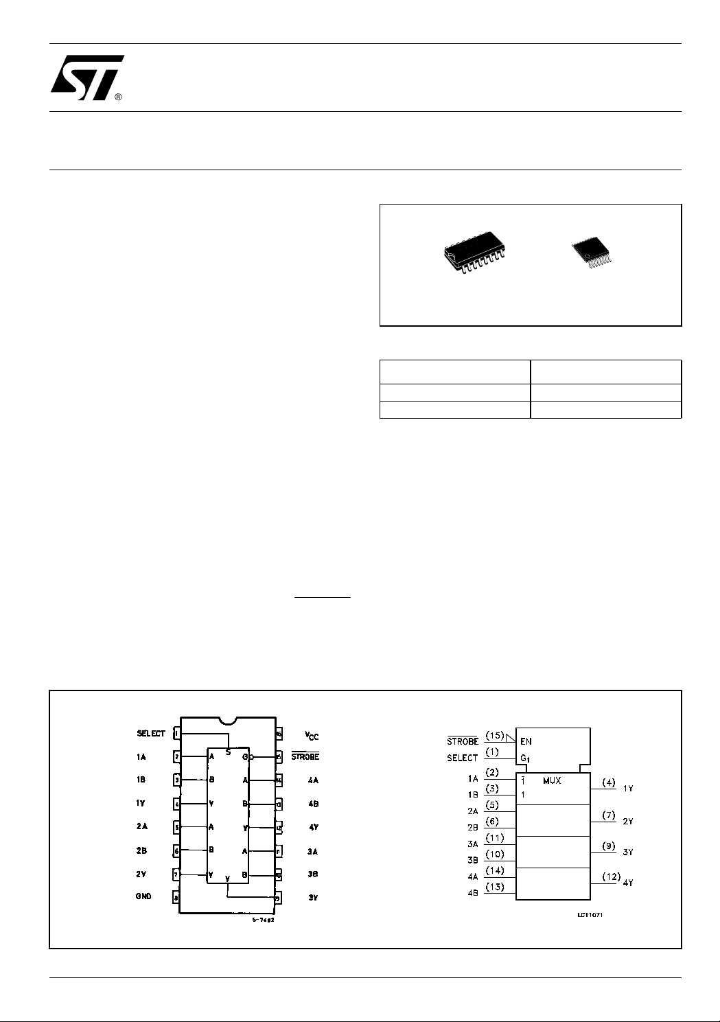
Figure 1: Pin Connection And IEC Logic Symbols
Rev. 4
1/12November 2004
74VHC157
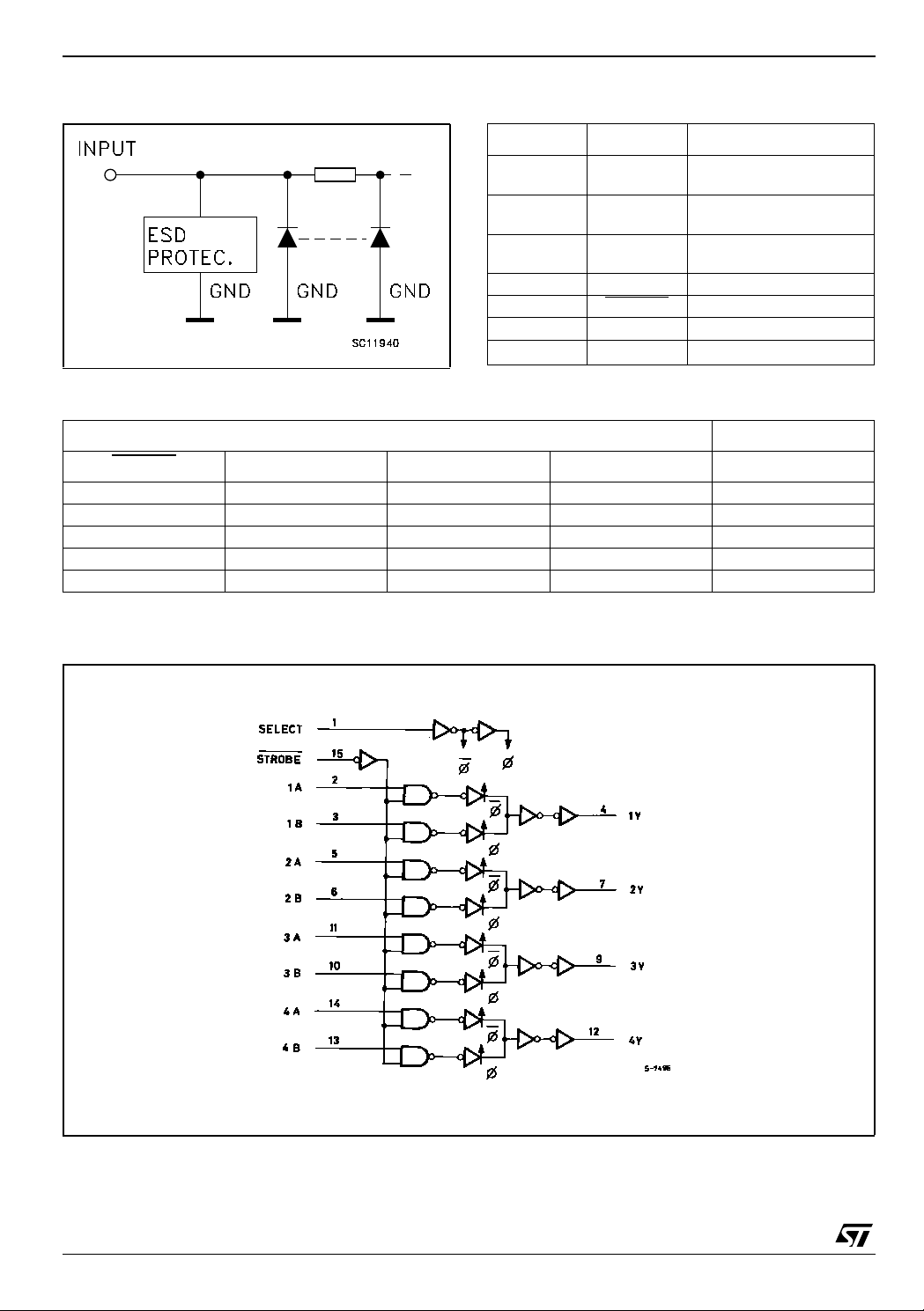
Figure 2: Input Equivalent Circuit Table 2: Pin Description
PIN N° SYMBOL NAME AND FUNCTION
1 SELECT Common Data Select
Inputs
2, 5, 11, 14 1A to 4A Data Inputs From Source
A
3, 6, 10, 13 1B to 4B Data Inputs From Source
B
4, 7, 9, 12 1Y to 4Y Multiplexer Outputs
15 STROBE Strobe Input
8 GND Ground (0V)
Positive Supply Voltage
Table 3: Truth Table
16 V
INPUTS OUTPUT
CC
STROBE
HXXXL
LLLXL
LLHXH
LHXLL
LHXHH
X : Don’t ca re
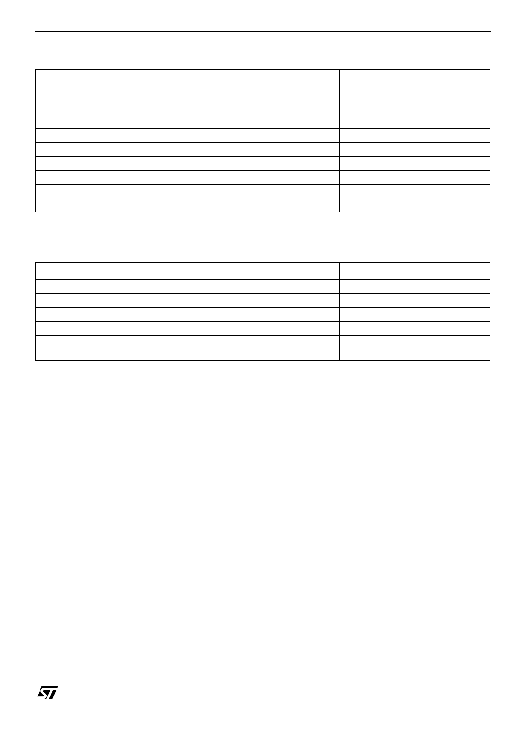
Figure 3: Logic Diagram
SELECT A B Y
2/12
74VHC157
Table 4: Absolute Maximum Ratings
Symbol Parameter Value Unit
V
V
V
I
I
OK
I
or I
I
CC
T
T
Absolute Maximum Ratings are those values beyond which damage to the device may occur. Functional operation under these conditions is
not implied
Table 5: Recommended Operating Conditions
Symbol Parameter Value Unit
V
V
V
T
dt/dv
Supply Voltage
CC
DC Input Voltage
I
DC Output Voltage -0.5 to VCC + 0.5
O
DC Input Diode Current
IK
DC Output Diode Current
DC Output Current
O
DC VCC or Ground Current
GND
Storage Temperature
stg
Lead Temperature (10 sec)
L
Supply Voltage
CC
Input Voltage
I
Output Voltage 0 to V
O
Operating Temperature
op
Input Rise and Fall Time (note 1) (V
(V
= 3.3 ± 0.3V)
CC
= 5.0 ± 0.5V)
CC
-0.5 to +7.0 V
-0.5 to +7.0 V
- 20 mA
± 20 mA
± 25 mA
± 50 mA
-65 to +150 °C
300 °C
2 to 5.5 V
0 to 5.5 V
CC
-55 to 125 °C
0 to 100
0 to 20
ns/V
V
V
1) VIN from 30 % t o 70% of V
CC
3/12
74VHC157
Table 6: DC Specifications
Symbol Parameter
V
V
V
High Level Input
IH
Voltage
V
Low Level Input
IL
Voltage
High Level Output
OH
Voltage
Low Level Output
OL
Voltage
Input Leakage
I
I
Current
Quiescent Supply
I
CC
Current
V
3.0 to
3.0 to
0 to
Test Condition Value
= 25°C
(V)
CC
T
A
Min. Typ. Max. Min. Max. Min. Max.
-40 to 85°C -55 to 125°C
2.0 1.5 1.5 1.5
5.5
0.7V
CC
0.7V
CC
0.7V
CC
2.0 0.5 0.5 0.5
5.5
2.0
3.0
4.5
3.0
4.5
2.0
3.0
4.5
3.0
4.5
5.5
5.5
=-50 µA
I
O
=-50 µA
I
O
=-50 µA
I
O
I
=-4 mA
O
=-8 mA
I
O
=50 µA
I
O
=50 µA
I
O
I
=50 µA
O
=4 mA
I
O
=8 mA
I
O
V
= 5.5V or GND
I
= VCC or GND
V
I
0.3V
CC
1.9 2.0 1.9 1.9
2.9 3.0 2.9 2.9
4.4 4.5 4.4 4.4
2.58 2.48 2.4
3.94 3.8 3.7
0.0 0.1 0.1 0.1
0.0 0.1 0.1 0.1
0.0 0.1 0.1 0.1
0.36 0.44 0.55
0.36 0.44 0.55
± 0.1 ± 1 ± 1 µA
44040µA
0.3V
CC
0.3V
CC
Unit
V
V
V
V
Table 7: AC Electrical Characteristics (Input t
Test Condition Value
Symbol Parameter
t
Propagation Delay
PLH
t
t
t
t
t
(*) Voltage range is 3.3V ± 0.3V
(**) Voltage range is 5.0V ±
Time
PHL
A, B to Y
Propagation Delay
PLH
Time
PHL
SELECT to Y
Propagation Delay
PLH
Time STROBE
PHL
0.5V
to Y
V
3.3
3.3
5.0
5.0
3.3
3.3
5.0
5.0
3.3
3.3
5.0
5.0
C
CC
(V)
L
(pF)
(*)
15 6.2 9.7 1.0 11.5 1.0 11.5
(*)
50 8.7 13.2 1.0 15.0 1.0 15.0
(**)
15 4.1 6.4 1.0 7.5 1.0 7.5
(**)
50 5.6 8.4 1.0 9.5 1.0 9.5
(*)
15 8.4 13.2 1.0 15.5 1.0 15.5
(*)
50 10.9 16.7 1.0 19.0 1.0 19.0
(**)
15 5.3 8.1 1.0 9.5 1.0 9.5
(**)
50 6.8 10.1 1.0 11.5 1.0 11.5
(*)
15 8.7 13.6 1.0 16.0 1.0 16.0
(*)
50 11.2 17.1 1.0 19.5 1.0 19.5
(**)
15 5.6 8.6 1.0 10.0 1.0 10.0
(**)
50 7.1 10.6 1.0 12.0 1.0 12.0
= tf = 3ns)
r
= 25°C
T
A
-40 to 85°C -55 to 125°C
Min. Typ. Max. Min. Max. Min. Max.
Unit
ns
ns
ns
4/12
 Loading...