

74VHC138
3 TO 8 LINE DECODER (INVERTING)
■ HIGH SPEED: t
■ LOW POWER DISSIPATION:
I
= 4 µA (MAX.) at TA=25°C
CC
■ HIGH NOISE IMMUNITY:
V
= V
NIH
■ POWER DOWN PROTECTION ON INPUTS
■ SYMMETRICAL OUTPUT IMPEDANCE:
|I
OH
■ BALANCED PROPAGATION DELAYS:
t
PLH
■ OPERATING VOLTAGE RANGE:
V
CC
■ PIN AND FUNCTION COMPATIBLE WITH
NIL
| = IOL = 8 mA (MIN)
≅ t
PHL
(OPR) = 2V to 5.5V
= 5.7ns (TYP.) at VCC = 5V
PD
= 28% VCC (MIN.)
74 SERIES 138
■ IMPROVED LATCH-UP IMMUN ITY
DESCRIPTION
The 74VHC138 is an advanced high-speed
CMOS 3 TO 8 LINE DECODER (INVERTING)
fabricated with sub-micron silicon gate and
double-layer metal wiring C
2
MOS technology.
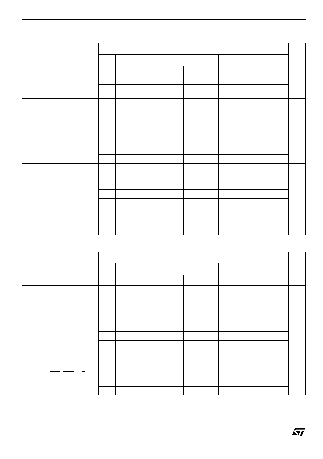
If the device is enabled, 3 binary select (A, B, and
C) determine which one of the outputs will go low.
If enable input G1 is held low or either G2A
or G2B
is held high, the decoding function is inhibited and
all the 8 outputs go to high.
TSSOPSOP
Table 1: Order Codes
PACKAGE T & R
SOP 74VHC138MTR
TSSOP 74VHC138TTR
Tree enable inpu ts are provided to ease cascade
connection and application of address decoders
for memory systems.
Power down protection is provided on all inputs
and 0 to 7V can be accepted on inputs with no
regard to the supply voltage. This device can be
used to interface 5V to 3V.
All inputs and outputs are equipped with
protection circuits against static disc harge, giving
them 2KV ESD immunity and transient excess
voltage.
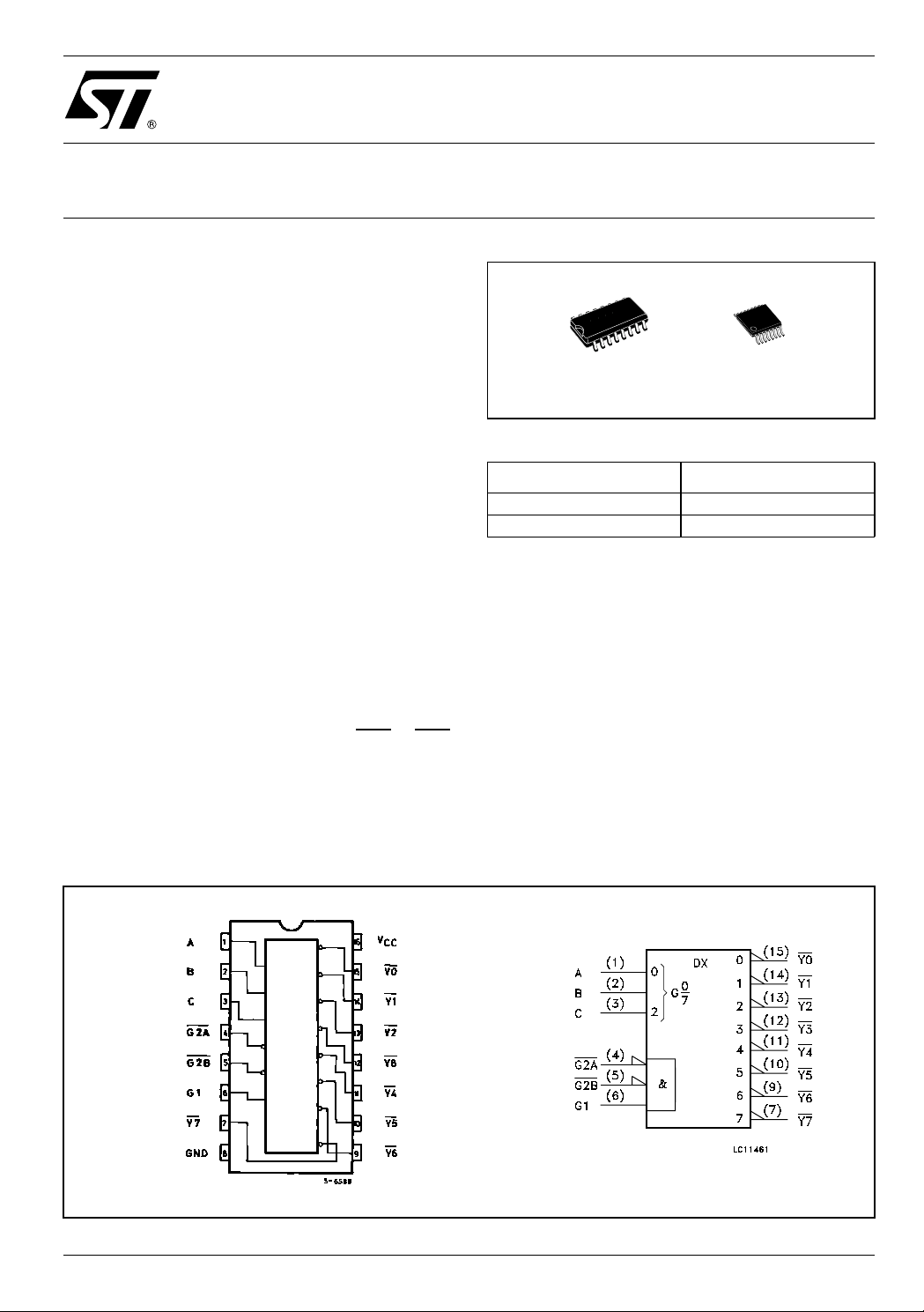
Figure 1: Pin Connection An d I E C Logic Symbols
Rev. 4
1/12November 2004
74VHC138
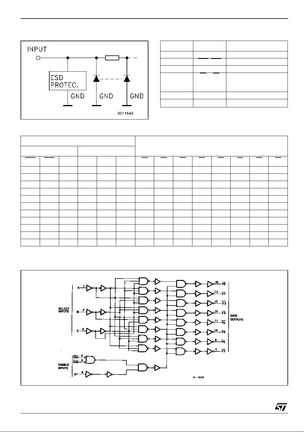
Figure 2: Input Equivalent Circuit Table 2: Pin Description
PIN N° SYMBOL NAME AND FUNCTION
1, 2, 3 A, B, C Address Inputs
4, 5 G2A
6 G1 Enable Input
15, 14, 13,
12, 1 1, 10, 9,
7
8 GND Ground (0V)
16 V
Table 3: Truth Table
, G2B Enable Inputs
to Y7 Outputs
Y0
CC
Positive Supply Voltage
INPUTS
ENABLE SELECT
G2B
X : Don’t care
G2A G1CBAY0Y1 Y2 Y3 Y4 Y5 Y6 Y7
XXLXXXHHHHHHHH
XHXXXXHHHHHHHH
HXXXXXHHHHHHHH
LLHLLLLHHHHHHH
LLHLLHHLHHHHHH
LLHLHLHHLHHHHH
LLHLHHHHHLHHHH
LLHHLLHHHHLHHH
LLHHLHHHHHHLHH
LLHHHLHHHHHHLH
LLHHHHHHHHHHHL
OUTPUTS
Figure 3: Logic Diagram
This logi c di agram has not be used to est i m ate propaga tion delays
2/12
74VHC138
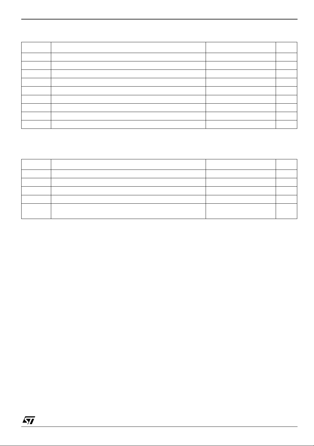
Table 4: Absolute Maximum Ratings
Symbol Parameter Value Unit
V
V
V
I
I
OK
I
or I
I
CC
T
T
Absolute Maximum Ratings are those values beyond which damage to the device may occur. Functional operation under these conditions is
not implied
Table 5: Recommended Operating Conditions
Symbol Parameter Value Unit
V
V
V
T
dt/dv
Supply Voltage
CC
DC Input Voltage
I
DC Output Voltage -0.5 to VCC + 0.5
O
DC Input Diode Current
IK
DC Output Diode Current
DC Output Current
O
DC VCC or Ground Current
GND
Storage Temperature
stg
Lead Temperature (10 sec)
L
Supply Voltage
CC
Input Voltage
I
Output Voltage 0 to V
O
Operating Temperature
op
Input Rise and Fall Time (note 1) (V
(V
= 3.3 ± 0.3V)
CC
= 5.0 ± 0.5V)
CC
-0.5 to +7.0 V
-0.5 to +7.0 V
- 20 mA
± 20 mA
± 25 mA
± 75 mA
-65 to +150 °C
300 °C
2 to 5.5 V
0 to 5.5 V
CC
-55 to 125 °C
0 to 100
0 to 20
ns/V
V
V
1) VIN from 30 % t o 70% of V
CC
3/12
74VHC138
Table 6: DC Specifications
Symbol Parameter
V
V
V
High Level Input
IH
Voltage
V
Low Level Input
IL
Voltage
High Level Output
OH
Voltage
Low Level Output
OL
Voltage
I
Input Leakage
I
Current
I
Quiescent Supply
CC
Current
3.0 to
3.0 to
Test Condition Value
V
(V)
CC
T
A
Min. Typ. Max. Min. Max. Min. Max.
-40 to 85°C -55 to 125°C
= 25°C
2.0 1.5 1.5 1.5
5.5
0.7V
CC
0.7V
CC
0.7V
CC
2.0 0.5 0.5 0.5
5.5
2.0
3.0
4.5
3.0
4.5
2.0
3.0
4.5
3.0
4.5
0 to
VI = 5.5V or GND
5.5
V
5.5
IO=-50 µA
I
=-50 µA
O
=-50 µA
I
O
=-4 mA
I
O
=-8 mA
I
O
IO=50 µA
=50 µA
I
O
=50 µA
I
O
=4 mA
I
O
=8 mA
I
O
= VCC or GND
I
0.3V
CC
1.9 2.0 1.9 1.9
2.9 3.0 2.9 2.9
4.4 4.5 4.4 4.4
2.58 2.48 2.4
3.94 3.8 3.7
0.0 0.1 0.1 0.1
0.0 0.1 0.1 0.1
0.0 0.1 0.1 0.1
0.36 0.44 0.55
0.36 0.44 0.55
± 0.1 ± 1 ± 1 µA
44040µA
0.3V
CC
0.3V
CC
Unit
V
V
V
V
Table 7: AC Electrical Characteristics (Input t
Test Condition Value
Symbol Parameter
t
Propagation Delay
PLH
t
t
t
t
t
(*) Voltage range is 3.3V ± 0.3V
(**) Voltage range is 5.0V ±
Time
PHL
A, B, C, to Y
Propagation Delay
PLH
Time
PHL
G to Y
Propagation Delay
PLH
Time
PHL
G2A
, G2B to Y
0.5V
V
3.3
3.3
5.0
5.0
3.3
3.3
5.0
5.0
3.3
3.3
5.0
5.0
C
CC
(V)
L
(pF)
(*)
15 8.2 11.4 1.0 13.0 1.0 13.0
(*)
50 10.0 15.8 1.0 18.0 1.0 18.0
(**)
15 5.7 8.1 1.0 9.5 1.0 9.5
(**)
50 7.2 10.1 1.0 11.5 1.0 11.5
(*)
15 8.1 12.8 1.0 15.0 1.0 15.0
(*)
50 10.6 16.3 1.0 18.5 1.0 18.5
(**)
15 5.6 8.1 1.0 9.5 1.0 9.5
(**)
50 7.1 10.1 1.0 11.5 1.0 11.5
(*)
15 8.2 11.4 1.0 13.5 1.0 13.5
(*)
50 10.7 14.9 1.0 17.0 1.0 17.0
(**)
15 5.8 8.1 1.0 9.5 1.0 9.5
(**)
50 7.3 10.1 1.0 11.5 1.0 11.5
= tf = 3ns)
r
= 25°C
T
A
-40 to 85°C -55 to 125°C
Min. Typ. Max. Min. Max. Min. Max.
Unit
ns
ns
ns
4/12
 Loading...