

ST 74VHC05 User Manual
74VHC05
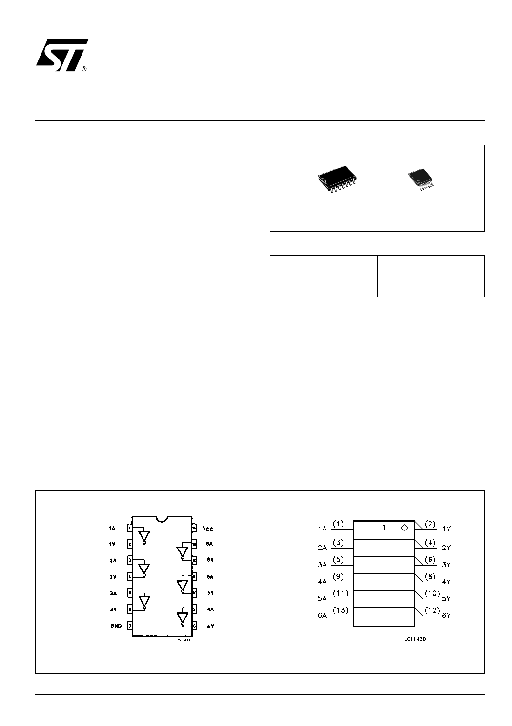
HEX INVERTER (OPEN DRAIN)
■ HIGH SPEED: t
■ LOW POWER DISSIPATION:
I
= 2 µA (MAX.) at TA=25°C
CC
■ HIGH NOISE IMMUNITY:
V
= V
NIH
■ POWER DOWN PROTECTION ON INPUTS
■ OPERATING VOLTAGE RANGE:
V
CC
■ PIN AND FUNCTION COMPATIBLE WITH
NIL
(OPR) = 2V to 5.5V
= 3.8ns (TYP.) at VCC = 5V
PD
= 28% VCC (MIN.)
74 SERIES 05
■ IMPROVED LATCH-UP IMMUN ITY
■ LOW NOISE: V
= 0.8V (MAX.)
OLP
DESCRIPTION
The 74VHC05 is an advanced high-speed CMOS
OPEN DRAIN HEX INVERTER fabricated with
sub-micron silicon gate and double-layer metal
wiring C
2
MOS technology.
The internal circuit is composed of 3 stages
including buffer ou tput, whi ch provid es hig h no ise
immunity and stable output.
Power down protection is provided on all inputs
and 0 to 7V can be accepted on inputs with no
TSSOPSOP
Table 1: Order Codes
PACKAGE T & R
SOP 74VHC05MTR
TSSOP 74VHC05TTR
regard to the supply voltage. This device can be
used to interface 5V to 3V.
All inputs and outputs are equipped with
protection circuits against static disc harge, giving
them 2KV ESD immunity and transient excess
voltage.
Figure 1: Pin Connection An d I E C Logic Symbols
Rev. 5
1/11November 2004
74VHC05
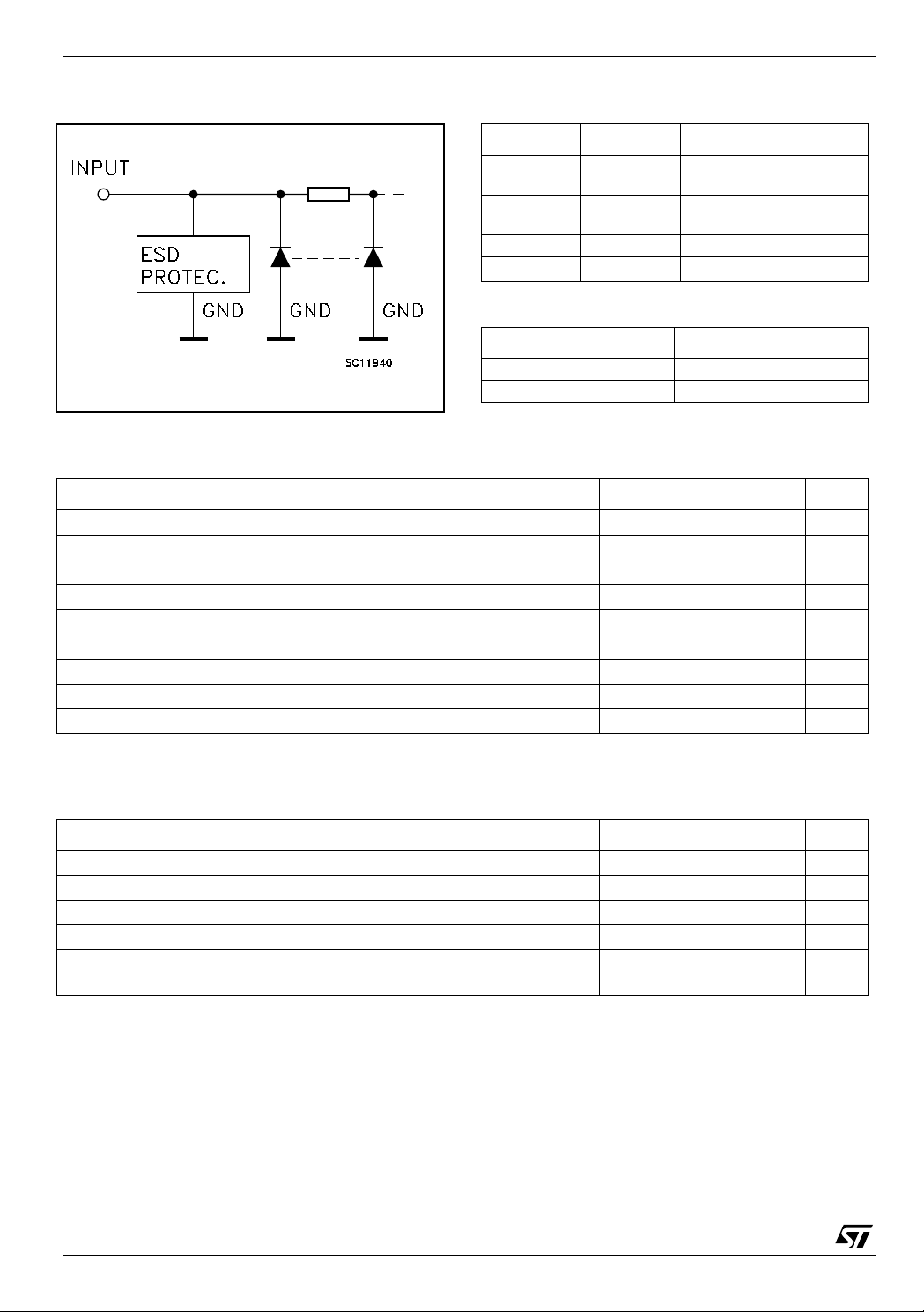
Figure 2: Inp ut Eq ui v al e nt C irc ui t Table 2: Pin Des cription
PIN N° SYMBOL NAME AND FUNCTION
1, 3, 5, 9, 1 1,
13
2, 4, 6, 8, 10,
12
7 GND Ground (0V)
14
Table 3: Trut h Table
Z: High Imped ance
Table 4: Absolute Maximum Ratings
Symbol Parameter Value Unit
V
V
V
I
I
OK
I
or I
I
CC
T
T
Absolute Maximum Ratings are those values beyond which damage to the device may occur. Functional operation under these conditions is
not implied
Supply Voltage
CC
DC Input Voltage
I
DC Output Voltage -0.5 to VCC + 0.5
O
DC Input Diode Current
IK
DC Output Diode Current
DC Output Current
O
DC VCC or Ground Current
GND
Storage Temperature
stg
Lead Temperature (10 sec)
L
Table 5: Recommended Operating Conditions
1A to 6A Data Inputs
1Y to 6Y Data Outputs
V
CC
Positive Supply Voltage
AY
LZ
HL
-0.5 to +7.0 V
-0.5 to +7.0 V
V
- 20 mA
± 20 mA
± 25 mA
± 75 mA
-65 to +150 °C
300 °C
Symbol Parameter Value Unit
V
V
V
T
dt/dv
1) VIN from 30% to 70% of V
Supply Voltage
CC
Input Voltage
I
Output Voltage 0 to V
O
Operating Temperature
op
Input Rise and Fall Time (note 1) (V
(V
CC
= 3.3 ± 0.3V)
CC
= 5.0 ± 0.5V)
CC
2 to 5.5 V
0 to 5.5 V
CC
-55 to 125 °C
0 to 100
0 to 20
2/11
V
ns/V
Table 6: DC Specifications
Symbol Parameter
V
V
High Level Input
IH
Voltage
V
Low Level Input
IL
Voltage
Low Level Output
OL
Voltage
I
High Impedance
OZ
Output Leakage
Current
Input Leakage
I
I
Current
Quiescent Supply
I
CC
Current
V
(V)
2.0 1.5 1.5 1.5
3.0 to
5.5
2.0 0.5 0.5 0.5
3.0 to
5.5
2.0
3.0
4.5
3.0
4.5
5.5
0 to
5.5
5.5
Test Condition Value
= 25°C
T
CC
A
Min. Typ. Max. Min. Max. Min. Max.
0.7V
CC
0.3V
CC
IO=50 µA
I
=50 µA
O
=50 µA
I
O
=4 mA
I
O
=8 mA
I
O
= VIH or V
V
I
IL
VO = VCC or GND
= 5.5V or GND
V
I
= VCC or GND
V
I
0.0 0.1 0.1 0.1
0.0 0.1 0.1 0.1
0.0 0.1 0.1 0.1
0.36 0.44 0.55
0.36 0.44 0.55
±0.25 ± 2.5 ± 2.5 µA
± 0.1 ± 1 ± 1 µA
22020µA
74VHC05
-40 to 85°C -55 to 125°C
0.7V
CC
0.3V
CC
0.7V
CC
0.3V
CC
Unit
V
V
V
Table 7: AC Electrical Characteristics (Input t
Test Condition Value
Symbol Parameter
t
t
(*) Voltage range is 3.3V ± 0.3V
(**) Voltage range is 5.0V ±
PZL
PLZ
Output Enable
Time
Output Disable
Time
0.5V
V
3.3
3.3
5.0
5.0
3.3
5.0
(V)
CC
(*)
(*)
(**)
(**)
(*)
(**)
C
(pF)
15
50
15
50
50
50
L
R
= 1 KΩ
L
R
= 1 KΩ
L
R
= 1 KΩ
L
R
= 1 KΩ
L
R
= 1 KΩ
L
R
= 1 KΩ
L
= tf = 3ns)
r
= 25°C
T
A
-40 to 85°C -55 to 125°C
Min. Typ. Max. Min. Max. Min. Max.
5.0 7.1 1.0 8.5 1.0 8.5
7.5 10.6 1.0 12.0 1.0 12.0
3.8 5.5 1.0 6.5 1.0 6.5
5.3 7.5 1.0 8.5 1.0 8.5
7.5 10.6 1.0 12.0 1.0 12.0
5.3 7.5 1.0 8.5 1.0 8.5
Unit
ns
ns
3/11
74VHC05
Table 8: Capacitive Characteristics
Test Condition Value
= 25°C
Symbol Parameter
T
A
Min. Typ. Max. Min. Max. Min. Max.
C
C
C
Input Capacitance
IN
Output
OUT
Capacitance
Power Dissipation
PD
Capacitance
610 10 10pF
8pF
3pF
(note 1)
1) CPD is defined as the value of the IC’s internal equivalent capacitance which is calculated from the operating current consumption without
load. (Refer to Test Circuit). Average operating current can be obtained by the following equation. I
Table 9: Dynamic Switching Characteristics
Test Condition Value
= 25°C
Symbol Parameter
V
V
Dynamic Low
OLP
Voltage Quiet
OLV
Output (note 1, 2)
Dynamic High
V
IHD
Voltage Input
(note 1, 3)
Dynamic Low
V
ILD
Voltage Input
(note 1, 3)
V
CC
(V)
5.0
= 50 pF
5.0 3.5 V
C
L
5.0 1.5 V
T
A
Min. Typ. Max. Min. Max. Min. Max.
0.4 0.8
-0.8 -0.4
-40 to 85°C -55 to 125°C
= CPD x VCC x fIN + ICC/6 (per gate)
CC(opr)
-40 to 85°C -55 to 125°C
Unit
Unit
V
1) Worst case package.
2) Max number of outp ut s defined as (n). Data inpu t s are driven 0V to 5.0V, (n-1) outputs switc hi ng and one output at GND.
3) Max number of data inputs (n) switching. (n-1) switching 0V to 5.0V. Inputs under test switching: 5.0V to threshold (V
(V
), f=1MHz.
IHD
ILD
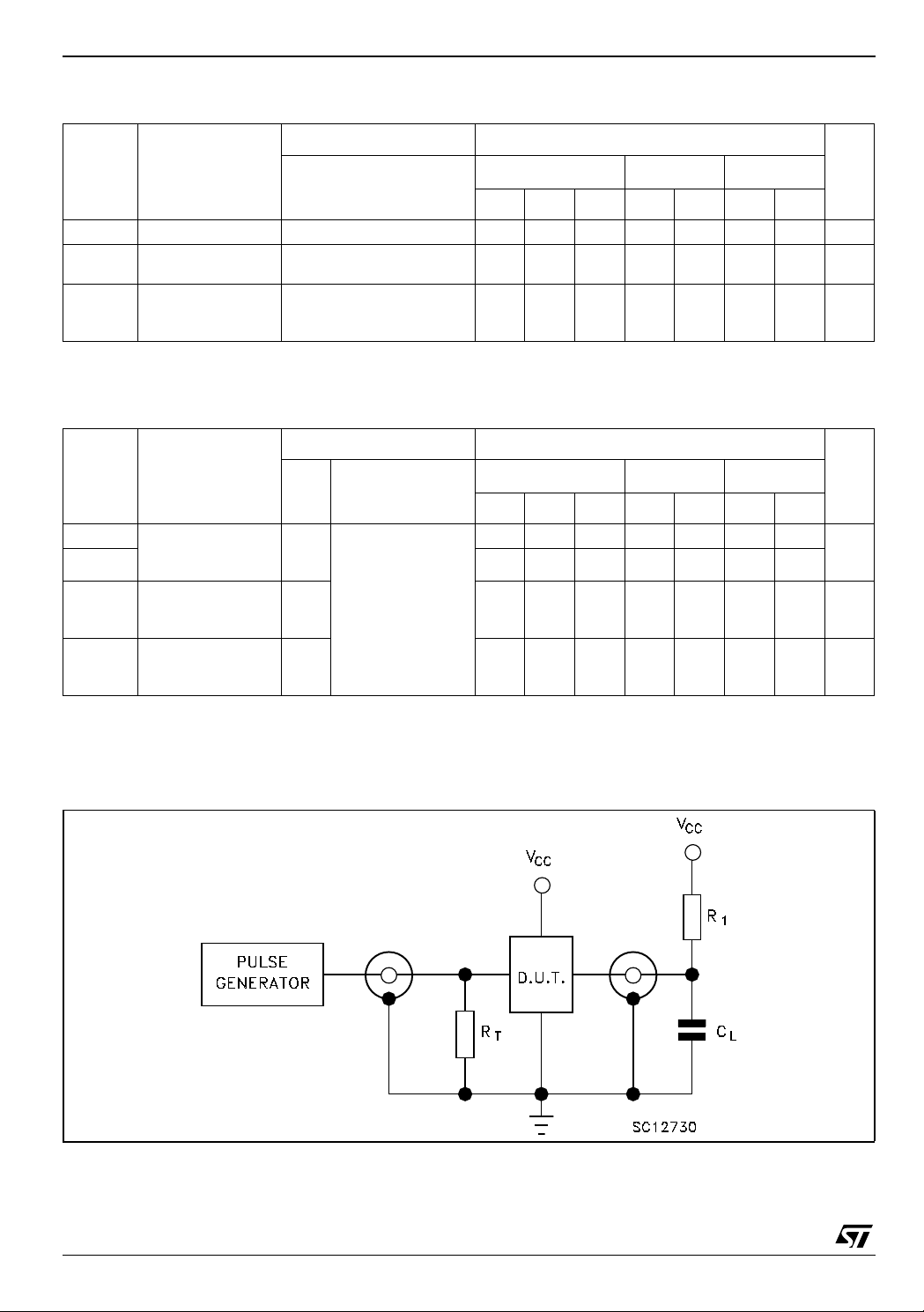
Figure 3: Test Circuit
CL = 15/50pF or e qui valent (inc lu des jig and pro be capacitan ce)
= R1 = 1KΩ or equivalent
R
L
R
= Z
of pulse generator (typically 50Ω)
T
OUT
), 0V to thresho l d
4/11
 Loading...