

查询74V2T66供应商
■ HIGH SPEED:
t
= 0.6ns (TYP.) at VCC=5V
PD
■ COMPATIBLE WITH TTL LEVEL
■ LOW POWER DISSIPATION:
I
=1µA(MAX.) at TA= 25°C
CC
■ LOW "ON" RESISTANCE:
R
=10Ω (TYP.) AT VCC=5VI
ON
■ SINE WAV E DIS TORTION:
0.04% AT V
■ OPERATING VOLTAGERANGE:
V
(OPR) = 4.5V TO 5.5V
CC
■ IMPROVED LATCH-UP IMMUNITY
=5.0V,f=1KHz
CC
I/O
=1mA
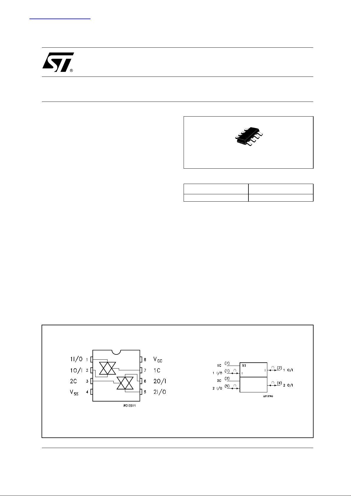
74V2T66
DUAL BILATERAL SWITCH
SOT23-8L
ORDER CODES
PACKAGE T & R
SOT23-8L 74V2T66STR
DESCRIPTION
The 74V2T66 is an advanced high-speed CMOS
DUAL BILATERAL SWITCH fabricated in silicon
gate C
2
MOS technology. It achieves high speed
propagation delay and VERY LOW ON
resistances while maintaining true CMOS low
power consumption. This b ilateral switch handles
rail to rail analog and digital signals that may vary
across the full power supply range (from GND to
V
)
CC
The C input is provided to control the switch and
it’s compatible with standard CMOS output; the
PIN CONNECTION AND IEC LOGIC SYMBOLS
switch is ON (port I/O is connected to Port O/ I)
when the C input is held high and OFF (high
impedance state exists between the t w o ports)
when C is held low. It can be used in many
application as Battery P owered System, T est
Equipment. It’s available in the comm erc ial and
extended temperature range in SOT23-8L
package. All inputs and output are equipped with
protection circuits against static discharge, gi v ing
them ESD immunity and tra nsient excess voltage.
1/9June 2003
74V2T66
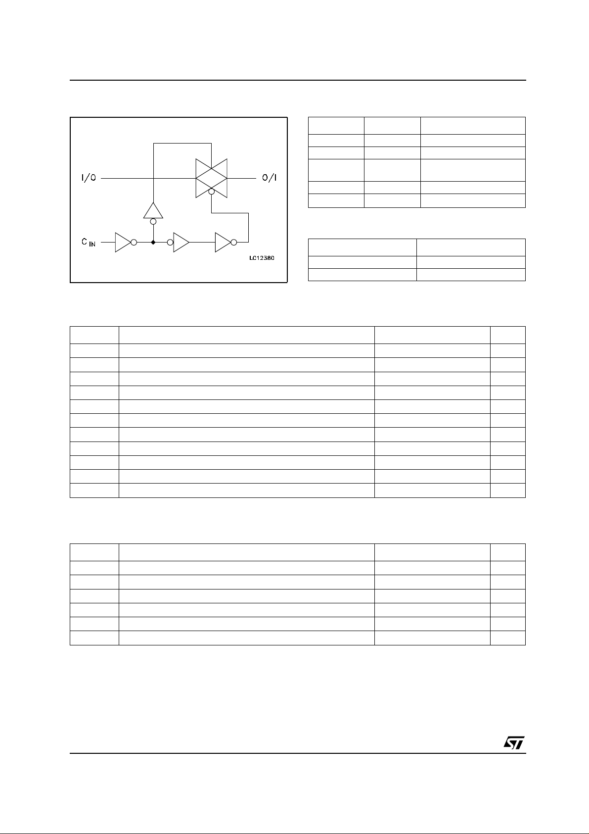
INPUT EQUIVALENT CIRCUIT PIN DESCRIPTION
PIN No SYMBOL NAME AND FUNCTION
1, 5 1I/O, 2I/O Independent Input/Output
2, 6 1O/I, 2O/I Independent Output/Input
7, 3 1C, 2C
4 GND Ground (0V)
8
V
CC
TRUTH TABLE
CONTROL SWITCH FUNCTION
HON
L OFF *
* : High Impedance State
ABSOLUTE MAXIMUM RATINGS
Symbol Parameter Value Unit
V
V
V
V
I
I
I
OK
I
or I
I
CC
T
T
Absolute Maximum Ratings are those values beyond which damage to the device may occur. Functional operation under these conditions is
not implied
Supply Voltage
CC
DC Input Voltage -0.5 to VCC+ 0.5
I
DC Control Input Voltage
IC
DC Output Voltage -0.5 to VCC+ 0.5
O
DC Input Diode Current
IK
DC Control Input Diode Current
IK
DC Output Diode Current
DC Output Current
O
DC VCCor Ground Current
GND
Storage Temperature
stg
Lead Temperature (10 sec)
L
Enable Input (Active
HIGH)
Positive Supply Voltage
-0.5 to +7.0 V
V
-0.5 to +7.0 V
V
± 20 mA
-20 mA
± 20 mA
± 50 mA
± 50 mA
-65 to +150 °C
300 °C
RECOMMENDED OPERATING CONDITIONS
Symbol Parameter Value Unit
V
V
V
V
T
dt/dv
1) VINfrom0.8V to 2V on control pin
2/9
Supply Voltage
CC
Input Voltage 0 to V
I
Control Input Voltage
IC
Output Voltage 0 to V
O
Operating Temperature
op
Input Rise and Fall Time (note 1) V
CC
= 5.0V
4.5 to 5.5 V
CC
0 to 5.5 V
CC
-55 to 125 °C
0 to 20 ns/V
V
V
DC SPECIFICATIONS
Symbol Parameter
V
R
R
I
I
(*) Voltage range is5V± 0.5V
High Level Input
IH
Voltage
V
Low Level Input
IL
Voltage
ON Resistance
ON
ON Resistance
ON
Input/Output
OFF
Leakage Current
(SWITCH OFF)
I
Switch Input
IZ
Leakage Current
(SWITCH ON,
OUTPUT OPEN)
Control Input
I
IN
Leakage Current
Quiescent Supply
CC
Current
Test Condition Value
= 25°C
T
V
(V)
5.0
5.0
5.0
5.0
CC
(*)
(*)
(*)
(*)
VIC=V
V
I/O=VCC
I
I/O
VIC=V
V
I/O=VCC
I
I/O
IH
to GND
≤ 1mA
IH
or GND
≤ 1mA
A
Min. Typ. Max. Min. Max. Min. Max.
222V
12 17 20 24 V
10 14 18 20 V
5.5 VOS=VCCto GND
V
IS=VCC
V
IC=VIL
to GND
5.5
to GND
V
IC=VIH
= 5.5V or GND
or GND
± 0.1 ± 1.0 ± 1.0 µA
0to
5.5
5.5
V
OS=VCC
V
IC
V
I=VCC
74V2T66
-40 to 85°C -55 to 125°C
0.8 0.8 0.8 V
±0.1 ± 1 ± 1 µA
±0.1 ± 1 ± 5 µA
11020µA
Unit
AC ELECTRICAL CHARACTERISTICS (CL= 50pF, Input tr=tf= 3ns)
Test Condition Value
= 25°C
Symbol Parameter
t
t
PLZ
t
PHZ
t
PZL
t
PZH
(*) Voltage range is5.0V ± 0.5V
PD
Delay Time
Output Disable
Time
Output Enable
Time
V
(V)
5.0
5.0
5.0
CC
(*)
(*)
(*)
RL= 500 Ω
RL=1KΩ
T
A
Min. Typ. Max. Min. Max. Min. Max.
0.6 0.7 1.0 2.0 ns
6.0 7.5 9.0 10.0 ns
2.5 4.0 5.0 7.0 ns
-40 to 85°C -55 to 125°C
Unit
3/9

74V2T66
CAPACITIVE CHARACTERISTICS
Test Condition Value
= 25°C
Symbol Parameter
T
A
Min. Typ. Max. Min. Max. Min. Max.
C
C
C
Input Capacitance
IN
Output
I/O
Capacitance
Power Dissipation
PD
Capacitance
410 10 10pF
10 pF
3pF
(note 1)
1) CPDis defined as the value of the IC’s internal equivalent capacitance which is calculated from the operating current consumption without
load. (Refer to Test Circuit). Average operating current can be obtained by the following equation. I
ANALOG SWITCH CHARACTERISTICS (GND = 0V; TA= 25°C)
Test Condition Value
Symbol Parameter
Sine Wave
Distortion (THD)
MAX
Frequency
Response
f
(Switch ON)
Feedthrough
Attenuation
(Switch OFF)
Crosstalk (Control
Input to Signal
Output)
CrosstalkBetween
Switches
(*) Voltage range is 5.0V ± 0.5V
5.0(*) 4
5.0(*) Adjust fINvoltage to obtain 0 dBm at VOS.
5.0(*) V
5.0(*) R
5.0(*) R
V
(V)
CC
(V
V
p-p
IN
)
=1KHzRL=10KΩ,CL=50pF
f
IN
Increase f
Adjust f
Frequency until dB meter reads -3dB
IN
=50Ω,CL=10pF
R
L
is centered at VCC/2
IN
Voltage to obtained 0dBm at V
IN
RL= 600Ω,CL=50pF,fIN= 1MHz sine wave
= 600Ω,CL=50pF,fIN= 1MHz square wave
L
tr=tf= 2.0ns
= 600Ω,CL=50pF,fIN= 1MHz sine wave -60 dB
L
-40 to 85°C -55 to 125°C
CC(opr)=CPDxVCCxfIN+ICC
Typ.
0.04 %
180 MHz
IS
Unit
/2(per switch)
Unit
-60 dB
60 mV
4/9

SWITCHINGCARACTERISTICSTESTCIRCUIT
74V2T66
FEEDTHROUGH ATTENUATION
BANDWIDTH ATTENUATION
MAXIMUM CONTROL FREQUENCY
CROSSTALK (control to output
5/9

74V2T66
CHANNEL RESISTANCE (R
ON)
ICC(Opr.)
6/9

74V2T66
SOT23-8L MECHANICAL DATA
mm. mils
DIM.
MIN. TYP MAX. MIN. TYP. MAX.
A 0.90 1.45 35.4 57.1
A1 0.00 0.15 0.0 5.9
A2 0.90 1.30 35.4 51.2
b 0.22 0.38 8.6 14.9
C 0.09 0.20 3.5 7.8
D 2.80 3.00 110.2 118.1
E 2.60 3.00 102.3 118.1
E1 1.50 1.75 59.0 68.8
e0.65 25.6
e1 1.95 76.7
L 0.35 0.55 13.7 21.6
7/9

74V2T66
Tape & Reel SOT23-xL MECHANICAL DATA
DIM.
MIN. TYP MAX. MIN. TYP. MAX.
A 180 7.086
C 12.8 13.0 13.2 0.504 0.512 0.519
D 20.2 0.795
N 60 2.362
T 14.4 0.567
Ao 3.13 3.23 3.33 0.123 0.127 0.131
Bo 3.07 3.17 3.27 0.120 0.124 0.128
Ko 1.27 1.37 1.47 0.050 0.054 0.0.58
Po 3.9 4.0 4.1 0.153 0.157 0.161
P 3.9 4.0 4.1 0.153 0.157 0.161
mm. inch
8/9

74V2T66
Information furnished is believed to be accurate and reliable. However, STMicroelectronics assumes no responsibility for the
consequences of use of such informatio n nor for any infringement of paten ts or o ther rig hts of t hird part ies which ma y result from
its use. No license is granted by implication or otherwise under any patent or patent rights of STMicroelectronics. Specifications
mentioned in this publication are subject to change without notice. This publication supersedes and replaces all information
previousl y suppl ied. STM icroel ectronics produc ts are not auth orized for use as c ritica l compone nts in l ife s upport dev ices or
systems without express written approval of STMicroelectronics.
Australia - Brazil - Canada - China - Finland - France - Germany - Hong Kong - India - Israel - Italy - Japan - Malaysia - Malta - Morocco
© The ST logo is a registered trademark of STMicroelectronics
© 2002 STMicroelectronics - Printed in Italy - All Rights Reserved
STMicroelectronics GROUP OF COMPANIES
Singapore - Spain - Sweden - Switzerland - United Kingdom - United States.
© http://www.st.com
9/9

WWW.ALLDATASHEET.COM
Copyright © Each Manufacturing Company.
All Datasheets cannot be modified without permission.
This datasheet has been download from :
www.AllDataSheet.com
100% Free DataSheet Search Site.
Free Download.
No Register.
Fast Search System.
www.AllDataSheet.com
 Loading...