

查询74V2T14供应商
74V2T14
TRIPLE S CHMITT INVERTER
■ HIGH SPEED: t
■ LOW POWER DISSIPATION:
I
=1µA(MAX.) atTA=25°C
CC
■ TYPICAL HYSTERESIS:
V
=700mV at VCC=4.5V
h
■ POWER DOWN PROTECTION ON INPUT
■ SYMMETRICAL OUTPUT IMPEDANCE:
|I
|=IOL=8mA(MIN)atVCC=4.5V
OH
■ BALANCED PROPAGATION DELAYS:
t
≅ t
PLH
PHL
■ OPERATING VOLTAGE RANG E:
V
(OPR) = 4.5V to 5.5V
CC
■ IMPROVED LATCH-UP IMMUNITY
= 5.0ns (TYP.) at VCC=5V
PD
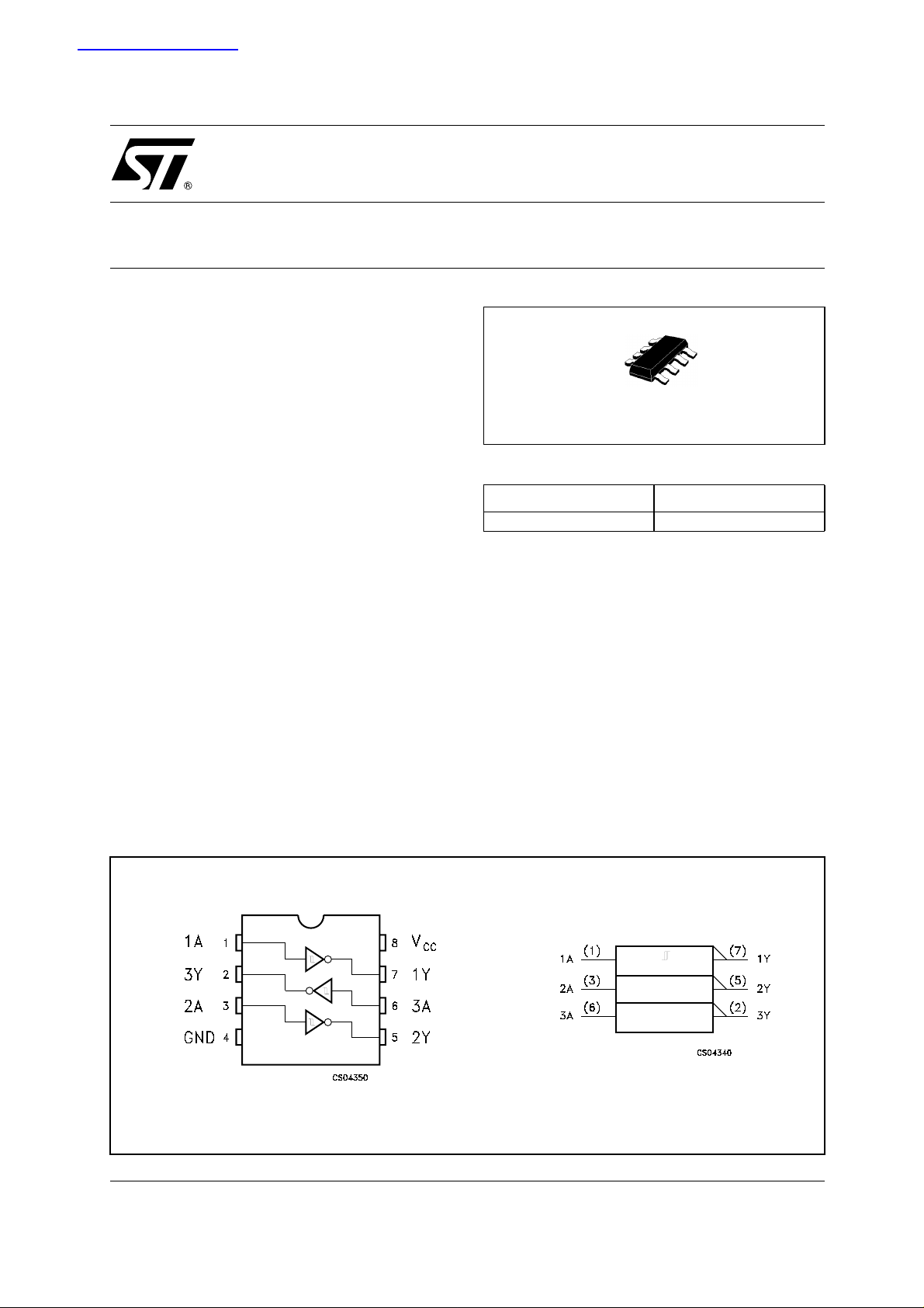
DESCRIPTION
The 74V2T14 is an advanced high-speed CMOS
TRIPLE SCHMITT INVERTER fabricated with
sub-micron silicon gate and double-layer metal
wiring C
2
MOS technology.
The internal circuit is composed of 3 stages
including buffer output, which provide high noise
immunity and stable output.
Power down protection is provided on input and 0
to 7V c an be acce pted on input with no regard to
SOT23-8L
ORDER CODES
PACKAGE T & R
SOT23-8L 74V2T14STR
the supply voltage. This device can be used to
interface 5V to 3V. Pin configu ratio n and function
are the same as those of the 74V2T04 but the
74V2T14 has hysteresis.
This together with its schmitt trigger function
allows it to be used on line receivers with slow
rise/fall input signals.
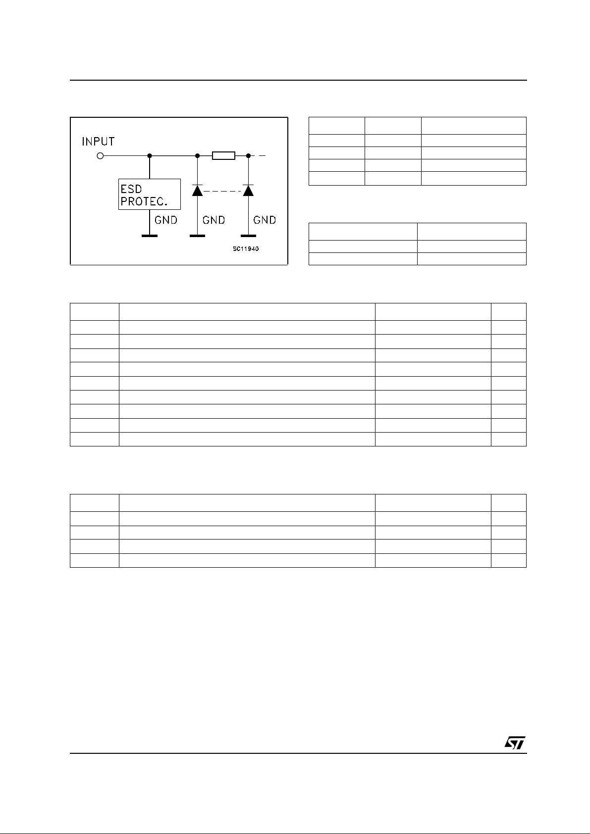
The input is equipped with protection circuits
against static discharge, giving it ESD immunity
and transient excess voltage.
PIN CONNECTION AND IEC LOGIC SYMBOLS
1/7June 2003
74V2T14
INPUT EQUIVALENT CIRCUIT PIN DESCRIPTION
PIN No SYMBOL NAME QND FUNCTION
1, 3, 6 1A, 2A, 3A Data Inputs
7, 5, 2 1Y, 2Y, 3Y Data Outputs
4 GND Ground (0V)
8
TRUTH TABLE
ABSOLUTE MAXIMUM RATINGS
Symbol Parameter Value Unit
V
V
V
I
I
OK
I
or I
I
CC
T
T
Absolute Maximum Ratings are those values beyond which damage to the device may occur. Functional operation under these conditions is
not implied.
Supply Voltage
CC
DC Input Voltage
I
DC Output Voltage -0.5 to VCC+ 0.5
O
DC Input Diode Current
IK
DC Output Diode Current
DC Output Current
O
DC VCCor Ground Current
GND
Storage Temperature
stg
Lead Temperature (10 sec)
L
V
CC
Positive Supply Voltage
AY
LH
HL
-0.5 to +7.0 V
-0.5 to +7.0 V
V
-20 mA
± 20 mA
± 25 mA
± 50 mA
-65 to +150 °C
260 °C
RECOMMENDED OPERATING CONDITIONS
Symbol Parameter Value Unit
V
V
V
T
2/7
Supply Voltage
CC
Input Voltage
I
Output Voltage 0 to V
O
Operating Temperature
op
4.5 to 5.5 V
0 to 5.5 V
CC
-55 to 125 °C
V
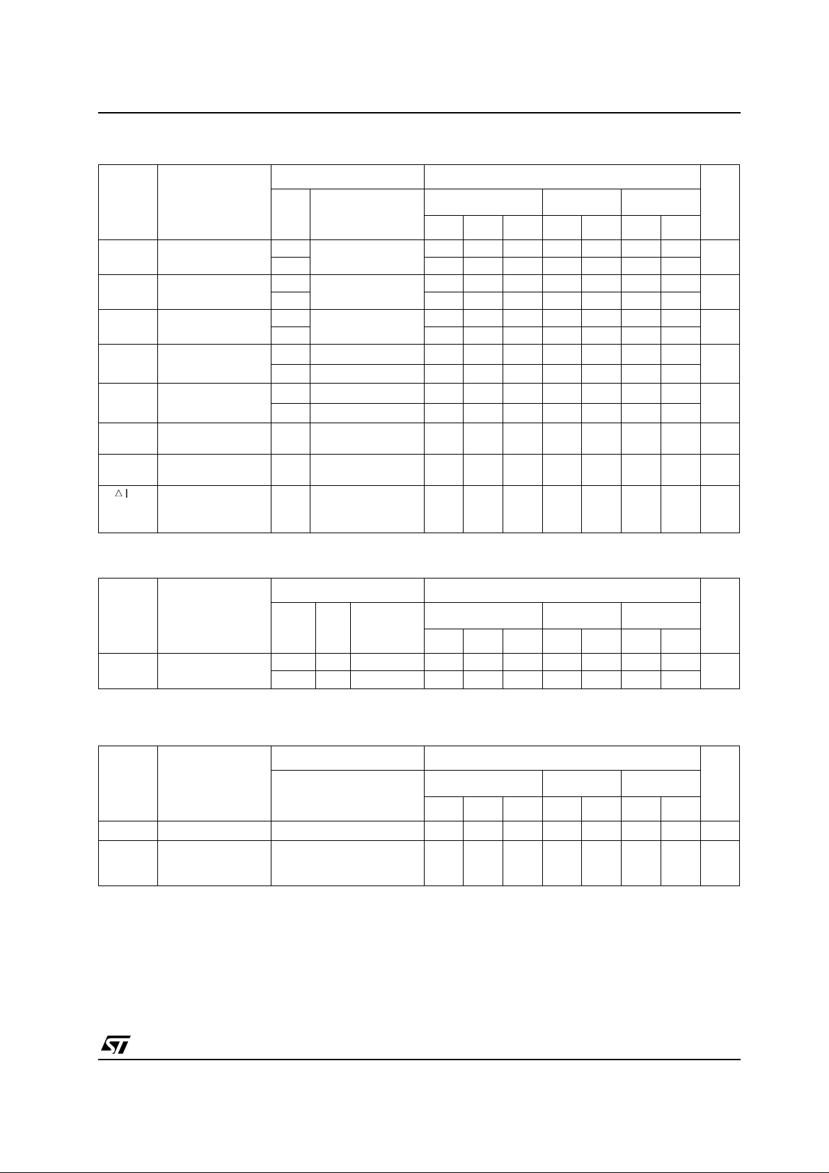
DC SPECIFICATIONS
Symbol Parameter
V
High Level
t+
Threshold Voltage
V
Low Level
t-
Threshold Voltage
V
Hysteresis Voltage 4.5 0.4 1.4 0.4 1.4 0.4 1.4
h
V
V
+
High Level Output
OH
Voltage
Low Level Output
OL
Voltage
Input Leakage
I
I
Current
Quiescent Supply
I
CC
Current
I
Additional Worst
CC
Case Supply
Current
Test Condition Value
V
(V)
CC
T
A
Min. Typ. Max. Min. Max. Min. Max.
-40 to 85°C -55 to 125°C
= 25°C
4.5 0.9 2.0 0.9 2.0 0.9 2.0
5.5 1.1 2.0 1.1 2.0 1.1 2.0
4.5 0.5 1.5 0.5 1.5 0.5 1.5
5.5 0.6 1.6 0.6 1.6 0.6 1.6
5.5 0.5 1.6 0.5 1.6 0.5 1.6
4.5
4.5
4.5
4.5
0to
5.5
5.5
5.5
IO=-50 µA 4.4 4.5 4.4 4.4 V
=-8 mA 3.94 3.8 3.7
I
O
IO=50 µA 0.0 0.1 0.1 0.1 V
=8 mA 0.36 0.44 0.55
I
O
VI= 5.5V or GND
V
I=VCC
or GND
One Input at 3.4V,
other input at V
CC
± 0.1 ± 1.0 ± 1.0 µA
11020µA
1.35 1.5 1.5 mA
or GND
74V2T14
Unit
V
V
V
AC ELECTRICAL CHARACTERISTICS (Input t
r=tf
=3ns)
Test Condition Value
Symbol Parameter
t
t
(*) Voltage range is5.0V ± 0.5V
Propagation Delay
PLH
Time
PHL
T
V
CC
(V)
C
(pF)
L
A
Min. Typ. Max. Min. Max. Min. Max.
5.0 (*) 15 5.0 7.5 1.0 9.0 1.0 10.5
5.0 (*) 50 6.5 8.5 1.0 10.0 1.0 11.5
-40 to 85°C -55 to 125°C
Unit
ns
= 25°C
CAPACITIVE CHARACTERISTICS
Test Condition Value
= 25°C
Symbol Parameter
T
A
Min. Typ. Max. Min. Max. Min. Max.
C
C
Input Capacitance
IN
Power Dissipation
PD
Capacitance
410 10 10pF
14 pF
(note 1)
1) CPDis defined as the value of the IC’s internal equivalent capacitance which is calculated from the operating current consumption without
load. (Refer to Test Circuit). Average operating current can be obtained by the following equation. I
-40 to 85°C -55 to 125°C
CC(opr)=CPDxVCCxfIN+ICC
Unit
/3
3/7
 Loading...