

查询74V2G70供应商
74V2G70
TRIPLE BUFFER
■ HIGH SPEED: t
■ LOW POWER DISSIPATION:
I
=1µA(MAX.) atTA=25°C
CC
■ HIGH NOISE IMMUNITY:
V
NIH=VNIL
■ POWER DOWN PROTECTION ON INPUTS
= 28% VCC(MIN.)
= 3.0ns (TYP.) at VCC=5V
PD
AND OUTPUTS
■ SYMMETRICAL OUTPUT IMPEDANCE:
|I
|=IOL=8mA(MIN)atVCC=4.5V
OH
II
|=IOL=4mA(MIN)atVCC=3.0V
OH
■ BALANCED PROPAGATION DELAYS:
t
≅ t
PLH
PHL
■ OPERATING VOLTAGE RANG E:
V
(OPR) = 2V to 5.5V
CC
■ IMPROVED LATCH-UP IMMUNITY
DESCRIPTION
The 74V2G70 is an advanced high-speed CMOS
TRIPLE NOT INVERTED BUFFERfabricated with
sub-micron silicon gate and double-layer metal
wiring C
2
MOS technology.
The internal circuit is composed of 3 st ages
including buffer output, w hich provide high noise
immunity and stable output.
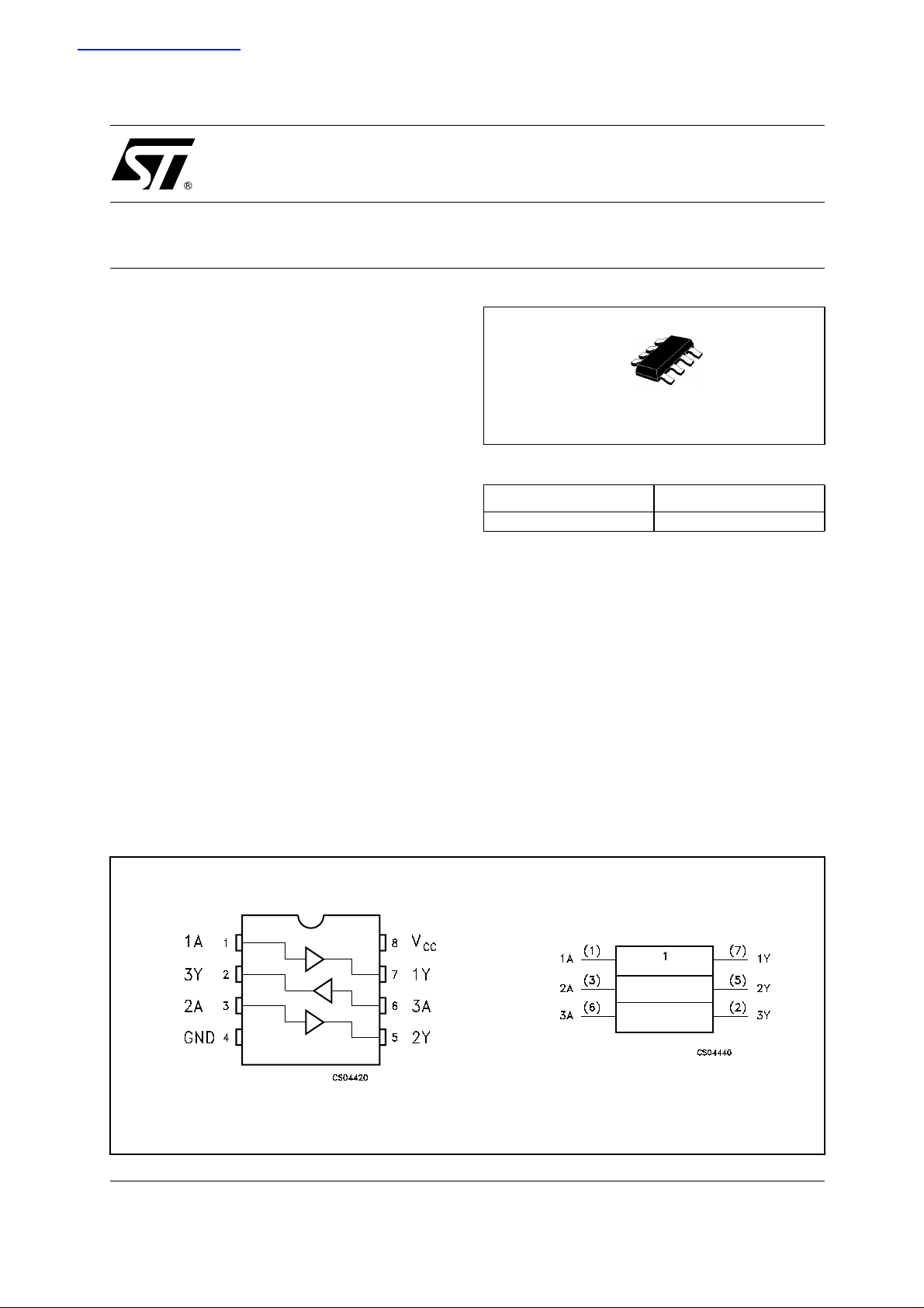
SOT23-8L
ORDER CODES
PACKAGE T & R
SOT23-8L 74V2G70STR
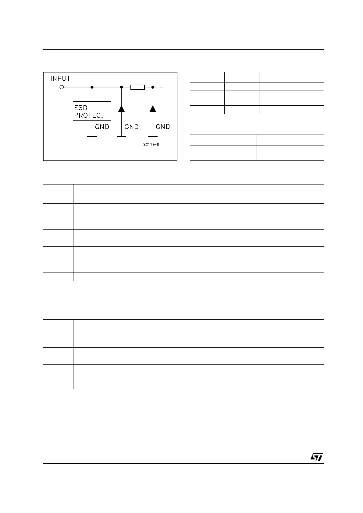
Power down protection is provided on all inputs
and outpu ts and 0 t o 7V can be accepted on
inputs with no regard to th e s upply voltage.
This device can be used to interface 5V to 3V
systems and it is ideal for portable applications
like personal digital assistant, camcorder and all
battery-powered equipment.
All inputs and outputs are equipped with
protection circuits aga inst st atic discharge, giving
them ESD immunity and transient excess voltage.
PIN CONNECTION AND IEC LOGIC SYMBOLS
1/8June 2003
74V2G70
INPUT EQUIVALENT CIRCUIT PIN DESCRIPTION
PIN No SYMBOL NAME QND FUNCTION
1, 3, 6 1A, 2A, 3A Data Inputs
7, 5, 2 1Y, 2Y, 3Y Data Outputs
4 GND Ground (0V)
8
TRUTH TABLE
ABSOLUTE MAXIMUM RATINGS
Symbol Parameter Value Unit
V
CC
V
V
V
I
IK
I
OK
I
or I
I
CC
T
stg
T
Absolute Maximum Ratings are those values beyond which damage to the device may occur. Functional operation under these conditions is
not implied.
=0V
1) V
CC
2) Highor Low State
Supply Voltage
DC Input Voltage
I
DC Output Voltage (see note 1)
O
DC Output Voltage (see note 2) -0.5 to VCC+ 0.5
O
DC Input Diode Current
DC Output Diode Current
DC Output Current
O
DC VCCor Ground Current
GND
Storage Temperature
Lead Temperature (10 sec)
L
V
CC
Positive Supply Voltage
nA nY
LL
HH
-0.5 to +7.0 V
-0.5 to +7.0 V
-0.5 to +7.0 V
V
− 20 mA
− 20 mA
± 25 mA
± 50 mA
-65 to +150 °C
260 °C
RECOMMENDED OPERATING CONDITIONS
Symbol Parameter Value Unit
V
CC
V
V
V
T
dt/dv
1) VCC=0V
2) Highor Low State
from30% to 70% ofV
3) V
IN
2/8
Supply Voltage
Input Voltage
I
Output Voltage (see note 1)
O
Output Voltage (see note 2) 0 to V
O
Operating Temperature
op
(V
CC
CC
=3.3±0.3V)
= 5.0 ± 0.5V)
Input Rise and Fall Time (note 3) (V
CC
2 to 5.5 V
0 to 5.5 V
0 to 5.5 V
CC
-55 to 125 °C
0 to 100
0to20
V
ns/V
ns/V
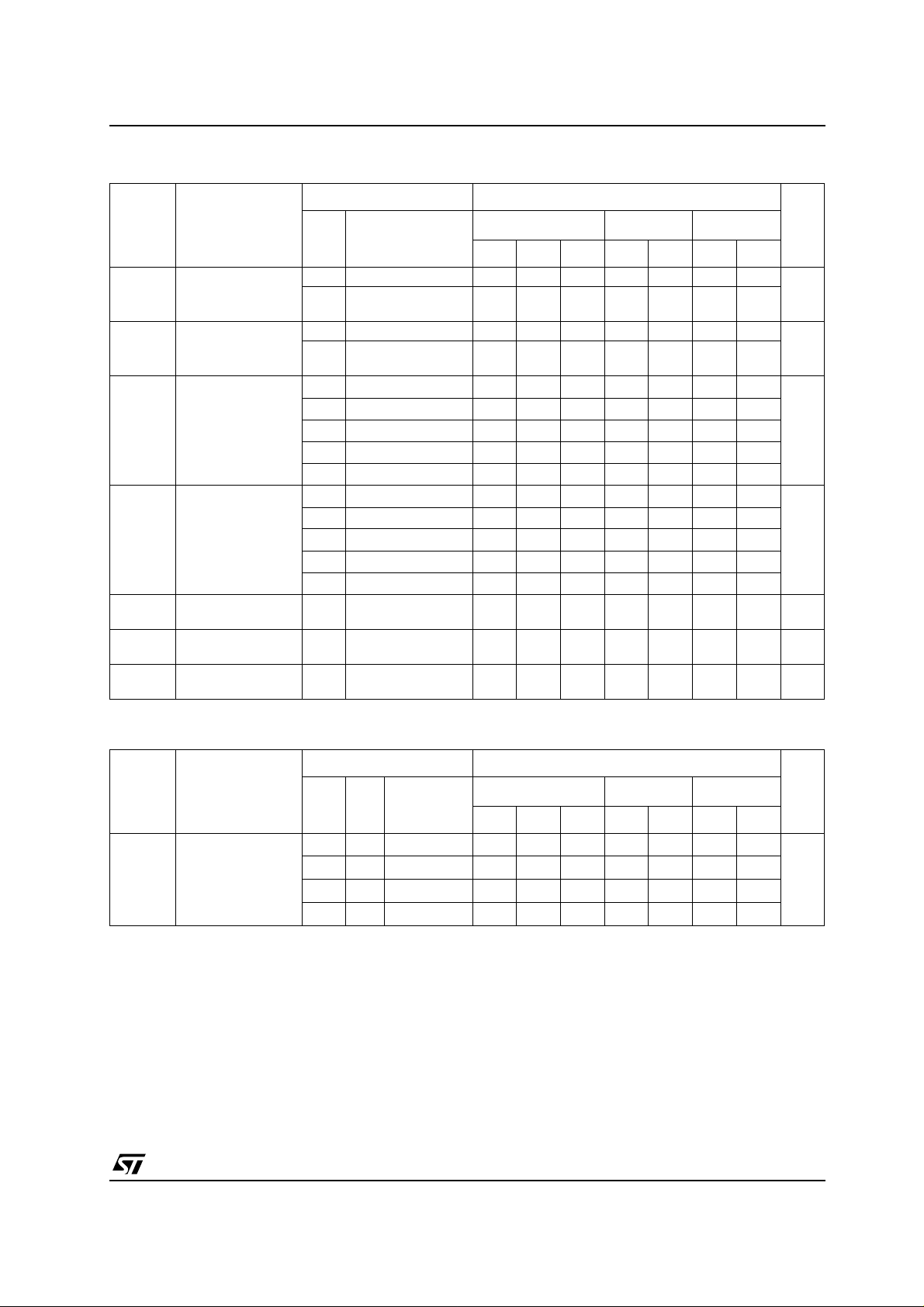
DC SPECIFICATIONS
Symbol Parameter
V
V
V
I
High Level Input
IH
Voltage
V
Low Level Input
IL
Voltage
High Level Output
OH
Voltage
Low Level Output
OL
Voltage
Input Leakage
I
I
Current
I
Quiescent Supply
CC
Current
Power downOutput
OPD
Leakage Current
Test Condition Value
V
(V)
CC
T
A
Min. Typ. Max. Min. Max. Min. Max.
-40 to 85°C -55 to 125°C
= 25°C
2.0 1.5 1.5 1.5
3.0to
5.5
0.7V
CC
0.7V
CC
0.7V
CC
2.0 0.5 0.5 0.5
3.0to
5.5
2.0
3.0
4.5
3.0
4.5
2.0
3.0
4.5
3.0
4.5
0to
5.5
5.5
0
IO=-50 µA
=-50 µA
I
O
=-50 µA
I
O
=-4 mA
I
O
=-8 mA
I
O
IO=50 µA
=50 µA
I
O
=50 µA
I
O
=4 mA
I
O
=8 mA
I
O
= 5.5V or GND
V
I
V
I=VCC
V
O
or GND
= 5.5
1.9 2.0 1.9 1.9
2.9 3.0 2.9 2.9
4.4 4.5 4.4 4.4
2.58 2.48 2.4
3.94 3.8 3.7
0.3V
CC
0.3V
CC
0.0 0.1 0.1 0.1
0.0 0.1 0.1 0.1
0.0 0.1 0.1 0.1
0.36 0.44 0.55
0.36 0.44 0.55
± 0.1 ± 1 ± 1 µA
11020µA
0.5 5 10 µA
74V2G70
Unit
0.3V
CC
V
V
V
V
AC ELECTRICAL CHARACTERISTICS (Input t
Test Condition Value
Symbol Parameter
t
PLHtPHL
(*) Voltage range is3.3V ± 0.3V
(**) Voltage range is 5.0V ± 0.5V
Propagation Delay
Time
3.3
3.3
5.0
5.0
C
V
CC
(V)
L
(pF)
(*)
15 3.7 7.0 1.0 8.0 1.0 9.0
(*)
50 5.3 8.0 1.0 9.5 1.0 10.5
(**)
15 3.0 5.0 1.0 6.0 1.0 7.0
(**)
50 4.1 6.5 1.0 7.5 1.0 8.5
=3ns)
r=tf
= 25°C
T
A
-40 to 85°C -55 to 125°C
Min. Typ. Max. Min. Max. Min. Max.
Unit
ns
3/8
 Loading...