

ST 74V2G126 User Manual
查询74V2G126供应商
74V2G126
DUAL BUS BUFFER (3-STATE)
■ HIGH SPEED: t
■ LOW POWER DISSIPATION:
= 3.8ns (TYP.) at VCC=5V
PD
ICC=1µA(MAX.) at TA=25°C
■ HIGH NOISE IMMUNITY:
V
NIH=VNIL
■ POWER DOWNPROTECTION ON INPUTS
= 28% VCC(MIN.)
AND OUTPUTS
■ SYMMETRICAL OUTPUT IMPEDANCE:
|IOH|=IOL= 8mA (MIN) at VCC= 4.5V
■ BALANCED PROPAGATION DELAYS:
t
≅ t
PLH
■ OPERATING VOLTAGE RANGE:
PHL
VCC(OPR) = 2V to 5.5V
■ IMPROVED LATCH-UP IMMUNITY
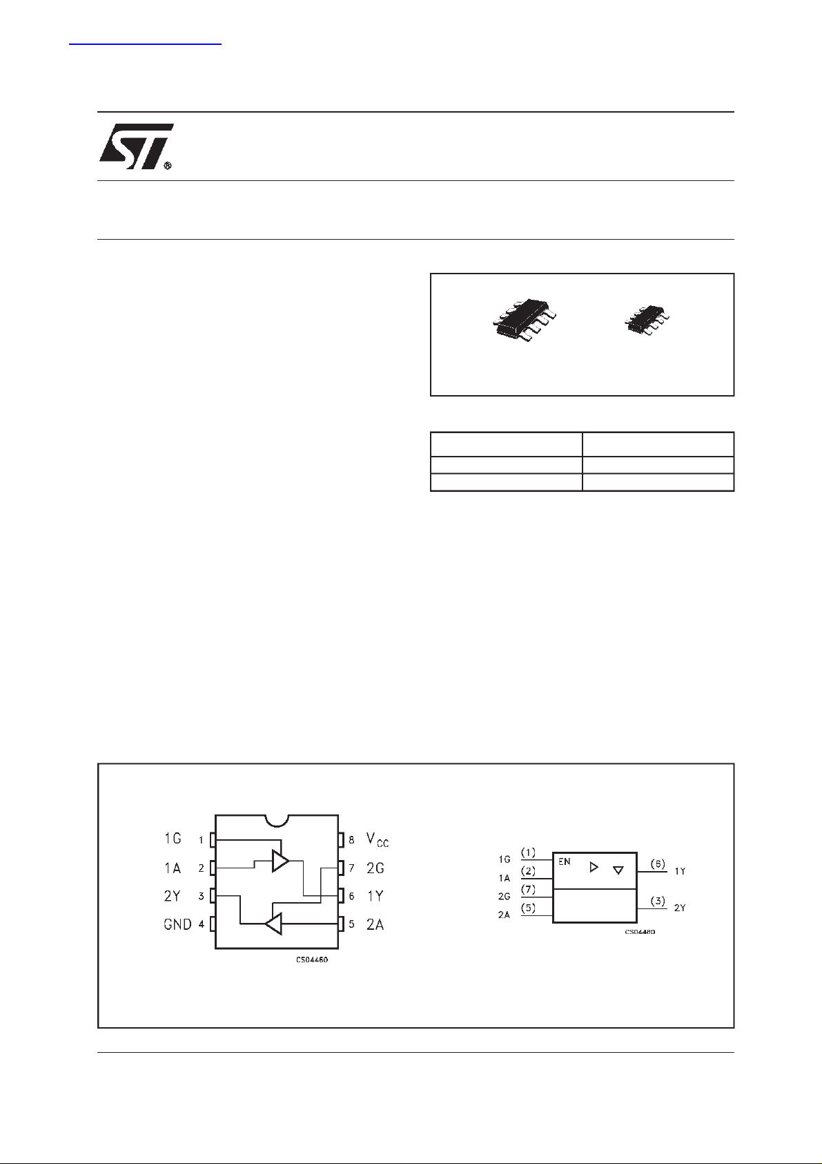
DESCRIPTION
The 74V2G126 is anadvancedhigh-speed CMOS
DUAL BUS BUFFER fabricated with sub-micron
silicon gate and double-layer metal wiring C2MOS
tecnology.
3-STATE control input nG has to be set LOW to
place the output into the high impedance state.
Power down protection is provided on all inputs
and outputs and 0 to 7V can be accepted on
SOT23-8L SOT323-8L
ORDER CODES
PACKAGE T & R
SOT23-8L 74V2G126STR
SOT323-8L 74V2G126CTR
inputs with no regard to the supply voltage. This
device can be used to interface 5V to 3V systems
and it is ideal for portable applications like
personal digital assistant, camcorder and all
battery-powered equipment.
All inputs and outputs are equipped with
protection circuits against static discharge, giving
them ESD immunity and transient excess voltage.
PIN CONNECTION AND IEC LOGIC SYMBOLS
1/11November 2001
74V2G126
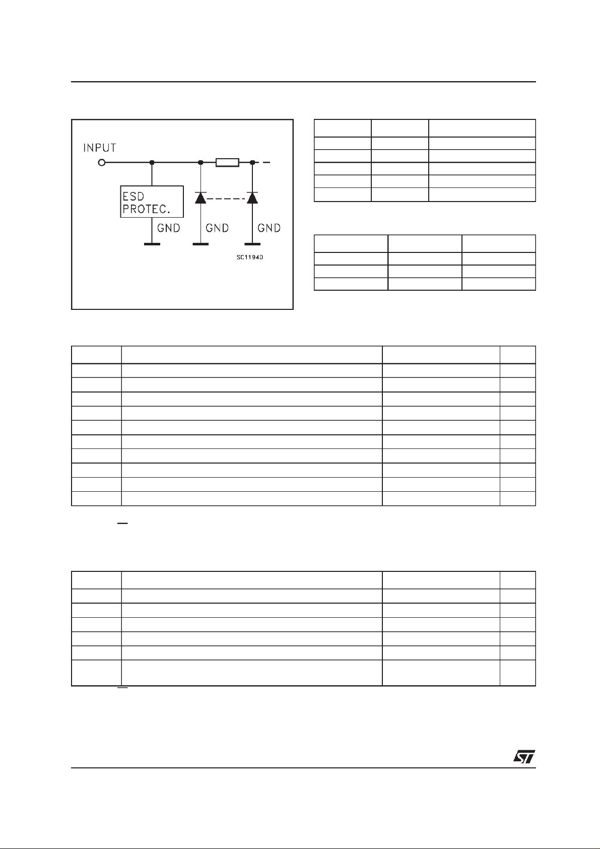
INPUT EQUIVALENT CIRCUIT PIN DESCRIPTION
PIN No SYMBOL NAME AND FUNCTION
1, 7 1G, 2G Output Enable Inputs
2, 5 1A, 2A Data Inputs
3, 6 2Y, 1Y Data Outputs
4 GND Ground (0V)
8
TRUTH TABLE
AGY
XLZ
LHL
HHH
X: ”H” or ”L”
Z: High Impedance
ABSOLUTE MAXIMUM RATINGS
Symbol Parameter Value Unit
V
V
V
V
I
I
OK
I
or I
I
CC
T
T
Absolute Maximum Ratings are those values beyond which damage to the device may occur. Functional operation under these conditions is
not implied.
1) Vcc=0V or nG=Vcc(Output in High Impedence state)
2) High or Low State
Supply Voltage
CC
DC Input Voltage
I
DC Output Voltage (see note 1)
O
DC Output Voltage (see note 2) -0.5 to VCC+ 0.5
O
DC Input Diode Current
IK
DC Output Diode Current
DC Output Current
O
DC VCCor Ground Current
GND
Storage Temperature
stg
Lead Temperature (10 sec)
L
V
CC
Positive Supply Voltage
-0.5 to +7.0 V
-0.5 to +7.0 V
-0.5 to +7.0 V
− 20 mA
− 20 mA
± 25 mA
± 50 mA
-65 to +150 °C
260 °C
V
RECOMMENDED OPERATING CONDITIONS
Symbol Parameter Value Unit
V
V
V
V
T
dt/dv
1) Vcc=0V or nG=Vcc (Output in High Impedence state)
2) High or Low State
from 30% to 70% of V
3) V
IN
2/11
Supply Voltage
CC
Input Voltage
I
Output Voltage (see note 1)
O
Output Voltage (see note 2) 0 to V
O
Operating Temperature
op
(V
CC
CC
= 3.3 ± 0.3V)
= 5.0 ± 0.5V)
Input Rise and Fall Time (note 3) (V
CC
2 to 5.5 V
0 to 5.5 V
0 to 5.5 V
CC
-55 to 125 °C
0 to 100
0to20
V
ns/V
ns/V
DC SPECIFICATION
Symbol Parameter
V
V
V
V
I
I
OPD
I
High Level Input
IH
Voltage
Low Level Input
IL
Voltage
High Level Ouput
OH
Voltage
Low Level Output
OL
Voltage
High Impedance
OZ
Output Leakage
Current
I
Input Leakage
I
Current
Power downOutput
Leakage Current
Quiescent Supply
CC
Current
Test Condition Value
V
(V)
CC
T
A
Min. Typ. Max. Min. Max. Min. Max.
-40 to 85°C -55 to 125°C
=25°C
2.0 1.5 1.5 1.5
3.0 to
5.5
0.7V
CC
0.7V
CC
0.7V
CC
2.0 0.5 0.5 0.5
3.0 to
5.5
2.0
3.0
4.5
3.0
4.5
2.0
3.0
4.5
3.0
4.5
5.5
0to
5.5
0
5.5
IO=-50 µA
=-50 µA
I
O
I
=-50 µA
O
=-4mA
I
O
=-8mA
I
O
I
=50 µA
O
=50 µA
I
O
I
=50 µA
O
=4 mA
I
O
I
=8 mA
O
I=VIH
orV
IL
V
VO= 5.5 or GND
V
= 5.5V or GND
I
V
= 5.5
O
V
I=VCC
or GND
1.9 2.0 1.9 1.9
2.9 3.0 2.9 2.9
4.4 4.5 4.4 4.4
2.58 2.48 2.4
3.94 3.8 3.7
0.3V
CC
0.3V
CC
0.0 0.1 0.1 0.1
0.0 0.1 0.1 0.1
0.0 0.1 0.1 0.1
0.36 0.44 0.55
0.36 0.44 0.55
±0.25 ± 2.5 ± 5 µA
± 0.1 ± 1 ± 1 µA
0.5 5 10 µA
11020µA
74V2G126
Unit
V
CC
V
V
V
0.3V
3/11
74V2G126
AC ELECTRICAL CHARACTERISTICS (Input tr=tf= 3ns)
Test Condition Value
Symbol Parameter
t
PLH
t
PHL
t
t
PHZ
t
t
PZH
(*) Voltage range is 3.3V ± 0.3V
(**) Voltage range is 5.0V ± 0.5V
Propagation Delay
Time
Output Disable
PLZ
Time
Output Enable
PZL
Time
3.3
3.3
5.0
5.0
3.3
3.3
5.0
5.0
3.3
3.3
5.0
5.0
C
V
CC
(V)
L
(pF)
(*)
15 5.1 7.5 1.0 8.5 1.0 9.5
(*)
50 5.6 8.0 1.0 9.5 1.0 10.5
(**)
15 3.8 5.5 1.0 6.5 1.0 7.5
(**)
50 4.3 6.5 1.0 7.5 1.0 8.5
(*)
15 RL=1KΩ 5.4 8.0 1.0 9.0 1.0 10.0
(*)
(**)
(**)
(*)
(*)
(**)
(**)
R
50
15
50
L
R
L
R
L
=1KΩ
=1KΩ
=1KΩ
15 RL=1KΩ 5.4 7.6 1.0 9.5 1.0 10.5
R
50
15
50
L
R
L
R
L
=1KΩ
=1KΩ
=1KΩ
Min. Typ. Max. Min. Max. Min. Max.
=25°C
T
A
-40 to 85°C -55 to 125°C
7.9 11.5 1.0 12.5 1.0 13.5
3.6 5.0 1.0 6.0 1.0 7.0
5.1 7.0 1.0 8.0 1.0 9.0
5.9 8.5 1.0 10.0 1.0 11.0
3.7 5.9 1.0 7.0 1.0 8.0
4.1 6.5 1.0 7.5 1.0 8.5
Unit
ns
ns
ns
CAPACITIVE CHARACTERISTICS
Test Condition Value
T
Symbol Parameter
C
C
C
Input Capacitance
IN
Output
OUT
Capacitance
Power Dissipation
PD
Capacitance
(note 1)
1) CPDis defined as the value of the IC’s internal equivalent capacitance which is calculated from the operating current consumption without
load. (Refer to Test Circuit). Average current can be obtained by the following equation. I
=25°C
A
-40 to 85°C -55 to 125°C
Min. Typ. Max. Min. Max. Min. Max.
4101010pF
6pF
14 pF
CC(opr)=CPDxVCCxfIN+ICC
/2
Unit
4/11
 Loading...