

查询74V2G03 供应商
74V2G03
DUAL 2-INPUT OPEN DRAIN NAND GATE
■ HIGH SPEED: t
■ LOW POWER DISSIPATION:
I
=1µA(MAX.) atTA=25°C
CC
■ HIGH NOISE IMMUNITY:
V
NIH=VNIL
■ POWER DOWN PROTECTION ON INPUTS
■ OPERATING VOLTAGE RANGE:
V
(OPR) = 2V to 5.5V
CC
■ IMPROVED LATCH-UP IMMUNITY
= 28% VCC(MIN.)
= 3.9ns (TYP.) at VCC=5V
PD
DESCRIPTION
The 74V2G03 is an advanced high-speed CMOS
DUAL 2-INPUT OPEN DRAIN NAND GA TE
fabricated with sub-micron silicon gate and
double-layer metal wiring C
2
MOS technology.
The internal circuit is composed of 3 stages
including buffer output, which provide high noise
immunity and stable output.
The device can, with an external pull-up resistor,
be used in wired AND configuration. This device
SOT23-8L
ORDER CODES
PACKAGE T & R
SOT23-8L 74V2G03STR
can also be used as a led driver in any other
application requiring current sink.
Power down protection is provide d on all inputs
and 0 to 7V can be accept ed on inputs with no
regard to the supply voltage. This device can be
usedto interface 5V to 3V.
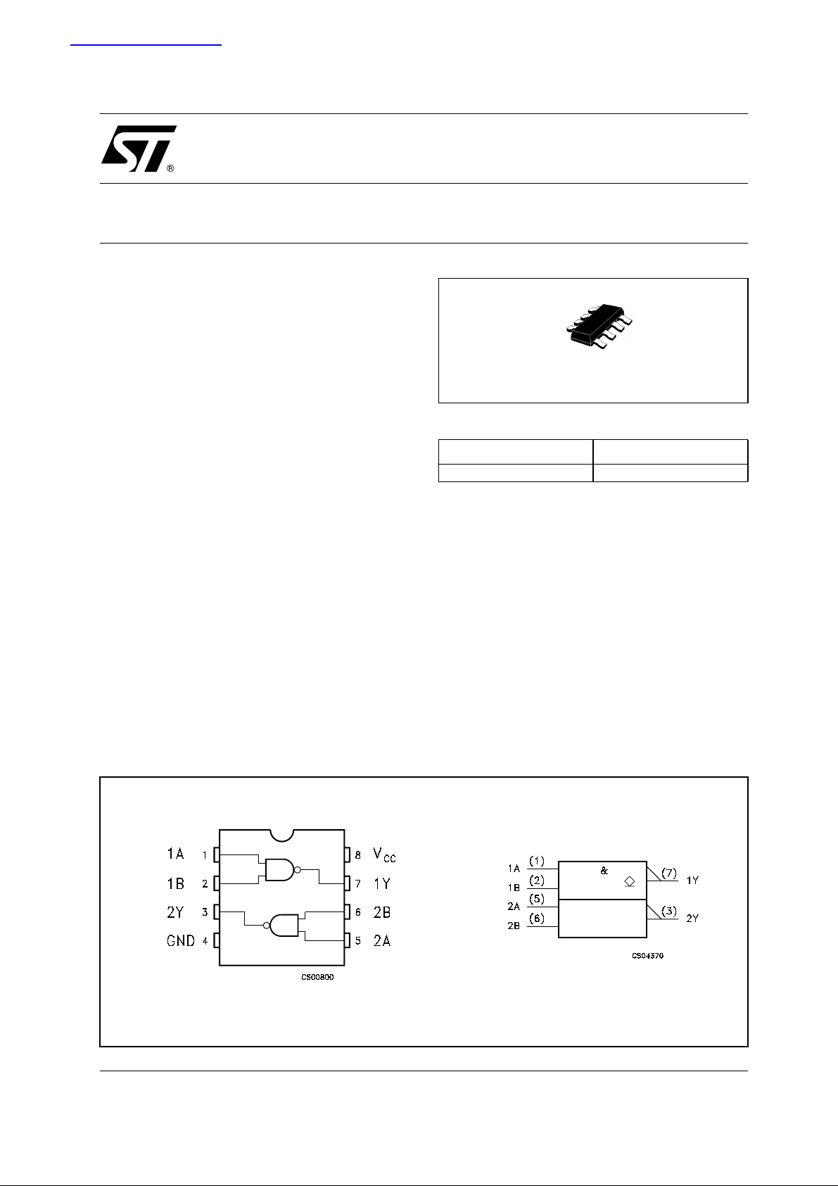
PIN CONNECTION AND IEC LOGIC SYMBOLS
1/7June 2003
74V2G03
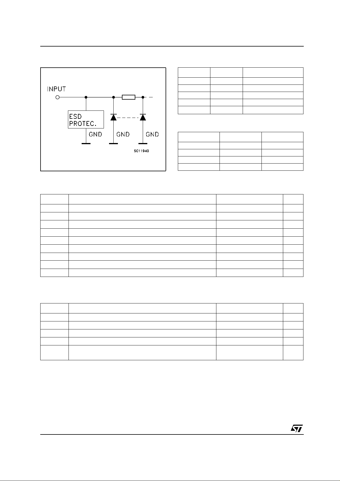
INPUT EQUIVALENT CIRCUIT PIN DESCRIPTION
PIN N° SYMBOL NAME QND FUNCTION
1, 5 1A, 2A Data Input
2, 6 1B, 2B Data Input
7, 3 1Y, 2Y Data Output
4 GND Ground (0V)
8
TRUTH TABLE
ABY
LLZ
LHZ
HLZ
HHL
Z: HighImpedance
ABSOLUTE MAXIMUM RATINGS
Symbol Parameter Value Unit
V
V
V
I
I
OK
I
or I
I
CC
T
T
Absolute Maximum Ratings are those values beyond which damage to the device may occur. Functional operation under these conditions is
not implied.
Supply Voltage
CC
DC Input Voltage
I
DC Output Voltage -0.5 to VCC+ 0.5
O
DC Input Diode Current
IK
DC Output Diode Current
DC Output Current
O
DC VCCor Ground Current
GND
Storage Temperature
stg
Lead Temperature (10 sec)
L
V
CC
Positive Supply Voltage
-0.5 to +7.0 V
-0.5 to +7.0 V
-20 mA
± 20 mA
± 25 mA
± 50 mA
-65 to +150 °C
260 °C
V
RECOMMENDED OPERATING CONDITIONS
Symbol Parameter Value Unit
V
V
V
T
dt/dv
1) VINfrom30% to 70% of V
2/7
Supply Voltage
CC
Input Voltage
I
Output Voltage 0 to V
O
Operating Temperature
op
(V
CC
CC
=3.3±0.3V)
= 5.0 ± 0.5V)
Input Rise and Fall Time (note 1) (V
CC
2 to 5.5 V
0 to 5.5 V
CC
-55 to 125 °C
0 to 100
0to20
V
ns/V
ns/V
DC SPECIFICATIONS
Symbol Parameter
V
V
High Level Input
IH
Voltage
V
Low Level Input
IL
Voltage
Low Level Output
OL
Voltage
High Impedance
I
OZ
Output Leakage
Current
Input Leakage
I
I
Current
Quiescent Supply
I
CC
Current
Test Condition Value
V
(V)
CC
T
A
Min. Typ. Max. Min. Max. Min. Max.
-40 to 85°C -55 to 125°C
= 25°C
2.0 1.5 1.5 1.5
3.0to
5.5
0.7V
CC
0.7V
CC
0.7V
CC
2.0 0.5 0.5 0.5
3.0to
5.5
2.0
3.0
4.5
3.0
4.5
5.5
0to
5.5
5.5
IO=50 µA
=50 µA
I
O
=50 µA
I
O
=4 mA
I
O
=8 mA
I
O
I=VIH
or V
IL
V
VO=VCCor GND
V
= 5.5V or GND
I
V
I=VCC
or GND
0.3V
CC
0.3V
CC
0.0 0.1 0.1 0.1
0.0 0.1 0.1 0.1
0.0 0.1 0.1 0.1
0.36 0.44 0.55
0.36 0.44 0.55
±
0.25
± 2.5 ± 5 µA
± 0.1 ± 1 ± 1 µA
11020µA
74V2G03
Unit
0.3V
CC
V
V
V
AC ELECTRICAL CHARACTERISTICS
Test Condition Value
Symbol Parameter
t
t
(*) Voltage range is3.3V ± 0.3V
(**) Voltage range is 5.0V ± 0.5V
Propagation Delay
PZL
Time
Propagation Delay
PLZ
Time
V
3.3
3.3
5.0
5.0
3.3
5.0
C
CC
(V)
L
(pF)
(*)
15 4.8 6.5 1.0 8.0 1.0 9.0
(*)
50 5.3 7.5 1.0 9.0 1.0 10.0
(**)
15 3.9 5.5 1.0 6.5 1.0 7.5
(**)
50 4.3 6.0 1.0 7.5 1.0 8.5
(*)
50 6.8 9.5 1.0 10.0 1.0 11.0
(**)
50 4.8 6.5 1.0 7.0 1.0 8.0
= 25°C
T
A
-40 to 85°C -55 to 125°C
Min. Typ. Max. Min. Max. Min. Max.
Unit
ns
ns
3/7
 Loading...