

查询74V1T80 供应商
74V1T80
SINGLE POSITIVE EDGE TRIGGERED
D-TYPE FLIP-FLOP
■ HIGH SPEED:
f
= 180MHz (TYP.) at VCC = 5V
MAX
■ LOW POWER DISSIPATION:
I
= 1µA(MAX.) at TA=25°C
CC
■ COMPATIBLE WITH TTL OUTPUTS:
V
= 2V (MIN), VIL = 0.8V (MAX)
IH
■ POWER DOWN PROTECTION ON INPUT S
■ SYMMETRICAL OUTPUT IMPEDANCE:
|I
| = IOL = 8mA (MIN) at VCC = 4.5V
OH
■ BALANCED PROPAGATION DELAYS:
t
≅ t
PLH
■ OPERATING VOL TAGE RANGE:
V
CC
■ IMPROVED LATCH-UP IMMUNITY
PHL
(OPR) = 4.5V to 5.5V
DESCRIPTION
The 74V1T80 is an advanc ed high-speed CM OS
SINGLE POSITIVE EDGE TRIGGERED D-TYPE
FLIP-FLOP WITH INVERTED OUTPUT
fabricated with sub-micron silicon gate and
double-layer metal wiring C
2
MOS technology. it is
designed to operate from 4.5V to 5.5V, making
this device ideal for portable applications.
This D-Type flip-flop is controlled by a clock input
(CK). On the positive transition of the clock, the Q
output will be set to the logic inverted sta te that
was setup at the D input.
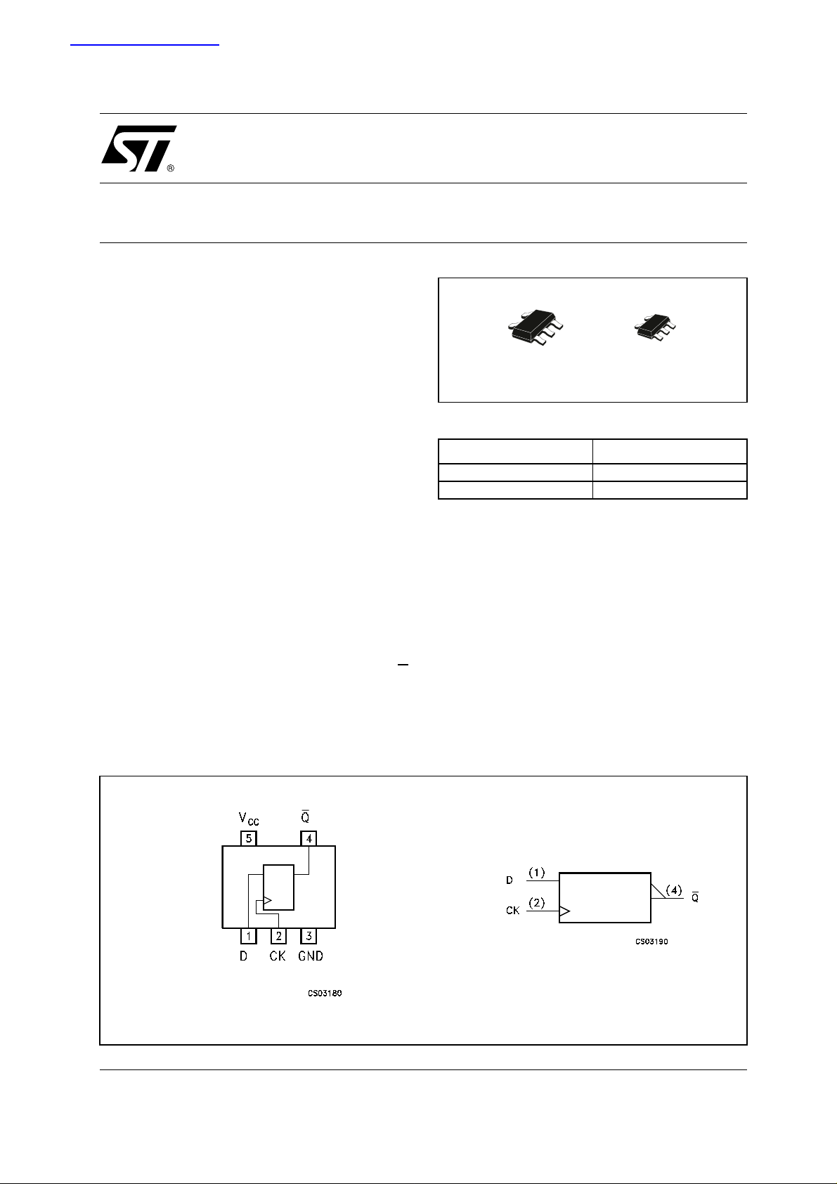
SOT323-5LSOT23-5L
ORDER CODES
PACKAGE T & R
SOT23-5L 74V1T80STR
SOT323-5L 74V1T80CTR
Following the hold time interval, data at the D input
can be changed without affecting the level at the
output. Power down protection is provided on
input and 0 to 7V can be accepted on input with no
regard to the supply voltage. This device can be
used to interface 5V to 3V.
It’s available in the commercial temperature
range. All inputs and output are equipped with
protection circuits against stat ic discharge, giving
them ESD immunity and transient excess voltage.
PIN CONNECTION AND IEC LOGIC SYMBOLS
1/9July 2001
74V1T80
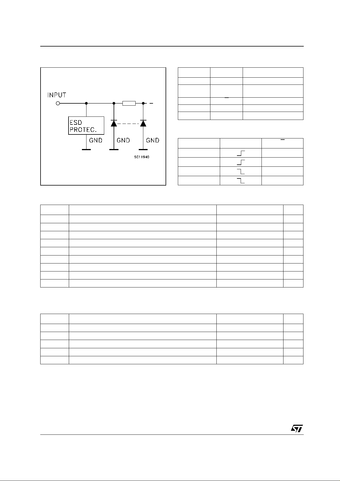
INPUT EQUIVALENT CIRCUIT PIN DESCRIPTION
PIN No SYMBOL NAME AND FUNCTION
1 D Data Input
2CK
4Q
3 GND Ground (0V)
5
TRUTH TABLE
DCKQ
LH
HL
LQn
HQn
ABSOLUTE MAXIMUM RATINGS
V
CC
Clock Input (Positive
Edge)
Inverted Flip-Flop Output
Positive Supply Voltage
Symbol Parameter Value Unit
V
V
V
I
I
OK
I
I
or I
CC
T
T
Absolute Maximum Ratings are those values beyond which damage to the device may occur. Functional operation under these conditions is
not implied
Supply Voltage
CC
DC Input Voltage
I
DC Output Voltage -0.5 to VCC + 0.5
O
DC Input Diode Current
IK
DC Output Diode Current
DC Output Current
O
DC VCC or Ground Current
GND
Storage Temperature
stg
Lead Temperature (10 sec)
L
-0.5 to +7.0 V
-0.5 to +7.0 V
V
- 20 mA
± 20 mA
± 25 mA
± 50 mA
-65 to +150 °C
300 °C
RECOMMENDED OPERATING CONDITIONS
Symbol Parameter Value Unit
V
V
V
T
dt/dv
1) VIN from 0.8V to 2V
Supply Voltage
CC
Input Voltage
I
Output Voltage 0 to V
O
Operating Temperature
op
Input Rise and Fall Time (note 1) (V
= 5.0 ± 0.5V)
CC
4.5 to 5.5 V
0 to 5.5 V
CC
-55 to 125 °C
0 to 20 ns/V
V
2/9
DC SPECIFICATIONS
Symbol Parameter
V
V
V
V
I
High Level Input
IH
Voltage
Low Level Input
IL
Voltage
High Level Output
OH
Voltage
Low Level Output
OL
Voltage
I
Input Leakage
I
Current
Quiescent Supply
CC
Current
I
Additional Worst
CC
Case Supply
Current
Test Condition Value
T
= 25°C
V
CC
(V)
4.5 to
A
Min. Typ. Max. Min. Max. Min. Max.
222V
5.5
4.5 to
5.5
4.5
4.5
4.5
4.5
0 to
5.5
5.5
IO=-50 µA 4.4 4.5 4.4 4.4 V
I
=-8 mA 3.94 3.8 3.7
O
IO=50 µA 0.0 0.1 0.1 0.1 V
I
=8 mA 0.36 0.44 0.55
O
V
= 5.5V or GND
I
= VCC or GND
V
I
One Input at 3.4V,
other input at V
5.5
CC
or GND
74V1T80
-40 to 85°C -55 to 125°C
0.8 0.8 0.8 V
± 0.1 ± 1.0 ± 1.0 µA
11020µA
1.35 1.5 1.5 mA
Unit
AC ELECTRICAL CHARACTERISTICS (Input t
= tf = 3ns)
r
Test Condition Value
Symbol Parameter
t
PLH tPHL
f
MAX
(*) Vol tage range is 5.0V ± 0.5V
Propagation Delay
Time CK to Q
CK Pulse Width,
t
W
HIGH or LOW
t
Setup Time D to
s
CK, HIGH or LOW
t
Hold Time D to CK,
h
HIGH or LOW
Maximum Clock
Frequency
= 25°C
V
(V)
CC
C
(pF)
L
A
Min. Typ. Max. Min. Max. Min. Max.
5.0 (*) 15 4.9 8.4 1.0 9.8 1.0 10.8 ns
5.0 (*) 50 5.9 12.0 1.0 14.0 1.0 15.0
5.0 (*) 50 4.0 4.0 4.0 ns
5.0 (*) 50 4.0 4.0 4.0 ns
5.0 (*) 50 1.0 1.0 1.0 ns
5.0 (*) 50
165 180 150 150
-40 to 85°C -55 to 125°C
Unit
MHz
T
CAPACITIVE CHARACTERISTICS
Test Condition Value
T
Symbol Parameter
C
C
Input Capacitance
IN
Power Dissipation
PD
Capacitance
(note 1)
1) CPD is defined as the value of the IC’s internal equivalent capacitance which is calculated from the operating current consumption without
load. (R ef er to Test Circ ui t). Average operating current can be obtained by the following equa tion. I
= 25°C
A
-40 to 85°C -55 to 125°C
Min. Typ. Max. Min. Max. Min. Max.
4101010pF
8pF
= CPD x VCC x fIN + I
CC(opr)
CC
Unit
3/9
 Loading...