

ST 74V1T384 User Manual
查询74V1T384 供应商
74V1T384
SINGLE HIGH SPEED BUS SWITCH
■ HIGH SPEED: t
■ LOW POWER DISSIPATION:
I
= 1µA(MAX.) at TA=25°C
CC
■ LOW "ON" RESISTANCE at V
R
= 7Ω (TYP) , VIN=0V, I
ON
R
= 14Ω (TYP), VIN=2.4V , I
ON
■ OPERATING VOLATGE RANGE:
V
(OPR.) = 4.0V TO 5.5V
CC
■ 5V TOLERANT ON CONTROL PIN
■ COMPA TIBLE WITH TT L OU TP U TS:
V
= 2V (MIN), VIL = 0.8V (MAX)
IH
= 0.5ns (TYP.) at VCC = 5V
PD
=5.0V:
CC
=30mA
I/O
=15mA
I/O
DESCRIPTION
The 74V1T384 is an advanced high-speed CMOS
SINGLE HIGH SPEED BUS SWITCH fabricated
in silicon gate C
2
MOS technology. It’s designed
to operate from 4V to 5.5V, making this device
ideal for portable applications. It’s offers 7Ω
Resistance typical value at V
key feature are fast switching speed (t
t
=3.3ns Typical) and Low Power
OFF
=5V. Additional
CC
=3.8ns,
ON
Consumption.
The OE
switch is ON when the OE
OFF when OE
input is provided to control the switch; the
input is held low and
is held high.
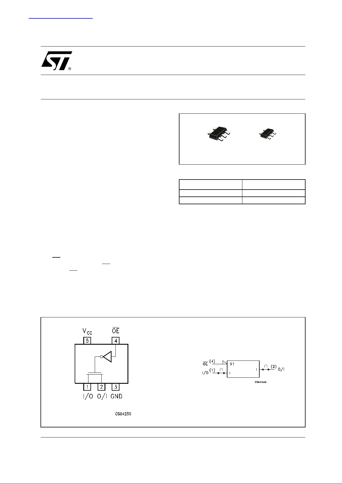
SOT323-5LSOT23-5L
ORDER CODES
PACKAGE T & R
SOT23-5L 74V1T384STR
SOT323-5L 74V1T384CTR
It’s available in the commercial and extended
temperature range in SOT23-5L and SC-70-5L
package.
PIN CONNECTION AND IEC LOGIC SYMBOLS
1/9April 2002
74V1T384
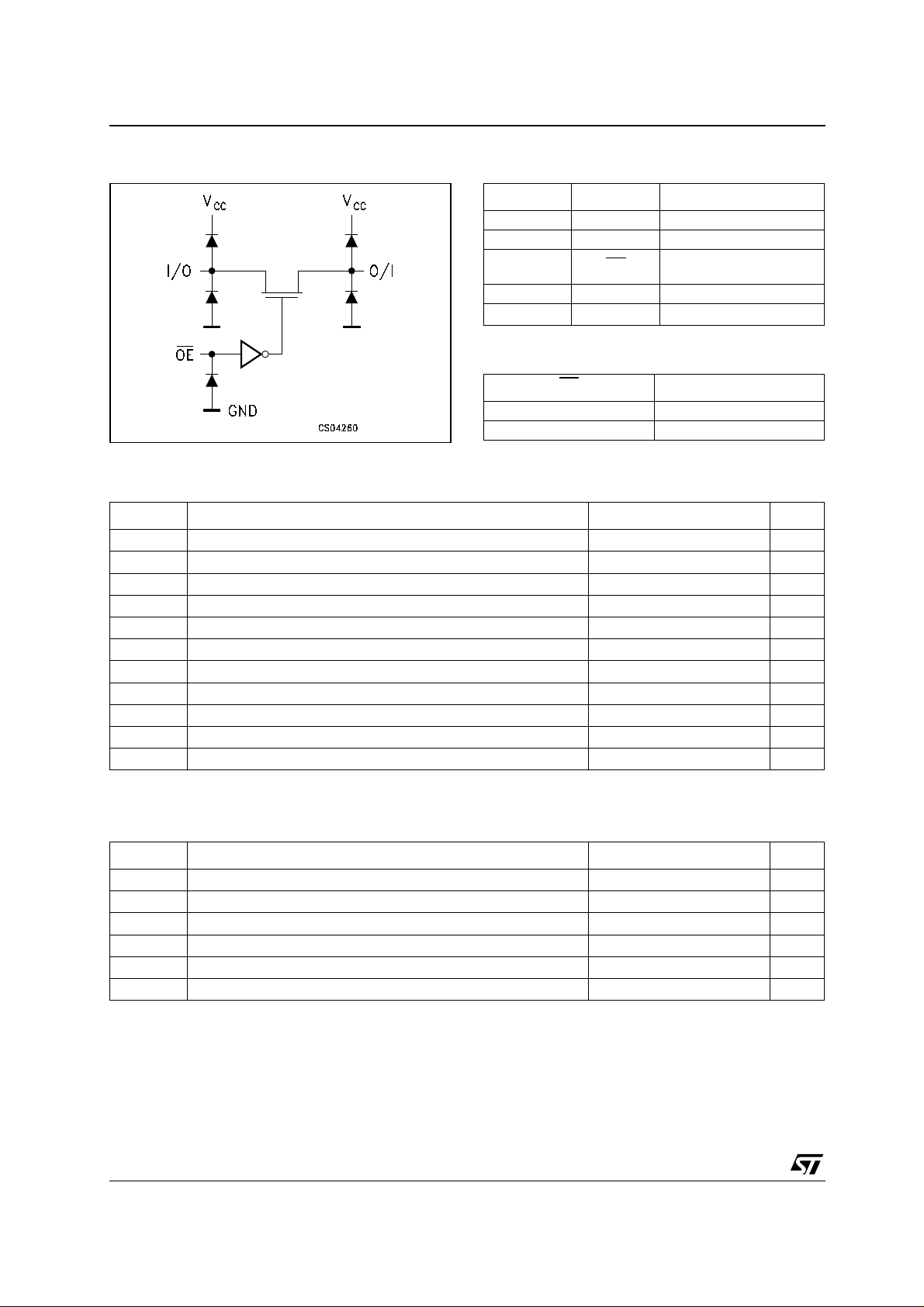
INPUT EQUIVALENT CIRCUIT PIN DESCRIPTION
PIN No SYMBOL NAME AND FUNCTION
1 I/O Independent Input/Output
2 O/I Independent Output/Input
4OE
3 GND Ground (0V)
5
TRUTH TABLE
V
CC
Enable Input (Active
HIGH)
Positive Supply Voltage
OE
SWITCH FUNCTION
LON
H OFF *
* High Impedance State
ABSOLUTE MAXIMUM RATINGS
Symbol Parameter Value Unit
V
V
V
V
I
I
I
OK
I
I
or I
CC
T
T
Absolute Maximum Ratings are those values beyond which damage to the device may occur. Functional operation under these conditions is
not implied
Supply Voltage
CC
DC Input Voltage -0.5 to VCC + 0.5
I
DC Control Input Voltage
IC
DC Output Voltage -0.5 to VCC + 0.5
O
DC Input Diode Current
IK
DC Control Input Diode Current
IK
DC Output Diode Current
DC Output Current
O
DC VCC or Ground Current
GND
Storage Temperature
stg
Lead Temperature (10 sec)
L
-0.5 to +7.0 V
-0.5 to +7.0 V
20 mA
±
- 20 mA
20 mA
±
50 mA
±
50 mA
±
-65 to +150 °C
300 °C
V
V
RECOMMENDED OPERATING CONDITIONS
Symbol Parameter Value Unit
V
V
V
V
T
dt/dv
1) VIN from 0.8V to 2V on control pin
Supply Voltage
CC
Input Voltage 0 to V
I
Control Input Voltage
IC
Output Voltage 0 to V
O
Operating Temperature
op
Input Rise and Fall Time (note 1) V
CC
= 5.0V
4.0 to 5.5 V
CC
0 to 5.5 V
CC
-55 to 125 °C
0 to 20 ns/V
2/9
V
V
DC SPECIFICATIONS
Symbol Parameter
V
V
V
V
R
R
I
I
(*) Vol tage range is 5V ± 0.5V
High Level Input
IH
Voltage
Low Level Input
IL
Voltage
High Level Input
IH
Voltage
Low Level Input
IL
Voltage
ON Resistance
ON
ON Resistance
ON
Input/Output
OFF
Leakage Current
(SWITCH OFF)
I
Control Input
IN
Leakage Current
Quiescent Supply
CC
Current
Additional Worst
I
CC
Case Supply
Current
Test Condition Value
T
= 25°C
V
5.0
5.0
CC
(V)
(*)
(*)
4.0
A
Min. Typ. Max. Min. Max. Min. Max.
222V
222V
4.0
71015
20 40 60
4.5
4.5
VIC = VIL
V
= GND
I/O
I
≤ 30 mA
I/O
VIC = VIL
V
= 2.4V
I/O
I
≤ 10 mA
I/O
VOS = VCC to GND
V
5.5
0 to
5.5
5.5
5.5 C
= VCC to GND
IS
V
= V
IC
V
= 5.5V or GND
IC
= VCC or GND
V
I
Input at 3.4V
IH
±
74V1T384
-40 to 85°C -55 to 125°C
0.8 0.8 0.8 V
0.8 0.8 0.8 V
±
0.1
0.1
±
1
±
1.0
11020
1.35 1.5 1.5 mA
10µA
±
1.0µA
±
Unit
Ω
Ω
A
µ
AC ELECTRICAL CHARACTERISTICS (CL = 50pF, Input tr = tf = 3ns)
Test Condition Value
T
Symbol Parameter
t
t
t
t
t
(*) Vol tage range is 5.0V
PD
PLZ
PHZ
PZL
PZH
Delay Time
Output Disable
Time
Output Enable
Time
±
0.5V
V
5.0
5.0
5.0
(V)
CC
(*)
tr = tf = 6ns
CL = 50pF
(*)
= 500 Ω
R
1
VIN=2.4V
CL = 50pF
(*)
= 1KΩ
R
1
VIN=2.4V
= 25°C
A
Min. Typ. Max. Min. Max. Min. Max.
0.5 0.8 1.0 2.0 ns
3.8 6.5 9.0 10.0 ns
3.3 5.0 7.5 8.5 ns
-40 to 85°C -55 to 125°C
Unit
3/9
 Loading...