

ST 74V1T32 User Manual
查询74V1T32供应商
■ HIGHSPEED:t
■ LOW POWERDISSIPAT ION:
=1 µA (MAX.) at TA=25oC
I
CC
■ COMPATIBLEWITHTTLOUTPUTS:
V
=2V(MIN),VIL=0.8V(MAX)
IH
■ POWERDOWN PROTECTIONON INPUTS&
=5 ns(TYP.)atVCC=5V
PD
OUTPUT
■ SYMMETRICALOUTPUT IMPEDANCE:
|I
|=IOL=8 mA(MIN)
OH
■ BALANCEDPROPAGATIONDELAYS:
t
≅ t
PLH
PHL
■ OPERATINGVOLTAGERANGE:
(OPR)= 4.5Vto 5.5V
V
CC
■ IMPROVEDLATCH-UP IMMUNITY
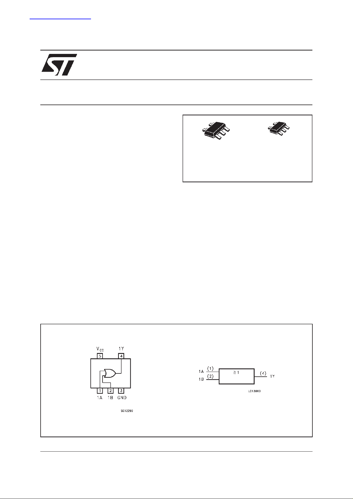
DESCRIPTION
The 74V1T32 is an advancedhigh-speed CMOS
SINGLE 2-INPUT OR GATE fabricated with
sub-micron silicon gate and double-layer metal
wiringC
2
MOStechnology.
74V1T32
SINGLE 2-INPUT OR GATE
S
(SOT23-5L)
ORDERCODE:
74V1T32S 74V1T32C
The internal circuit is composed of 2 stages
including buffer output, which provide high noise
immunityand stableoutput.
Power down protection is provided on all inputs
and 0 to 7V can be accepted on inputs with no
regard to the supply voltage. This device can be
used to interface 5V to 3V.
C
(SC-70)
PIN CONNECTION AND IEC LOGIC SYMBOLS
October 1999
1/7
74V1T32
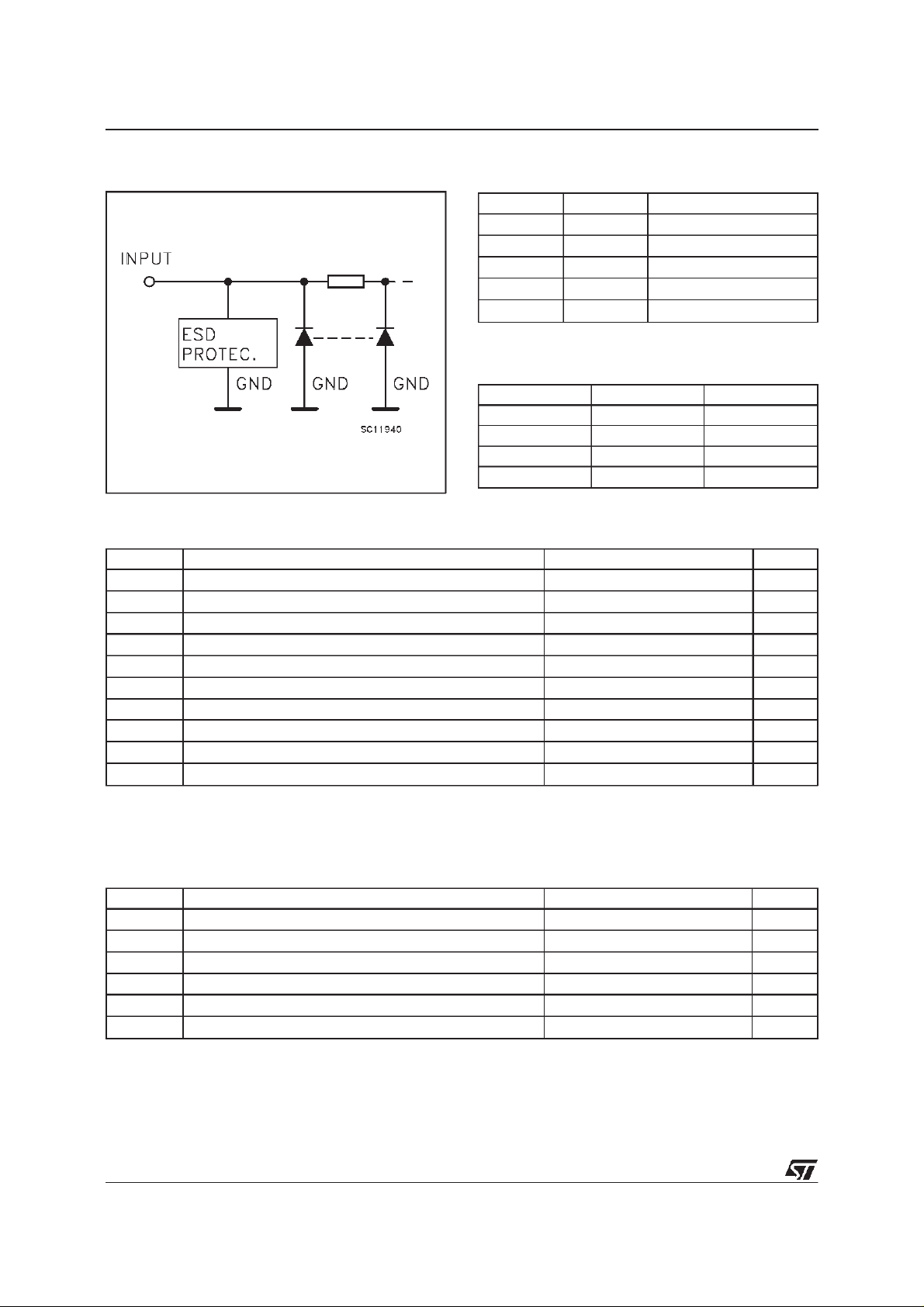
INPUT EQUIVALENTCIRCUIT
PIN DESCRIPTION
PI N No SYMB OL NAME AND FUNCTION
1 1A Data Input
2 1B Data Input
4 1Y Data Output
5 GND Ground (0V)
3V
CC
Positive Supply Voltage
TRUTH TABLE
ABY
LLL
LHH
HLH
HHH
ABSOLUTE MAXIMUM RATINGS
Symb o l Para met er Val u e Uni t
V
V
V
V
I
I
OK
I
or I
I
CC
T
T
AbsoluteMaximumRatingsarethosevaluesbeyondwhichdamagetothedevicemayoccur. Functional operation underthese conditionisnot implied.
1)V
=0V
CC
2)HighorLowState
Supply Voltage -0.5 to +7.0 V
CC
DC Input Voltage -0.5 to +7.0 V
I
DC Output Voltage (see note 1) -0.5 to +7.0 V
O
DC Output Voltage (see note 2) -0.5 to VCC+ 0.5 V
O
DC Input Diode Current - 20 mA
IK
DC Output Diode Current ± 20 mA
DC Output Current ± 25 mA
O
DC VCCor Ground Current ± 50 mA
GND
Storage Temperature -65 to +150
stg
Lead Temperature (10 sec) 260
L
o
C
o
C
RECOMMENDED OPERATINGCONDITIONS
Symb o l Para met er Value Un it
V
V
V
V
T
dt/dv Input Rise and Fall Time (see note 3) (V
1)VCC=0V
2)HighorLowState
from0.8Vto 2 V
3)V
IN
2/7
Supply Voltage 4.5 to 5.5 V
CC
Input Voltage 0 to 5.5 V
I
Output Voltage (see note 1) 0 to 5.5 V
O
Output Voltage (see note 2) 0 to V
O
Operating Temperature -40 to +85
op
=5.0±0.5V) 0 to 20 ns/V
CC
CC
V
o
C
74V1T32
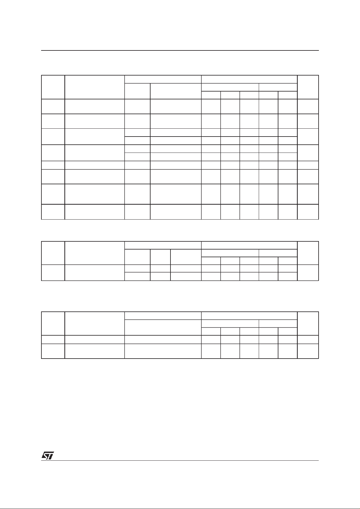
DC SPECIFICATIONS
Symb o l Para met er Test Conditio ns Val u e Uni t
=25oC -40 t o 85oC
T
A
Min. Typ. Max. Min. Max.
0.1
±
1.0
±
1.35 1.5 mA
µ
V
V
V
V
I
∆
I
OPD
V
CC
(V)
High Level Input
IH
4.5 to 5.5 2 2 V
Voltage
Low Level Input
IL
4.5 to 5.5 0.8 0.8 V
Voltage
High Level Output
OH
Voltage
Low Level Output
OL
Voltage
Input Leakage Current 0 to 5.5 VI= 5.5V or GND
I
I
Quiescent Supply
CC
4.5 IO=-50 µA 4.4 4.5 4.4
4.5 I
4.5 IO=50 µA 0.0 0.1 0.1
4.5 I
5.5 VI=VCCorGND 1 10 µA
Current
Additional Worst Case
I
CC
Supply Current
Output Leakage
5.5 One Input at 3.4V,
other input at V
0V
Current
=-8 mA 3.94 3.8
O
=8 mA 0.36 0.44
O
or
CC
GND
= 5.5V 0 0.5 5.0 µA
OUT
V
V
A
AC ELECTRICAL CHARACTERISTICS (Inputtr=tf=3 ns)
Symbol Parameter Test Conditi on Value Unit
t
Propagation Delay
PLH
t
Time
PHL
(*)Voltagerangeis5V ±0.5V
V
(*)
CC
(V)
C
(pF)
L
5.0 15 5.0 7.0 1.0 8.0
5.0 50 5.5 8.0 1.0 9.0
T
=25oC -40 t o 85oC
A
Min. Typ. Max. Min. Max.
ns
CAPACITIVE CHARACTERISTICS
Symb o l Para met er Test Conditio ns Val u e Uni t
=25oC -40 t o 85oC
T
A
Min. Typ. Max. Min. Max.
Input Capacitance 4 10 10
C
IN
Power Dissipation
C
PD
12 pF
Capacitance (note 1)
1)CPDisdefined asthevalue oftheIC’sinternal equivalentcapacitance whichiscalculatedfromtheoperatingcurrentconsumption withoutload.(Referto
TestCircuit).Average operatingcurrent canbeobtained bythefollowingequation.I
(opr)= CPD• VCC•fIN+I
CC
CC
pF
3/7
 Loading...