

查询74V1T14供应商
■ HIGHSPEED:t
■ LOW POWERDISSIPATION:
=1 µA (MAX.) at TA=25oC
I
CC
■ TYPICALHYSTERESIS:V
■ POWERDOWNPROTECTIONON INPUT
■ SYMMETRICALOUTPUTIMPEDANCE:
|I
|=IOL=8 mA(MIN)
OH
■ BALANCEDPROPAGATIONDELAYS:
t
≅ t
PLH
PHL
■ OPERATINGVOLTAGERANGE:
V
(OPR)= 4.5Vto 5.5V
CC
■ IMPROVEDLATCH-UP IMMUNITY
=4.7ns (TYP.)atVCC=5V
PD
=0.7VATVCC=4.5V
h
DESCRIPTION
The 74V1T14 is an advanced high-speed CMOS
SINGLE SCHMITT INVERTER fabricated with
sub-micron silicon gate and double-layer metal
wiringC
2
MOStechnology.
The internal circuit is composed of 3 stages
including buffer output, which provide high noise
immunityand stable output.
Power down protection is provided on input and 0
to 7V can be acceptedon inputwith no regard to
the supply voltage. This device can be used to
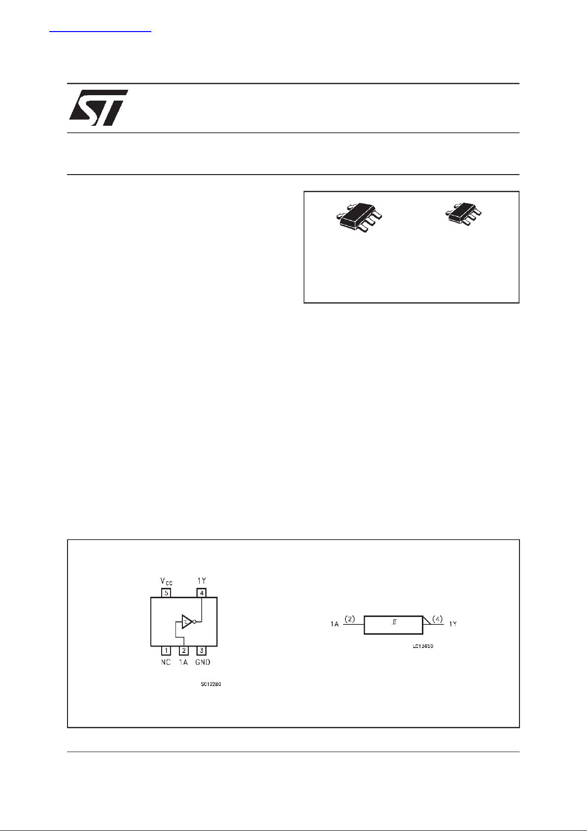
74V1T14
SINGLE SCHMITT INVERTER
S
(SOT23-5L)
ORDERCODE:
74V1T14S 74V1T14C
interface5V to 3V.
Pin configuration and function are the same as
those of the V1G04 but the V1G14 has
hysteresis.
The schmitt trigger function allows it to be used
on line receivers with slow rise/fall input signals.
C
(SC-70)
PIN CONNECTION AND IEC LOGIC SYMBOLS
October 1999
1/7
74V1T14
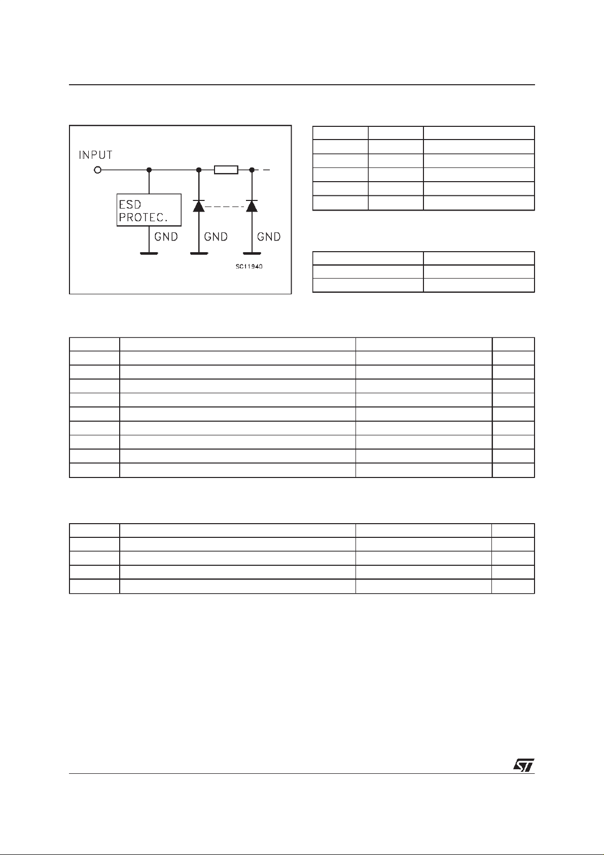
INPUT EQUIVALENTCIRCUIT
PIN DESCRIPTION
PI N No SYMB OL NAME AND FUNCTI O N
1 N.C. Not Connected
2 1A Data Input
4 1Y Data Output
3 GND Ground (0V)
5V
CC
Positive Supply Voltage
TRUTH TABLE
AY
LH
HL
ABSOLUTE MAXIMUM RATINGS
Symb o l Para met er Val u e Uni t
V
V
V
I
I
OK
I
or I
I
CC
T
T
AbsoluteMaximumRatingsarethosevaluesbeyondwhichdamagetothedevicemayoccur. Functionaloperationunder thesecondition isnotimplied.
Supply Voltage -0.5 to +7.0 V
CC
DC Input Voltage -0.5 to +7.0 V
I
DC Output Voltage -0.5 to VCC+ 0.5 V
O
DC Input Diode Current - 20 mA
IK
DC Output Diode Current
DC Output Current ± 25 mA
O
DC VCCor Ground Current ± 50 mA
GND
Storage Temperature -65 to +150
stg
Lead Temperature (10 sec) 260
L
20 mA
±
o
C
o
C
RECOMMENDEDOPERATINGCONDITIONS
Symb o l Para met er Value Un it
V
V
V
T
2/7
Supply Voltage 4.5 to 5.5 V
CC
Input Voltage 0 to 5.5 V
I
Output Voltage 0 to V
O
Operating Temperature -40 to +85
op
CC
V
o
C
74V1T14
DC SPECIFICATIONS
Symb o l Para met er Test Condit i o ns Val u e Uni t
T
V
CC
(V)
High Level Input
V
t+
Voltage
Low Level Input
V
t-
Voltage
Hysteresis Voltage 4.5 0.4 1.4 0.4 1.4
V
h
4.5 2.0 2.0
5.5 2.0 2.0
4.5 0.6 0.6
5.5 0.6 0.6
Min. Typ. Max. Min. Max.
5.5 0.4 1.5 0.4 1.5
High Level Output
V
OH
Voltage
Low Level Output
V
OL
Voltage
Input Leakage Current 0 to 5.5 VI= 5.5V or GND ±0.1 ±1.0 µA
I
I
Quiescent Supply
I
CC
4.5 IO=-50µA 4.4 4.5 4.4
4.5 I
=-8 mA 3.94 3.8
O
4.5 IO=50 µA 0.0 0.1 0.1
4.5 I
=8 mA 0.36 0.44
O
5.5 VI=VCCorGND 1 10 µA
Current
∆I
Additional Worst Case
CC
Supply Current
5.5 One Input at 3.4V,
other input at V
CC
or
GND
=25oC -40 to 85oC
A
1.35 1.5 mA
V
V
V
V
V
AC ELECTRICAL CHARACTERISTICS
(Inputt
r=tf
=3 ns)
Symbol Parameter Test Condition Value Unit
(*)
t
Propagation Delay
PLH
t
Time
PHL
(*)Voltagerangeis5V ± 0.5V
V
CC
(V)
CL
(pF)
5.0 15 5.0 7.5 1.0 9.0
5.0
50
TA=25oC -40 to 85oC
Min. Typ. Max. Min. Max.
6.5 8.5 1.0 10.0
ns
CAPACITIVE CHARACTERISTICS
Symb o l Para met er Test Condit i o ns Val u e Uni t
=25oC -40 to 85oC
T
A
Min. Typ. Max. Min. Max.
Input Capacitance 4 10 10 pF
C
IN
Power Dissipation
C
PD
Capacitance (note 1)
1)CPDisdefinedasthevalueoftheIC’sinternal equivalent capacitance whichiscalculated fromtheoperatingcurrentconsumptionwithout load.(Referto
TestCircuit).Averageoperatingcurrent canbe obtainedbythefollowingequation.I
(opr)= CPD• VCC• fIN+I
CC
12 pF
CC
3/7
 Loading...