

74V1T08
SINGLE 2-INPUT AND GATE
■ HIGH SPEED: t
■ LOW POWER DISSIPATION:
I
=1µA(MAX.) at TA=25°C
CC
■ COMPATIBLE WITHTTL OUTPUTS:
V
=2V(MIN),VIL=0.8V(MAX)
IH
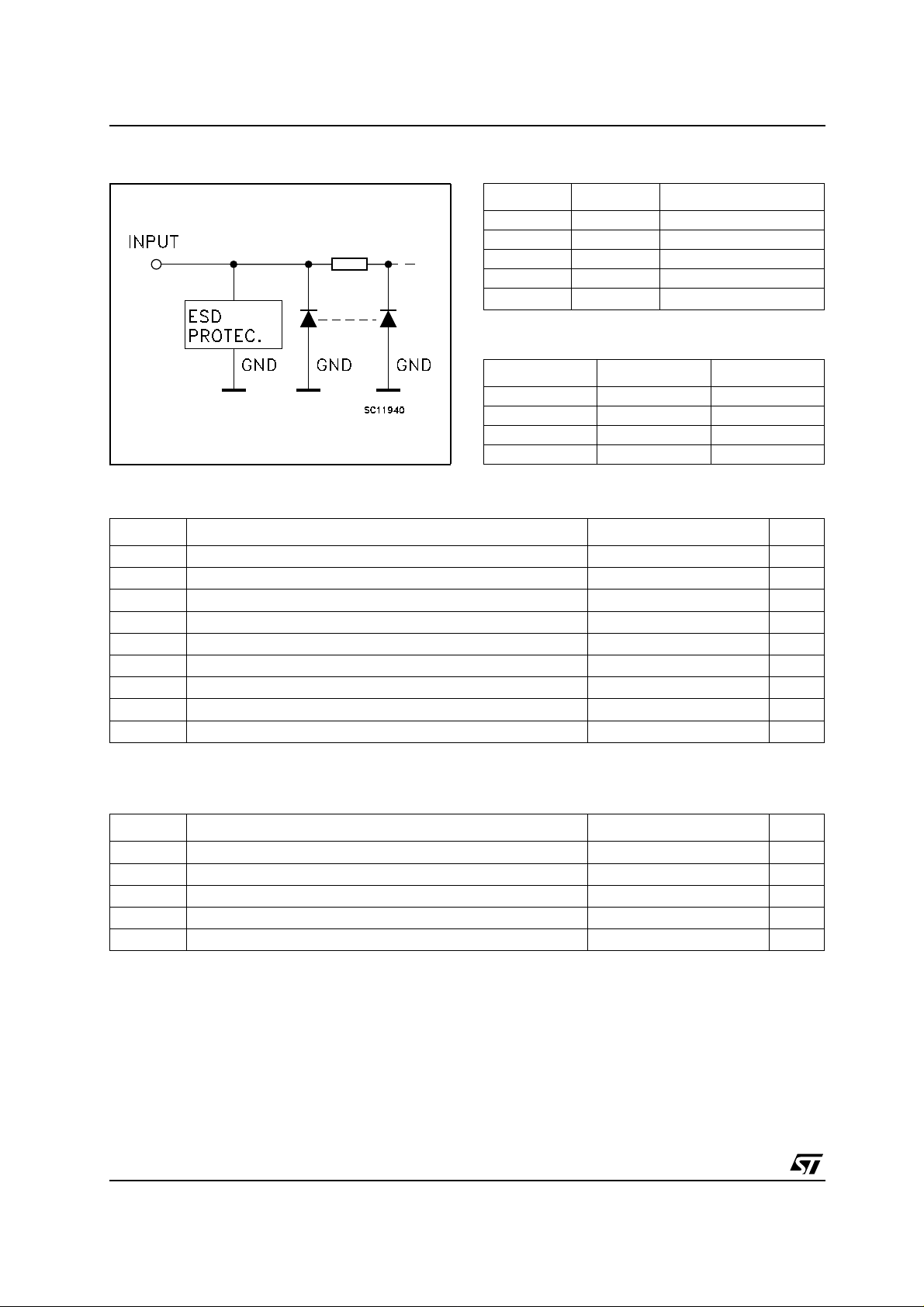
■ POWER DOWN PROTECTION ON INPUTS
■ SYMMETRICAL OUTPUTIMPEDANCE:
|I
|=IOL=8mA(MIN)atVCC=4.5V
OH
■ BALANCED PROPAGATION DELAYS:
t
≅ t
PLH
PHL
■ OPERATING VOLTAGE RANGE:
V
(OPR) = 4.5V to 5.5V
CC
■ IMPROVED LATCH-UP IMMUNITY
= 4.7ns (TYP.) at VCC=5V
PD
DESCRIPTION
The 74V1T08 is an advanced high-speed CMOS
SINGLE 2-INPUT AND GATE fabricated with
sub-micron silicon gate and double-layer metal
wiring C
2
MOS technology.
The internal circuit is composed of 2 stages
including buffer output, which provide high noise
immunity and stable output.
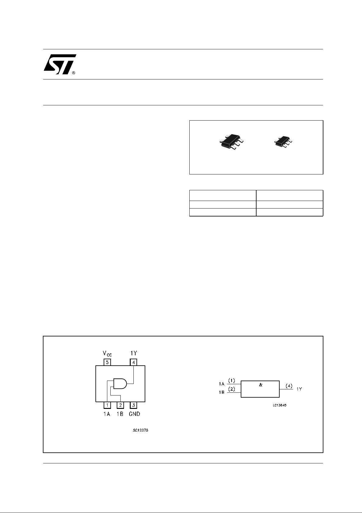
SOT323-5LSOT23-5L
ORDER CODES
PACKAGE T & R
SOT23-5L 74V1T08STR
SOT323-5L 74V1T08CTR
Power down protection is provided on all inputs
and 0 to 7V can be accepted on inp uts with no
regard to the supply voltage. This device can be
usedto interface 5V to 3V.
PIN CONNECTION AND IEC LOGIC SYMBOLS
1/9April 2004
74V1T08
INPUT EQUIVALENT CIRCUIT PIN DESCRIPTION
PIN N° SYMBOL NAME AND FUNCTION
1 1A Data Input
2 1B Data Input
4 1Y Data Output
3 GND Ground (0V)
5
TRUTH TABLE
ABY
LLL
LHL
HLL
HHH
ABSOLUTE MAXIMUM RATINGS
Symbol Parameter Value Unit
V
V
V
I
I
OK
I
I
or I
CC
T
T
Absolute Maximum Ratings are those values beyond which damage to the device may occur. Functional operation under these conditions is
not implied
Supply Voltage
CC
DC Input Voltage
I
DC Output Voltage -0.5 to VCC+0.5
O
DC Input Diode Current
IK
DC Output Diode Current
DC Output Current
O
DC VCCor Ground Current
GND
Storage Temperature
stg
Lead Temperature (10 sec)
L
V
CC
Positive Supply Voltage
-0.5 to +7.0 V
-0.5 to +7.0 V
-20 mA
± 20 mA
± 25 mA
± 50 mA
-65 to +150 °C
300 °C
V
RECOMMENDED OPERATING CONDITIONS
Symbol Parameter Value Unit
V
V
V
T
dt/dv
1) VINfrom0.8Vto 2V
2/9
Supply Voltage
CC
Input Voltage
I
Output Voltage 0 to V
O
Operating Temperature
op
Input Rise and Fall Time (note 1) (V
=5.0± 0.5V)
CC
4.5 to 5.5 V
0to5.5 V
CC
-55 to 125 °C
0 to 20 ns/V
V
DC SPECIFICATIONS
Symbol Parameter
V
V
V
+I
High Level Input
IH
Voltage
V
Low Level Input
IL
Voltage
High Level Output
OH
Voltage
Low Level Output
OL
Voltage
I
Input Leakage
I
Current
I
Quiescent Supply
CC
Current
Additional Worst
CC
Case Supply
Current
Test Condition Value
T
= 25°C
V
CC
(V)
4.5to
A
Min. Typ. Max. Min. Max. Min. Max.
222V
5.5
4.5to
5.5
4.5
4.5
4.5
4.5
0to
5.5
5.5
IO=-50 µA 4.4 4.5 4.4 4.4 V
=-8 mA 3.94 3.8 3.7
I
O
IO=50 µA 0.0 0.1 0.1 0.1 V
I
=8 mA 0.36 0.44 0.55
O
VI=5.5VorGND
V
I=VCC
or GND
One Input at 3.4V,
other input at V
5.5
CC
or GND
74V1T08
-40 to 85°C -55 to 125°C
0.8 0.8 0.8 V
± 0.1 ± 1.0 ± 1.0 µA
11020µA
1.35 1.5 1.5 mA
Unit
AC ELECTRICAL CHARACTERISTICS (Input t
r=tf
=3ns)
Test Condition Value
Symbol Parameter
t
t
(*) Voltage rangeis 5.0V ± 0.5V
Propagation Delay
PLH
Time
PHL
T
V
CC
(V)
C
(pF)
L
A
Min. Typ. Max. Min. Max. Min. Max.
5.0 (*) 15 3.9 6.7 1.0 7.5 1.0 8.5
5.0 (*) 50 4.5 7.7 1.0 8.5 1.0 9.5
-40 to 85°C -55 to 125°C
Unit
ns
= 25°C
CAPACITIVE CHARACTERISTICS
Test Condition Value
T
Symbol Parameter
C
C
Input Capacitance
IN
Power Dissipation
PD
Capacitance
(note 1)
1) CPDis defined as the value of the IC’s internal equivalent capacitance which is calculated from the operating current consumption without
load. (Refer to Test Circuit). Average operating current can be obtained by the following equation. I
= 25°C
A
-40 to 85°C -55 to 125°C
Min. Typ. Max. Min. Max. Min. Max.
410 10 10pF
14 pF
CC(opr)=CPDxVCCxfIN+ICC
Unit
3/9
 Loading...